ICGOO在线商城 > 集成电路(IC) > 接口 - 模拟开关,多路复用器,多路分解器 > NLAS1053USG
 Datasheet下载
- 型号: NLAS1053USG
- 制造商: ON Semiconductor
- 库位|库存: xxxx|xxxx
- 要求:
| 数量阶梯 | 香港交货 | 国内含税 |
| +xxxx | $xxxx | ¥xxxx |
查看当月历史价格
查看今年历史价格
NLAS1053USG产品简介:
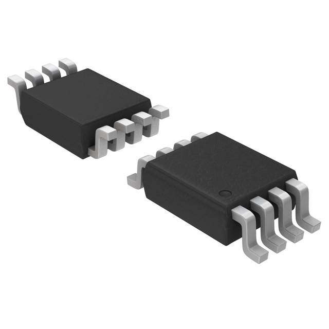
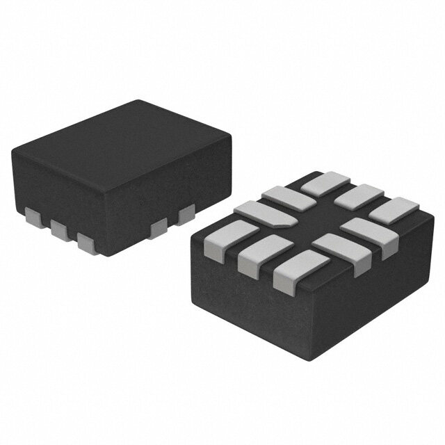
ICGOO电子元器件商城为您提供NLAS1053USG由ON Semiconductor设计生产,在icgoo商城现货销售,并且可以通过原厂、代理商等渠道进行代购。 NLAS1053USG价格参考¥2.23-¥5.44。ON SemiconductorNLAS1053USG封装/规格:接口 - 模拟开关,多路复用器,多路分解器, 1 Circuit IC Switch 2:1 16 Ohm US8。您可以下载NLAS1053USG参考资料、Datasheet数据手册功能说明书,资料中有NLAS1053USG 详细功能的应用电路图电压和使用方法及教程。
| 参数 | 数值 |
| 产品目录 | 集成电路 (IC)半导体 |
| 描述 | IC SWITCH SPDT US8多路器开关 IC 2:1 Mux/Demux Switch -55 to 125deg C |
| 产品分类 | |
| 品牌 | ON Semiconductor |
| 产品手册 | |
| 产品图片 |
|
| rohs | 符合RoHS无铅 / 符合限制有害物质指令(RoHS)规范要求 |
| 产品系列 | 开关 IC,多路器开关 IC,ON Semiconductor NLAS1053USG- |
| 数据手册 | |
| 产品型号 | NLAS1053USG |
| 产品目录页面 | |
| 产品种类 | 多路器开关 IC |
| 传播延迟时间 | 18 ns |
| 供应商器件封装 | US8 |
| 其它名称 | NLAS1053USGOSCT |
| 功能 | |
| 包装 | 剪切带 (CT) |
| 商标 | ON Semiconductor |
| 安装类型 | 表面贴装 |
| 安装风格 | SMD/SMT |
| 导通电阻 | 22 欧姆 |
| 导通电阻—最大值 | 70 Ohms |
| 封装 | Reel |
| 封装/外壳 | 8-VFSOP(0.091",2.30mm 宽) |
| 封装/箱体 | US8-8 |
| 工作温度 | -55°C ~ 125°C |
| 工作电源电压 | 2 V to 5.5 V |
| 工厂包装数量 | 3000 |
| 带宽 | 170 MHz |
| 开关数量 | 1 |
| 最大功率耗散 | 250 mW |
| 最大工作温度 | + 125 C |
| 最小工作温度 | - 55 C |
| 标准包装 | 1 |
| 电压-电源,单/双 (±) | 2 V ~ 5.5 V |
| 电压源 | 单电源 |
| 电流-电源 | 1µA |
| 电路 | 1 x SPDT |
| 空闲时间—最大值 | 12 ns |
| 系列 | NLAS1053 |
| 运行时间—最大值 | 12 ns |
| 通道数量 | 1 Channel |


- 商务部:美国ITC正式对集成电路等产品启动337调查
- 曝三星4nm工艺存在良率问题 高通将骁龙8 Gen1或转产台积电
- 太阳诱电将投资9.5亿元在常州建新厂生产MLCC 预计2023年完工
- 英特尔发布欧洲新工厂建设计划 深化IDM 2.0 战略
- 台积电先进制程称霸业界 有大客户加持明年业绩稳了
- 达到5530亿美元!SIA预计今年全球半导体销售额将创下新高
- 英特尔拟将自动驾驶子公司Mobileye上市 估值或超500亿美元
- 三星加码芯片和SET,合并消费电子和移动部门,撤换高东真等 CEO
- 三星电子宣布重大人事变动 还合并消费电子和移动部门
- 海关总署:前11个月进口集成电路产品价值2.52万亿元 增长14.8%


PDF Datasheet 数据手册内容提取
NLAS1053 2:1 Mux/Demux Analog Switches The NLAS1053 is an advanced CMOS analog switch fabricated with silicon gate CMOS technology. It achieves very high speed propagation delays and low ON resistances while maintaining CMOS low power dissipation. The device consists of a single 2:1 www.onsemi.com Mux/Demux (SPDT), similar to ON Semiconductor’s NLAS4053 MARKING analog and digital voltages that may vary across the full power supply DIAGRAM range (from V to GND). CC The inhibit and select input pins have over voltage protection that 8 allows voltages above V up to 7.0 V to be present without damage CC or disruption of operation of the part, regardless of the operating US8 8 AC M(cid:2) voltage. US SUFFIX (cid:2) CASE 493 1 Features • High Speed: tPD = 1 ns (Typ) at VCC = 5.0 V 1 • Low Power Dissipation: ICC = 2 (cid:2)A (Max) at TA = 25°C AC = Specific Device Code • High Bandwidth, Improved Linearity, and Low RDS M = Date Code • ON (cid:2) = Pb−Free Package INH Pin Allows a Both Channels ‘OFF’ Condition (With a High) (Note: Microdot may be in either location) • RDS ≅ 25 (cid:3), Performance Very Similar to the NLAS4053 ON • Break Before Make Circuitry, Prevents Inadvertent Shorts • Useful For Switching Video Frequencies Beyond 50 MHz FUNCTION TABLE • Latchup Performance Exceeds 300 mA INH Select Ch 0 Ch 1 • ESD Performance: HBM > 2000 V; MM > 200 V, CDM > 1500 V • H X OFF OFF Tiny US8 Package, Only 2.1 X 3.0 mm • L L ON OFF These Devices are Pb−Free, Halogen Free/BFR Free and are RoHS L H OFF ON Compliant COM 1 8 VCC ORDERING INFORMATION INH 2 7 CH0 Device Package Shipping† NLAS1053USG US8 3000 / Tape & Reel N/C 3 6 CH1 (Pb−Free) †For information on tape and reel specifications, GND 4 5 Select including part orientation and tape sizes, please refer to our Tape and Reel Packaging Specifications Brochure, BRD8011/D. Figure 1. Pin Assignment © Semiconductor Components Industries, LLC, 2015 1 Publication Order Number: July, 2015 − Rev. 3 NLAS1053/D
NLAS1053 MAXIMUM RATINGS Parameter Symbol Value Unit Positive DC Supply Voltage VCC −0.5 to +7.0 V Digital Input Voltage (Select and Inhibit) VIN −0.5 ≤ V is ≤ +7.0 V Analog Output Voltage (VCH or VCOM) VIS −0.5 ≤ V is ≤ VCC +0.5 V DC Current, Into or Out of Any Pin IIK 50 mA Storage Temperature Range TSTG −65 to +150 (cid:3)C Lead Temperature, 1 mm from Case for 10 Seconds TL 260 (cid:3)C Junction Temperature under Bias TJ +150 (cid:3)C Thermal Resistance (cid:4)JA 250 (cid:3)C/W Power Dissipation in Still Air at 85(cid:3)C PD 250 mW Moisture Sensitivity MSL Level 1 Flammability Rating Oxygen Index: 30% − 35% FR UL 94 V−0 @ 0.125 in ESD Withstand Voltage Human Body Model (Note 2) VESD > 2000 V Machine Model (Note 3) 200 Charged Device Model (Note 4) N/A Latchup Performance Above VCC and Below GND at 85(cid:3)C (Note 5) ILatchup ±300 mA Stresses exceeding those listed in the Maximum Ratings table may damage the device. If any of these limits are exceeded, device functionality should not be assumed, damage may occur and reliability may be affected. 1. Measured with minimum pad spacing on an FR4 board, using 10 mm−by−1 inch, 2−ounce copper trace with no air flow. 2. Tested to EIA/JESD22−A114−A. 3. Tested to EIA/JESD22−A115−A. 4. Tested to JESD22−C101−A. 5. Tested to EIA/JESD78. RECOMMENDED OPERATING CONDITIONS Characteristics Symbol Min Max Unit Positive DC Supply Voltage VCC 2.0 5.5 V Digital Input Voltage (Select and Inhibit) VIN GND 5.5 V Static or Dynamic Voltage Across an Off Switch VIO GND VCC V Analog Input Voltage (CH, COM) VIS GND VCC V Operating Temperature Range, All Package Types TA −55 +125 °C Input Rise or Fall Time Vcc = 3.3 V ± 0.3 V tr, tf 0 100 ns/V (Enable Input) Vcc = 5.0 V ± 0.5 V 0 20 Functional operation above the stresses listed in the Recommended Operating Ranges is not implied. Extended exposure to stresses beyond the Recommended Operating Ranges limits may affect device reliability. DEVICE JUNCTION TEMPERATURE VERSUS TIME E TO 0.1% BOND FAILURES T A FAILURE RATE OF PLASTIC = CERAMIC R Junction E UNTIL INTERMETALLICS OCCUR Tempe89ra00ture (cid:2)C Ti1m4,01e39, 2,H3,20o00u0rs Tim1e41,77 Y..98ears ED FAILUR °T = 130CJ °T = 120CJ °T = 110CJ ° = 100CTJ °T = 90CJ °T = 80CJ Z 100 178,700 20.4 ALI 1 M 110 79,600 9.4 R O N 1 10 100 1000 120 37,000 4.2 TIME, YEARS 130 17,800 2.0 Figure 2. Failure Rate versus 140 8,900 1.0 Time Junction Temperature www.onsemi.com 2
NLAS1053 DC CHARACTERISTICS − Digital Section (Voltages Referenced to GND) Guaranteed Limit Parameter Condition Symbol VCC (cid:2)55(cid:2)C to 25(cid:2)C (cid:3)85(cid:2)C (cid:3)125(cid:2)C Unit Minimum High−Level Input VIH 2.0 1.5 1.5 1.5 V Voltage, Select and Inhibit 2.5 1.9 1.9 1.9 Inputs 3.0 2.1 2.1 2.1 4.5 3.15 3.15 3.15 5.5 3.85 3.85 3.85 Maximum Low−Level Input VIL 2.0 0.5 0.5 0.5 V Voltage, Select and Inhibit 2.5 0.6 0.6 0.6 Inputs 3.0 0.9 0.9 0.9 4.5 1.35 1.35 1.35 5.5 1.65 1.65 1.65 Maximum Input Leakage VIN = 5.5 V or GND IIN 0 V to 5.5 V (cid:2)0.1 (cid:2)1.0 (cid:2)1.0 (cid:2)A Current, Select and Inhibit Inputs Maximum Quiescent Supply Select and Inhibit = VCC or GND ICC 5.5 1.0 1.0 2.0 (cid:2)A Current DC ELECTRICAL CHARACTERISTICS − Analog Section Guaranteed Limit Parameter Condition Symbol VCC (cid:2)55 to 25(cid:2)C (cid:3) 85(cid:2)C (cid:3) 125(cid:2)C Unit Maximum “ON” VIN = VIL or VIH RON 2.5 70 85 105 (cid:3) Resistance VIS = GND to VCC 3.0 40 46 52 (Figures 17 − 23) IINI ≤ 10.0 mA 4.5 20 28 34 5.5 16 22 28 ON Resistance Flatness VIN = VIL or VIH RFLAT 4.5 4 4 5 (cid:3) (Figures 17 − 23) IINI ≤ 10.0 mA (ON) VIS = 1V, 2V, 3.5V ON Resistance Match VIN = VIL or VIH (cid:5)RON 4.5 2 2 3 (cid:3) Between Channels IINI ≤ 10.0 mA (ON) VCH1 or VCH0 = 3.5 V CH1 or CH0 Off Leakage VIN = VIL or VIH ICH0 5.5 1 10 100 nA Current (Figure 9) VCH1 or VCH0 = 1.0 VCOM 4.5 V ICH1 COM ON Leakage VIN = VIL or VIH ICOM(ON) 5.5 1 10 100 nA Current (Figure 9) VCH1 1.0 V or 4.5 V with VCH0 floating or VCH1 1.0 V or 4.5 V with VCH1 floating VCOM = 1.0 V or 4.5 V www.onsemi.com 3
NLAS1053 AC ELECTRICAL CHARACTERISTICS (Input tr = tf = 3.0 ns) Guaranteed Max Limit (cid:2)55 to 25(cid:2)C (cid:3) 85(cid:2)C (cid:3) 125(cid:2)C VCC Parameter Test Conditions Symbol (V) Min Typ* Max Min Max Min Max Unit Turn−On Time RL = 300 (cid:3)(cid:6) CL = 35 pF tON 2.5 2 7 12 2 15 2 15 ns (Figures 12 and 13) (Figures 4 and 5) 3.0 2 5 10 2 15 2 15 INH to Output 4.5 1 4 9 1 12 1 12 5.5 1 3 8 1 12 1 12 Turn−Off Time RL = 300 (cid:3)(cid:6) CL = 35 pF tOFF 2.5 2 7 12 2 15 2 15 ns (Figures 12 and 13) (Figures 4 and 5) 3.0 2 5 10 2 15 2 15 INH to Output 4.5 1 4 9 1 12 1 12 5.5 1 3 8 1 12 1 12 Transition Time (Channel Selec- RL = 300 (cid:3)(cid:6) CL = 35 pF ttrans 2.5 5 18 28 5 30 5 30 ns tion Time) (Figures and ) 3.0 5 13 21 5 25 5 25 (Figure ) 4.5 2 12 16 2 20 2 20 Select to Output 5.5 2 9 14 2 20 2 20 Minimum VIS = 3.0 V (Figure 3) tBBM 2.5 1 12 1 1 ns Break−Before−Make Time RL = 300 (cid:3)(cid:6) CL = 35 pF 3.0 1 11 1 1 4.5 1 6 1 1 5.5 1 5 1 1 Typical @ 25, VCC = 5.0 V Maximum Input Capacitance, Select/INH Input CIN 8 pF Analog I/O (switch off) CNO or CNC 10 Common I/O (switch off) CCOM 10 Feedthrough (switch on) C(ON) 20 *Typical Characteristics are at 25(cid:3)C. ADDITIONAL APPLICATION CHARACTERISTICS (Voltages Referenced to GND Unless Noted) ÎÎÎÎ Typical ÎÎÎÎVCC Parameter Condition Symbol V 25°C Unit ÎÎÎÎÎÎÎÎ Maximum On−Channel −3dB Bandwidth or VIN = 0 dBm ÎÎBÎW Î 3.0 170 MHz Minimum Frequency Response VIN centered between VCC and GND 4.5 200 (Figure 10) (Figure 7) ÎÎÎÎÎÎÎÎ 5.5 200 Maximum Feedthrough On Loss VIN = 0 dBm @ 100 kHz to 50 MHz ÎÎVOÎNL Î 3.0 −3 dB V(FINig cueren t7e)red between VCC and GND ÎÎÎÎ 45..55 −−33 Off−Channel Isolation f = 100 kHz; VIS = 1 V RMS ÎÎÎÎVIÎÎSO ÎÎ 3.0 −93 dB (Figure 10) VIN centered between VCC and GND ÎÎÎÎ 4.5 −93 (Figure 7) 5.5 −93 ÎÎÎÎÎÎÎÎ Charge Injection Select Input to VIN = VCC to GND, FIS = 20 kHz Q Common I/O tr = tf = 3 ns ÎÎÎÎ 3.0 1.5 pC (Figure 15) RQI S= =C 0L *(cid:3) (cid:5), VCOL U=T 1000 pF ÎÎÎÎ 5.5 3.0 (Figure 8) ÎÎÎÎÎÎÎÎ Total Harmonic Distortion FIS = 20 Hz to 100 kHz, RL = Rgen = 600 (cid:3) ÎÎTHÎD Î THD + Noise CL = 50 pF (Figure 14) VIS = 5.0 VPP sine wave ÎÎÎÎ 5.5 0.1 % www.onsemi.com 4
NLAS1053 DUT VCC VCC Output Input 0.1 (cid:2)F VOUT GND 300 35 pF tBMM (cid:3) 90% 90% of VOH Output Switch Select Pin GND Figure 3. t (Time Break−Before−Make) BBM VCC DUT Input 50% 50% VCC Output 0 V 0.1 (cid:2)F VOUT Open VOH 300 35 pF 90% 90% (cid:3) Output INH VOL Input tON tOFF Figure 4. t /t ON OFF VCC VCC DUT Input 50% 50% 300 (cid:3) 0 V Output VOUT VOH Open 35 pF Output 10% 10% INH VOL Input tOFF tON Figure 5. t /t ON OFF www.onsemi.com 5
NLAS1053 VCC Output VCC Input 50% 50% 0.1 (cid:2)F VOUT GND 0 V 300 35 pF (cid:3) VCC 90% Output Select Pin 10% GND ttrans ttrans Figure 6. t (Channel Selection Time) trans 50 (cid:3) DUT Reference Input Transmitted Output 50 (cid:3) Generator 50 (cid:3) Channel switch control/s test socket is normalized. Off isolation is measured across an off channel. On loss is the bandwidth of an On switch. VISO, Bandwidth and VONL are independent of the input signal direction. (cid:3) (cid:4) VOUT VISO = Off Channel Isolation = 20 Log V I N for VIN at 100 kHz (cid:3) (cid:4) VOUT VONL = On Channel Loss = 20 Log V I N for VIN at 100 kHz to 50 MHz Bandwidth (BW) = the frequency 3 dB below VONL Figure 7. Off Channel Isolation/On Channel Loss (BW)/Crosstalk (On Channel to Off Channel)/V ONL DUT VCC Open Output VIN GND CL Output Off On Off (cid:5)VOUT VIN Figure 8. Charge Injection: (Q) www.onsemi.com 6
NLAS1053 100 0 Bandwidth (ON−RESPONSE) 10 −20 A) n 1 −40 GE ( B) Off Isolation AKA 0.1 ICOM(ON) (d −60 E L ICOM(OFF) 0.01 VCC = 5.0 V −80 VTAC C= =2 55(cid:3).0C V ICH(OFF) 0.001 −100 −55 −20 25 70 85 125 0.01 0.1 1 10 100 200 TEMPERATURE (°C) FREQUENCY (MHz) Figure 9. Switch Leakage versus Temperature Figure 10. Bandwidth and Off−Channel Isolation 30 0 25 10 e) 20 E (Degre 20 ME (ns) 15 AS TI ttrans (ns) H 10 P 30 VTAC C= =2 55(cid:3).0C V 5 tON/tOFF (ns) 0 0.01 0.1 1 10 100 200 2.5 3 3.5 4 4.5 5 FREQUENCY (MHz) VCC (VOLTS) Figure 11. Phase versus Frequency Figure 12. t and t versus V at 25(cid:2)C ON OFF CC 30 1 VCC = 4.5 V VINpp = 3.0 V 25 VCC = 3.6 V 20 %) ns) SE ( E ( 15 NOI 0.1 TIM 10 ttrans HD + VVICNCp p= = 5 5.5.0 V V T 5 tON/tOFF 0 0.01 −55 −40 25 85 125 1 10 100 Temperature (°C) FREQUENCY (kHz) Figure 13. t and t versus Temp Figure 14. Total Harmonic Distortion ON OFF Plus Noise versus Frequency www.onsemi.com 7
NLAS1053 3.0 100 2.5 10 2.0 VCC = 5 V 1 1.5 0.1 C) A) Q (p 1.0 (nCC 0.01 I VCC = 3.0 V 0.5 VCC = 3 V 0.001 0 0.0001 VCC = 5.0 V −0.5 0.00001 0 1 2 3 4 5 −40 −20 0 20 60 80 100 120 VCOM (V) Temperature (°C) Figure 16. I versus Temp, V = 3 V & 5 V Figure 15. Charge Injection versus COM Voltage CC CC 100 100 90 VCC = 2.0 V 80 80 70 (cid:3)) 60 (cid:3)) 60 N ( N ( 50 85°C RO 40 VCC = 2.5 V RO 40 VCC = 3.0 V 30 125°C 20 VCC = 4.5 V 20 25°C −55°C 10 0 0 0 1 2 3 4 5 0 0.5 1 1.5 2 2.5 VCOM (VOLTS) VCOM (VOLTS) Figure 17. RON versus VCOM and VCC (@ 25(cid:2)C Figure 18. RON versus VCOM and Temperature, VCC 2.0 V 70 40 60 25°C 35 30 50 25 25°C (cid:3)) 40 (cid:3)) N ( N ( 20 125°C O O 30 R R 125°C 15 85°C 20 10 −55°C 85°C 10 −55°C 5 0 0 0 0.5 1 1.5 2 2.5 3 0 0.5 1 1.5 2 2.5 3 3.5 VCOM (VOLTS) VCOM (VOLTS) Figure 19. RON versus VCOM and Temperature, Figure 20. RON versus VCOM and Temperature, V = 2.5 V V = 3.0 V CC CC www.onsemi.com 8
NLAS1053 20 18 18 16 16 125°C 14 125°C 14 12 12 85°C (cid:3)) (cid:3)) 10 N ( 10 N ( 85°C O O 8 R 8 R −55°C 6 6 25°C −55°C 25°C 4 4 2 2 0 0 0 1 2 3 4 5 0 1 2 3 4 5 6 VCOM (VOLTS) VCOM (VOLTS) Figure 21. RON versus VCOM and Temperature, Figure 22. RON versus VCOM and Temperature, VCC = 4.5 V VCC = 5.0 V 20 15 125°C (cid:3)) N ( 10 85°C O R 25°C 5 −55°C 0 0 1 2 3 4 5 6 VCOM (VOLTS) Figure 23. R versus V and Temperature, ON COM V = 5.5 V CC www.onsemi.com 9
NLAS1053 PACKAGE DIMENSIONS US8 US SUFFIX CASE 493−02 ISSUE D NOTES: X Y 1. DIMENSIONING AND TOLERANCING PER ANSI A J Y14.5M, 1982. 8 5 2. CONTROLLING DIMENSION: MILLIMETERS. 3. DIMENSION A DOES NOT INCLUDE MOLD FLASH, PROTRUSION OR GATE BURR. MOLD FLASH. PROTRUSION AND GATE BURR SHALL NOT EXCEED 0.14MM (0.0055”) PER SIDE. DETAIL E 4. DIMENSION B DOES NOT INCLUDE INTERLEAD FLASH OR PROTRUSION. INTERLEAD FLASH B L AND PROTRUSION SHALL NOT EXCEED 0.14MM (0.0055”) PER SIDE. 5. LEAD FINISH IS SOLDER PLATING WITH THICKNESS OF 0.0076−0.0203MM (0.003−0.008”). 6. ALL TOLERANCE UNLESS OTHERWISE SPECIFIED ±0.0508MM (0.0002”). 1 4 R MILLIMETERS INCHES G S DIM MIN MAX MIN MAX P A 1.90 2.10 0.075 0.083 U B 2.20 2.40 0.087 0.094 C 0.60 0.90 0.024 0.035 C D 0.17 0.25 0.007 0.010 H F 0.20 0.35 0.008 0.014 SPELAATNIENG D K 0.10 (0.004) T N GH 00..5400 BRSECF 00..002106 BRSECF J 0.10 0.18 0.004 0.007 T R 0.10 TYP 0.10 (0.004) M T X Y K 0.00 0.10 0.000 0.004 L 3.00 3.20 0.118 0.128 M 0 (cid:3) 6 (cid:3) 0 (cid:3) 6 (cid:3) V N 0 (cid:3) 10 (cid:3) 0 (cid:3) 10 (cid:3) M P 0.23 0.34 0.010 0.013 R 0.23 0.33 0.009 0.013 S 0.37 0.47 0.015 0.019 U 0.60 0.80 0.024 0.031 F V 0.12 BSC 0.005 BSC DETAIL E RECOMMENDED SOLDERING FOOTPRINT* 8X 0.30 8X 0.68 3.40 1 0.50 PITCH DIMENSIONS: MILLIMETERS *For additional information on our Pb−Free strategy and soldering details, please download the ON Semiconductor Soldering and Mounting Techniques Reference Manual, SOLDERRM/D. ON Semiconductor and the are registered trademarks of Semiconductor Components Industries, LLC (SCILLC) or its subsidiaries in the United States and/or other countries. SCILLC owns the rights to a number of patents, trademarks, copyrights, trade secrets, and other intellectual property. A listing of SCILLC’s product/patent coverage may be accessed at www.onsemi.com/site/pdf/Patent−Marking.pdf. SCILLC reserves the right to make changes without further notice to any products herein. SCILLC makes no warranty, representation or guarantee regarding the suitability of its products for any particular purpose, nor does SCILLC assume any liability arising out of the application or use of any product or circuit, and specifically disclaims any and all liability, including without limitation special, consequential or incidental damages. “Typical” parameters which may be provided in SCILLC data sheets and/or specifications can and do vary in different applications and actual performance may vary over time. All operating parameters, including “Typicals” must be validated for each customer application by customer’s technical experts. SCILLC does not convey any license under its patent rights nor the rights of others. SCILLC products are not designed, intended, or authorized for use as components in systems intended for surgical implant into the body, or other applications intended to support or sustain life, or for any other application in which the failure of the SCILLC product could create a situation where personal injury or death may occur. Should Buyer purchase or use SCILLC products for any such unintended or unauthorized application, Buyer shall indemnify and hold SCILLC and its officers, employees, subsidiaries, affiliates, and distributors harmless against all claims, costs, damages, and expenses, and reasonable attorney fees arising out of, directly or indirectly, any claim of personal injury or death associated with such unintended or unauthorized use, even if such claim alleges that SCILLC was negligent regarding the design or manufacture of the part. SCILLC is an Equal Opportunity/Affirmative Action Employer. This literature is subject to all applicable copyright laws and is not for resale in any manner. PUBLICATION ORDERING INFORMATION LITERATURE FULFILLMENT: N. American Technical Support: 800−282−9855 Toll Free ON Semiconductor Website: www.onsemi.com Literature Distribution Center for ON Semiconductor USA/Canada P.O. Box 5163, Denver, Colorado 80217 USA Europe, Middle East and Africa Technical Support: Order Literature: http://www.onsemi.com/orderlit Phone: 303−675−2175 or 800−344−3860 Toll Free USA/Canada Phone: 421 33 790 2910 Fax: 303−675−2176 or 800−344−3867 Toll Free USA/Canada Japan Customer Focus Center For additional information, please contact your local Email: orderlit@onsemi.com Phone: 81−3−5817−1050 Sales Representative www.onsemi.com NLAS1053/D 10
Mouser Electronics Authorized Distributor Click to View Pricing, Inventory, Delivery & Lifecycle Information: O N Semiconductor: NLAS1053USG