ICGOO在线商城 > 集成电路(IC) > 线性 - 音頻放大器 > NJU8752V-TE1
- 型号: NJU8752V-TE1
- 制造商: NJR
- 库位|库存: xxxx|xxxx
- 要求:
| 数量阶梯 | 香港交货 | 国内含税 |
| +xxxx | $xxxx | ¥xxxx |
查看当月历史价格
查看今年历史价格
NJU8752V-TE1产品简介:
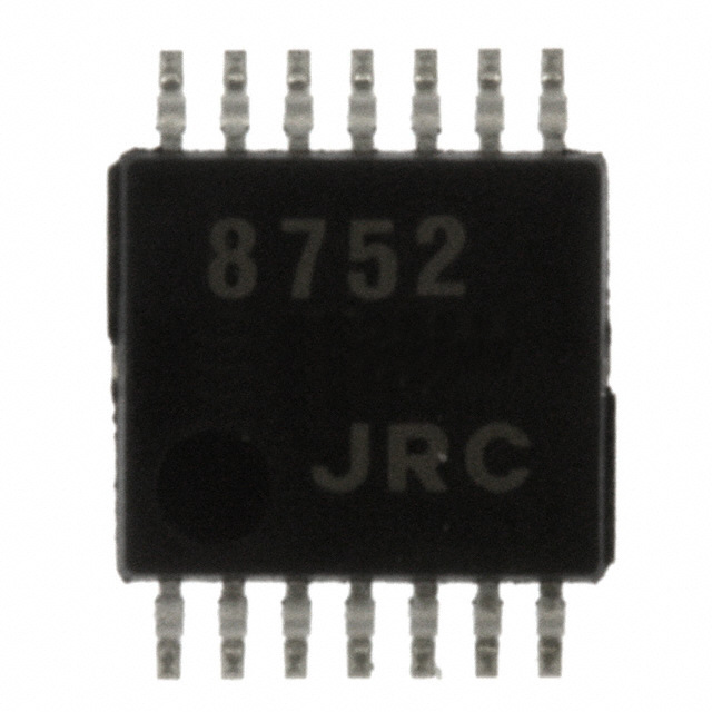
ICGOO电子元器件商城为您提供NJU8752V-TE1由NJR设计生产,在icgoo商城现货销售,并且可以通过原厂、代理商等渠道进行代购。 NJU8752V-TE1价格参考。NJRNJU8752V-TE1封装/规格:线性 - 音頻放大器, Amplifier IC 1-Channel (Mono) Class D 14-SSOP。您可以下载NJU8752V-TE1参考资料、Datasheet数据手册功能说明书,资料中有NJU8752V-TE1 详细功能的应用电路图电压和使用方法及教程。
| 参数 | 数值 |
| 产品目录 | 集成电路 (IC) |
| 描述 | IC AMP D FOR PIEZO SPKR 14-SSOP |
| 产品分类 | |
| 品牌 | NJR |
| 数据手册 | |
| 产品图片 | |
| 产品型号 | NJU8752V-TE1 |
| rohs | 无铅 / 符合限制有害物质指令(RoHS)规范要求 |
| 产品系列 | - |
| 不同负载时的最大输出功率x通道数 | - |
| 产品目录页面 | |
| 供应商器件封装 | 14-SSOP |
| 其它名称 | NJU#8752V-TE1CT |
| 包装 | 剪切带 (CT) |
| 安装类型 | 表面贴装 |
| 封装/外壳 | 14-LSSOP(0.173",4.40mm 宽) |
| 工作温度 | -40°C ~ 85°C (TA) |
| 标准包装 | 1 |
| 特性 | 静音,短路保护,待机 |
| 电压-电源 | 2.7 V ~ 3.6 V |
| 类型 | D 类 |
| 输出类型 | 1-通道(单声道) |





- 商务部:美国ITC正式对集成电路等产品启动337调查
- 曝三星4nm工艺存在良率问题 高通将骁龙8 Gen1或转产台积电
- 太阳诱电将投资9.5亿元在常州建新厂生产MLCC 预计2023年完工
- 英特尔发布欧洲新工厂建设计划 深化IDM 2.0 战略
- 台积电先进制程称霸业界 有大客户加持明年业绩稳了
- 达到5530亿美元!SIA预计今年全球半导体销售额将创下新高
- 英特尔拟将自动驾驶子公司Mobileye上市 估值或超500亿美元
- 三星加码芯片和SET,合并消费电子和移动部门,撤换高东真等 CEO
- 三星电子宣布重大人事变动 还合并消费电子和移动部门
- 海关总署:前11个月进口集成电路产品价值2.52万亿元 增长14.8%



PDF Datasheet 数据手册内容提取
NJU8N7J5U23/5525B5 PRELIMINARY Analog Signal Input Class D Amplifier for Piezo Speaker ! GENERAL DESCRIPTION ! PACKAGE OUTLINE The NJU8752/NJU8752B is an analog signal input monaural class D amplifier for Piezo speaker. The NJU8752/52B includes Inversion operational amplifier input circuit, PWM modulator, an output-short protector and a low voltage detector. Input part operates on 3.3V(TYP) as power supply and Output part operates up to 16.0V(MAX). Therefore, it drives Piezo speaker NJU8752V / 52BV with louder sound and High efficiency. The NJU8752/52B incorporates BTL amplifier, which eliminate AC coupling capacitors, capable of driving Piezo speaker with simple external LC low-pass filters. Class D operation achieves lower power operation for NJU8752BKM1 Piezo speaker, thus the NJU8752/52B is suited for battery powered applications. ! FEATURES NJU8752BKP4 # Piezo Speaker Driving # 1-channel Analog Signal Input, 1-channel BTL Output # Standby(Hi-Z), Mute Control # Voltage Gain 31dB(NJU8752) 20dB(NJU8752B) # Built-in Low Voltage Detector # Built-in Short Protector # Operating Voltage Input: 2.7 ~ 3.6V (NJU8752) 3.1 ~ 3.6V (NJU8752B) Output: 6.0 ~ 16.0V # C-MOS Technology # Package Outline SSOP14 (NJU8752 / 52B) QFN20 / QFN28 (NJU8752B) ! PIN CONFIGURATION V 1 14 V DD SS IN 2 13 COM TEST 1 3 12 TEST 2 MUTVEB 45 1110 SVTB YB 28 NC NC V DDNC V SSNC NC SS SS OUT 6 9 OUT 1 P N V 7 8 V IN COM DDO DDO TEST 1 NC SSOP14 (NJU8752V / 52BV) MUTEB TEST 2 NC STBYB V V 20 NC V DDNC V SSNC NSCS NCSS 1 OUT OUT P N IN COM TEST 1 TEST 2 DO DOCCCDO DO MUTEB STBYB VDVDNNNVDVD VSS VSS QFN28 (NJU8752BKP4) OUT OUT P N O OC O O DD DDN DD DD VV VV QFN20 (NJU8752BKM1) Ver.2004-08-05 -1-
NJU8752/52B ! BLOCK DIAGRAM VDD VSS V DDO IN - OUT P + Pulse VSS Width Modulator - VDDO COM + OUT N V SS Short Protector Soft Start Control Logic Low Voltage Detector MUTEB TEST 1 STBYB TEST 2 ! PIN DESCRIPTION No. SYMBOL I/O Function SSOP14 QFN20 QFN28 1 19 26 V − Power Supply: V =3.3V DD DD 2 1 1 IN I Signal Input Maker test 1 3 2 2 TEST 1 I This pin must be connected to GND. Mute Control 4 3 3 MUTEB I Low : Mute ON High : Mute OFF 5,10,14 4,12,17 5,17,24 V − Power GND: V =0V SS SS 6 5 7 OUT O Positive Output P 7,8 6,7,9,10 8,9,13,14 V − Output Power Supply : V =16.0V max. DDO DDO 9 11 15 OUT O Negative Output N Standby Control 11 13 18 STBYB I Low : Standby ON High : Standby OFF Maker test 2 12 14 19 TEST 2 I This pin must be connected to GND. 13 15 21 COM − Analog common 4,6,10,11, − 8,16,18,20 12,16,20,22, NC − Non connection 23,25,27,28 *V (SSOP14:Pin No.5,10,14, QFN20:Pin No.4,12,17, QFN28:Pin No.5,17,24) should be connected SS at a nearest point to the IC. *V (SSOP14:Pin No.7,8, QFN20:Pin No.6,7,9,10, QFN28:Pin No.8,9,13,14) should be connected DDO at a nearest point to the IC. *MUTEB(SSOP14: Pin No.4, QFN20, QFN28:Pin No.3) and STBYB(SSOP14:Pin No.11, QFN20:Pin No.13, QFN28:Pin No.18) must be connected to V , when these pins are not used. DD - 2 - Ver.2004-08-05
NJU8N7J5U23/5525B5 ! FUNCTIONAL DESCRIPTION (1) Signal Output The OUT and OUT generate PWM output signals, which will be converted to analog signal via external P N 2nd-order or higher LC filter. A switching regulator with a high response against a voltage fluctuation is the best selection for the V , which are the power supply for output drivers. To obtain better THD performance, the DDO stabilization of the power is required. (2) Standby By setting the STBYB pin to (cid:147)L(cid:148), the standby mode is enabled. In the standby mode, the entire functions of the NJU8752/52B enter a low-power state, and the output pins (OUT and OUT ) are high impedance. P N (3) Mute By setting the MUTEB pin to (cid:147)L(cid:148), the Mute function is enabled. In the Mute mode, the output pins (OUT and P OUT ) output square wave (Duty: 50%). N (4) Low Voltage Detector When the power supply voltage drops down to below V (MIN), the internal oscillation is halted for prevention DD to generate unwanted frequency, and the output pins (OUT and OUT ) become in high impedance. P N (5) Short Circuit Protection The short protector, which protects the NJU8752/52B against high short-circuit current, turns off the output driver. After about 5 seconds from the protection, the NJU8752/52B returns to normal operation. The short protector functions at the following accidents. • Short between OUTP and OUTN • Short between OUTP and VSS • Short between OUTN and VSS Note 1) The detectable current and the period for the protection depend on the power supply voltage and ambient temperature. Note 2) The short protector is not effective for a long term short-circuit but for an instantaneous accident. Continuous high-current may cause permanent damage to the NJU8752/52B. Ver.2004-08-05 -3-
NJU8752/52B ! ABSOLUTE MAXIMUM RATINGS (Ta=25°C) PARAMETER SYMBOL RATING UNIT V -0.3 ~ +4.0 V Supply Voltage DD V -0.3 ~ +18.0 V DDO Input Voltage Vin -0.3 ~ V +0.3 V DD Operating Temperature Topr -40 ~ +85 °C Storage Temperature Tstg -40 ~ +125 °C SSOP14 450 Power Dissipation QFN20 P 620 mW D QFN28 640 * : Mounted on two-layer board of based on the JEDEC. Note 1) All voltage are relative to (cid:147)V =0V(cid:148) reference. SS Note 2) The LSI must be used inside of the (cid:147)Absolute maximum ratings(cid:148). Otherwise, a stress may cause permanent damage to the LSI. Note 3) De-coupling capacitors for V -V and V -V should be connected for stable operation. DD SS DDO SS ! ELECTRICAL CHARACTERISTICS -NJU8752- (Ta=25°C, V =3.3V, V =12.0V, V =0V,Input Signal=1kHz, Input Signal Level=200mVrms, DD DDO SS Frequency Band=20Hz~20kHz, Load Impedance=0.8µF, 2nd-order 34kHz LC Filter(Q=0.75)) PARAMETER SYMBOL CONDITIONS MIN TYP MAX UNIT Note V Supply Voltage V 2.7 3.3 3.6 V DD DD V Supply Voltage V 6.0 12.0 16.0 V DDO DDO Input Impedance Z IN pin - 20 - kΩ IN Voltage Gain A - 31 - dB V Input Signal Level Output THD THD - 0.05 0.08 % 4 =200mVrms Maximum Output Vo Output THD=10% 7 10 - Vrms S/N SN A weight - 80 - dB 4 Dynamic Range Drange A weight - 83 - dB 4 Maximum Mute Attenuation MAT 90 - - dB Operating Current(Stanby) I - - 1 µA ST Operating Current No-load operating I - 3.5 10 mA (No signal input) DD No Signal Input V MUTEB, STBYB pins 0.7V - V V Input Voltage IH DD DD V MUTEB, STBYB pins 0 - 0.3V V IL DD Input Leakage Current I MUTEB, STBYB pins - - –1.0 µA LK - 4 - Ver.2004-08-05
NJU8N7J5U23/5525B5 -NJU8752B- (Ta=25°C, V =3.3V, V =12.0V, V =0V,Input Signal=1kHz, Input Signal Level=700mVrms, DD DDO SS Frequency Band=20Hz~20kHz, Load Impedance=0.8µF, 2nd-order 34kHz LC Filter(Q=0.75)) PARAMETER SYMBOL CONDITIONS MIN TYP MAX UNIT Note V Supply Voltage V 3.1 3.3 3.6 V DD DD V Supply Voltage V 6.0 12.0 16.0 V DDO DDO Input Impedance Z IN pin - 20 - kΩ IN Voltage Gain A - 20 - dB V Input Signal Level Output THD THD - 0.05 0.08 % 4 =700mVrms Maximum Output Vo Output THD=10% 7 10 - Vrms S/N SN A weight - 80 - dB 4 Dynamic Range Drange A weight - 83 - dB 4 Maximum Mute Attenuation MAT - 90 - dB Operating Current(Stanby) I - - 1 µA ST Operating Current No-load operating I - 3.5 10 mA (No signal input) DD No Signal Input V MUTEB, STBYB pins 0.7V - V V Input Voltage IH DD DD V MUTEB, STBYB pins 0 - 0.3V V IL DD Input Leakage Current I MUTEB, STBYB pins - - –1.0 µA LK Note 4) Test system of the output THD, S/N and Dynamic Range The output THD, S/N and dynamic range are tested in the system shown in Figure 1, where a 2nd-order LC LPF and another filter incorporated in an audio analyzer are used. 2nd-order Filter THD Input Signal NJU8752/52B LC LPF 20kHz Measuring Apparatus (AES17) NJU8752/52B Test Board Audio Analyzer Figure 1. Output THD, S/N and Dynamic Range Test System 2nd-order LPF : Refer to (cid:147)Typical Application Circuit(cid:148). Filters : 22Hz HPF + 20kHz LPF(AES17) (with the A-Weight filter for S/N and Dynamic-range tests) Ver.2004-08-05 -5-
NJU8752/52B ! TYPICAL APPLICATION CIRCUIT •LLB2520 is manufactured by TOKO, INC. For detail information, please refer its technical papers. LLB2520 10µF 0.1µF 5~10Ω 33~47µH Piezo Speaker OUT (6) VDD VDD(1) P 0.1µF LLB2520 0.5~2µF VSS(14) 5~10Ω 33~47µH 0.1µF 3.3kΩ 2.2µF B OUTN(9) 2 IN IN(2) 5 0.1µF 10µF 0.01µF COM(13) 2/ VDDO(7) VDDO 5 7 10µF MUTEB(4) 8 VSS(5) U J STBYB(11) N 0.1µF 10µF TEST1(3) VDDO(8) VDDO V (10) TEST2(12) SS Figure 2.1 Application Circuit example (SSOP14) LLB2520 10µF 0.1µF 5~10Ω 33~47µH Piezo Speaker OUT (5) V V (19) P DD DD 0.1µF 0.5~2µF LLB2520 VSS(17) B OUT (11) 5~10Ω 33~47µH 0.1µF 3.3kΩ 2.2µF 2 N IN IN(1) /5 0.1µF 10µF 0.01µF COM(15) 52 VDDO(6,7) VDDO 7 8 10µF MUTEB(3) U VSS(4) J N STBYB(13) 0.1µF 10µF V (9,10) V TEST1(2) DDO DDO V (12) TEST2(14) SS Figure 2.2 Application Circuit example (QFN20) - 6 - Ver.2004-08-05
NJU8N7J5U23/5525B5 •LLB2520 is manufactured by TOKO, INC. For detail information, please refer its technical papers. LLB2520 10µF 0.1µF 5~10Ω 33~47µH Piezo Speaker OUT (7) V V (26) P DD DD 0.1µF 0.5~2µF LLB2520 VSS(24) B OUT (15) 5~10Ω 33~47µH 0.1µF 3.3kΩ 2.2µF 2 N IN IN(1) /5 0.1µF 10µF 0.01µF COM(21) 52 VDDO(8,9) VDDO 7 8 10µF MUTEB(3) U VSS(5) J N STBYB(18) 0.1µF 10µF V (13,14) V TEST1(2) DDO DDO V (17) TEST2(19) SS Figure 2.3 Application Circuit example (QFN28) Note 5) De-coupling capacitors must be connected between each power supply pin and GND. The capacity value should be adjusted on the application circuit and the operation temperature. It may malfunction if capacity value is small. Note 6) The power supply for V require fast driving response performance such as a switching regulator for DDO better THD. THD performance becomes worse by ripple if the capacity of De-coupling capacitors is small. Note 7) The above circuit shows only application example and does not guarantee the any electrical characteristics. Therefore, please test the circuit carefully to fit your application. The cutoff frequency of the LC filter influences the quality of sound. The Q factor of the LC filter must be less than (cid:147)1(cid:148). Otherwise, the operating current increase when the frequency of input signal is closed to the cutoff frequency. Note 8) The transition time for MUTEB and STBYB signals must be less than 100µs. Otherwise, a malfunction may be occurred. Note 9) (1)-(26) indicates pin number. [CAUTION] The specifications on this databook are only given for information , without any guarantee as regards either mistakes or omissions. The application circuits in this databook are described only to show representative usages of the product and not intended for the guarantee or permission of any right including the industrial rights. Ver.2004-08-05 -7-
 Datasheet下载
