ICGOO在线商城 > 光电元件 > 智能,智慧,发光二极管,显示器,图形 > NHD-3.12-25664UCY2
- 型号: NHD-3.12-25664UCY2
- 制造商: Newhaven Display
- 库位|库存: xxxx|xxxx
- 要求:
| 数量阶梯 | 香港交货 | 国内含税 |
| +xxxx | $xxxx | ¥xxxx |
查看当月历史价格
查看今年历史价格
NHD-3.12-25664UCY2产品简介:
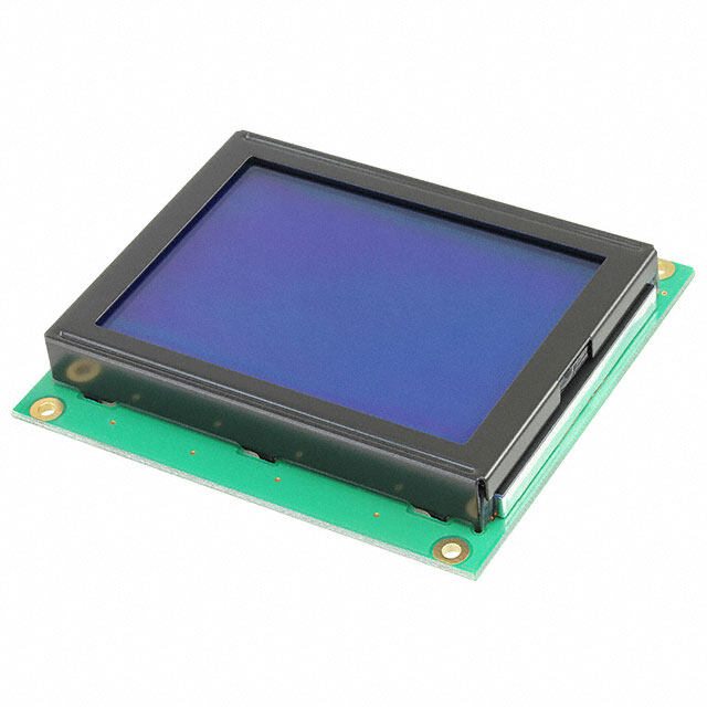
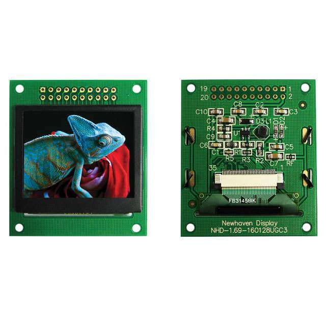
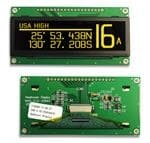
ICGOO电子元器件商城为您提供NHD-3.12-25664UCY2由Newhaven Display设计生产,在icgoo商城现货销售,并且可以通过原厂、代理商等渠道进行代购。 NHD-3.12-25664UCY2价格参考。Newhaven DisplayNHD-3.12-25664UCY2封装/规格:智能,智慧,发光二极管,显示器,图形, 图形 LCD 显示模块 黄色 OLED - 无源矩阵 并联,8 位,SPI 3.12"(79.25mm) 256 x 64。您可以下载NHD-3.12-25664UCY2参考资料、Datasheet数据手册功能说明书,资料中有NHD-3.12-25664UCY2 详细功能的应用电路图电压和使用方法及教程。
| 参数 | 数值 |
| 产品目录 | |
| 描述 | LCD OLED GRAPHIC 256 X 64 YLWOLED显示器和配件 OLED 256 x 64 Yellow 89.2 x 44.0 x 6.0 |
| 产品分类 | |
| 品牌 | Newhaven Display |
| 产品手册 | |
| 产品图片 |
|
| rohs | 符合RoHS无铅 / 符合限制有害物质指令(RoHS)规范要求 |
| 产品系列 | OLED显示器和配件,Newhaven Display NHD-3.12-25664UCY2- |
| 数据手册 | |
| 产品型号 | NHD-3.12-25664UCY2 |
| 产品 | OLED Display Modules |
| 产品培训模块 | http://www.digikey.cn/PTM/IndividualPTM.page?site=cn&lang=zhs&ptm=25399 |
| 产品种类 | OLED显示器和配件 |
| 其它名称 | NHD31225664UCY2 |
| 其它有关文件 | |
| 分辨率 | 256 x 64 |
| 可视范围 | 82.00mm 长 x 22.00mm 宽 |
| 商标 | Newhaven Display |
| 屏幕对角线尺寸 | 3.12" (79.25mm) |
| 工作电流 | 146 mA |
| 工作电源电压 | 2.95 V |
| 接口 | 8 bit Parallel/3-Wire SPI or 4-Wire SPI |
| 文字颜色 | 黄 |
| 显示模式 | 无源 |
| 显示类型 | OLED |
| 显示角 | 80 deg |
| 最大工作温度 | + 85 C |
| 最小工作温度 | - 40 C |
| 标准包装 | 50 |
| 点像素 | 256 x 64 |
| 点尺寸 | 0.28mm x 0.28mm |
| 点间距 | - |
| 照明颜色 | Yellow |
| 背光 | 无背光 |
| 背景颜色 | 黑 |
| 观察区域-宽x高 | 82 mm x 22 mm |






- 商务部:美国ITC正式对集成电路等产品启动337调查
- 曝三星4nm工艺存在良率问题 高通将骁龙8 Gen1或转产台积电
- 太阳诱电将投资9.5亿元在常州建新厂生产MLCC 预计2023年完工
- 英特尔发布欧洲新工厂建设计划 深化IDM 2.0 战略
- 台积电先进制程称霸业界 有大客户加持明年业绩稳了
- 达到5530亿美元!SIA预计今年全球半导体销售额将创下新高
- 英特尔拟将自动驾驶子公司Mobileye上市 估值或超500亿美元
- 三星加码芯片和SET,合并消费电子和移动部门,撤换高东真等 CEO
- 三星电子宣布重大人事变动 还合并消费电子和移动部门
- 海关总署:前11个月进口集成电路产品价值2.52万亿元 增长14.8%

/VM800B35A-BK.jpg)

PDF Datasheet 数据手册内容提取
NHD-3.12-25664UCY2 Graphic OLED Display Module NHD- Newhaven Display 3.12- 3.12” diagonal size 25664- 256 x 64 pixel resolution UC- Model Y- Emitting Color: Yellow 2- +2.95V power supply Newhaven Display International, Inc. 2661 Galvin Ct. Elgin IL, 60124 Ph: 847-844-8795 Fax: 847-844-8796 www.newhavendisplay.com nhtech@newhavendisplay.com nhsales@newhavendisplay.com
Document Revision History Revision Date Description Changed by 0 5/1/2011 Initial Product Release - 1 2/22/2013 Electrical characteristics and mechanical drawing updated JN 2 5/2/16 Supply Current Updated SB Functions and Features • 256 x 64 pixel resolution • Built-in SSD1322 controller • Parallel or serial MPU interface • Single, low voltage power supply • RoHS compliant [2]
Mechanical Drawing L 1 2 3 4 5 6 Rev Description A Date I A A T N E B D B I F N C C O C D D Date 02/22/13 Gen. Tolerance Unit Model: ±0.3mm mm NHD-3.12-25664UCY2 1 2 3 4 5 6 The drawing contained herein is the exclusive property of Newhaven Display International, Inc. and shall not be copied, reproduced, and/or disclosed in any format without permission. [3]
Interface Description Parallel Interface: Pin No. Symbol External Function Description Connection 1 VSS Power Supply Ground 2 VDD Power Supply Supply Voltage for OLED and logic. 3 NC - No Connect 4 D/C MPU Register select signal. D/C=0: Command, D/C=1: Data 5 R/W or /WR MPU 6800-interface: Read/Write select signal, R/W=1: Read R/W: =0: Write 8080-interface: Active LOW Write signal. 6 E or /RD MPU 6800-interface: Operation enable signal. Falling edge triggered. 8080-interface: Active LOW Read signal. 7-14 DB0 – DB7 MPU 8-bit Bi-directional data bus lines. 15 NC - No Connect 16 /RES MPU Active LOW Reset signal. 17 /CS MPU Active LOW Chip Select signal. 18 NC - No Connect 19 BS1 MPU MPU Interface Select signal. 20 BS0 MPU MPU Interface Select signal. Serial Interface: Pin No. Symbol External Function Description Connection 1 VSS Power Supply Ground 2 VDD Power Supply Supply Voltage for OLED and logic. 3 NC - No Connect 4 D/C MPU Register select signal. D/C=0: Command, D/C=1: Data Tie LOW for 3-wire Serial Interface. 5-6 VSS Power Supply Ground 7 SCLK MPU Serial Clock signal. 8 SDIN MPU Serial Data Input signal. 9 NC - No Connect 10-14 VSS Power Supply Ground 15 NC - No Connect 16 /RES MPU Active LOW Reset signal. 17 /CS MPU Active LOW Chip Select signal. 18 NC - No Connect 19 BS1 MPU MPU Interface Select signal. 20 BS0 MPU MPU Interface Select signal. MPU Interface Pin Selections 3-wire 4-wire Pin 6800 Parallel 8080 Parallel Serial Serial Name 8-bit interface 8-bit interface Interface Interface BS1 1 1 0 0 BS0 1 0 1 0 [4]
MPU Interface Pin Assignment Summery Bus Data/Command Interface Control Signals Interface D7 D6 D5 D4 D3 D2 D1 D0 E R/W /CS D/C /RES 8-bit 6800 D[7:0] E R/W /CS D/C /RES 8-bit 8080 D[7:0] /RD /WR /CS D/C /RES 3-wire SPI Tie LOW NC SDIN SCLK Tie LOW /CS Tie LOW /RES 4-wire SPI Tie LOW NC SDIN SCLK Tie LOW /CS D/C /RES Wiring Diagrams [5]
Electrical Characteristics Item Symbol Condition Min. Typ. Max. Unit Operating Temperature Range Top Absolute Max -40 - +85 ⁰C Storage Temperature Range Tst Absolute Max -40 - +90 ⁰C Supply Voltage VDD - - 3.0 3.3 V Supply Current (logic) IDD Ta=25°C - 5 6 mA 50% ON - 146 155 mA Supply Current (display) ICC 100% ON - 239 255 mA Sleep Mode Current IDD+ICC - - - 110 µA SLEEP “H” Level input Vih - 0.8*VDD - VDD V “L” Level input Vil - VSS - 0.2*VDD V “H” Level output Voh - 0.9*VDD - VDD V “L” Level output Vol - VSS - 0.1*VDD V Optical Characteristics Item Symbol Condition Min. Typ. Max. Unit Top ϕY+ - 80 - ⁰ Optimal Bottom ϕY- - 80 - ⁰ Viewing Left θX- - 80 - ⁰ Angles Right θX+ - 80 - ⁰ Contrast Ratio Cr - 2000:1 - - - Rise Tr - - 10 - us Response Time Fall Tf - - 10 - us Brightness - 50% checkerboard 60 80 - cd/m2 Lifetime - Ta=25°C, 50% 40,000 - - Hrs checkerboard Note: Lifetime at typical temperature is based on accelerated high-temperature operation. Lifetime is tested at average 50% pixels on and is rated as Hours until Half-Brightness. The Display OFF command can be used to extend the lifetime of the display. Luminance of active pixels will degrade faster than inactive pixels. Residual (burn-in) images may occur. To avoid this, every pixel should be illuminated uniformly. [6]
Built-in SSD1322 controller Instruction Table Code RESET Instruction Description D/C HEX DB7 DB6 DB5 DB4 DB3 DB2 DB1 DB0 value Enable Grayscale 0 00 0 0 0 0 0 0 0 0 Enable the Grayscale table settings. (see command 0xB8) Table Set Column 0 15 0 0 0 1 0 1 0 1 Set column start and end address Address 1 A[6:0] * A6 A5 A4 A3 A2 A1 A0 A[6:0]: Column start address. Range: 0-119d 0 1 B[6:0] * B6 B5 B4 B3 B2 B1 B0 B[6:0]: Column end address. Range: 0-119d 119d Write RAM 0 5C 0 1 0 1 1 1 0 0 Enable MCU to write Data into RAM Command Read RAM 0 5D 0 1 0 1 1 1 0 1 Enable MCU to read Data from RAM Command Set Row Address 0 75 0 1 1 1 0 1 0 1 Set row start and end address 1 A[6:0] * A6 A5 A4 A3 A2 A1 A0 A[6:0]: Row start address. Range: 0-127d 0 1 B[6:0] * B6 B5 B4 B3 B2 B1 B0 B[6:0]: Row end address. Range: 0-127d 127d Set Remap 0 A0 1 0 1 0 0 0 0 0 A[0] = 0; Horizontal Address Increment 0 1 A[5:0] 0 0 A5 A4 0 A2 A1 A0 A[0] = 1; Vertical Address Increment 1 B[4] * * 0 B4 0 0 0 1 A[1] = 0; Disable Column Address remap 0 A[1] = 1; Enable Column Address remap A[2] = 0; Disable Nibble remap 0 A[2] = 1; Enable Nibble remap A[4] = 0; Scan from COM0 to COM[N-1] 0 A[4] = 1; Scan from COM[N-1] to COM0 A[5] = 0; Disable COM split Odd/Even 0 A[5] = 1; Enable COM split Odd/Even B[4] = 0; Disable Dual COM mode 0 B[4] = 1; Enable Dual COM mode Note: A[5] must be 0 if B[4] is 1. Set Display Start 0 A1 1 0 1 0 0 0 0 1 Set display RAM display start line register from 0-127. 0 Line 1 A[6:0] * A6 A5 A4 A3 A2 A1 A0 Set Display Offset 0 A2 1 0 1 0 0 0 1 0 Set vertical shift by COM from 0~127. 0 1 A[6:0] * A6 A5 A4 A3 A2 A1 A0 Display Mode 0 A4/A7 1 0 1 0 0 X2 X1 X0 0xA4 = Entire display OFF 0xA6 0xA5 = Entire display ON, all pixels Grayscale level 15 0xA6 = Normal display 0xA7 = Inverse display Enable Partial 0 A8 1 0 1 0 1 0 0 0 Turns ON partial mode. Display 1 A[6:0] 0 A6 A5 A4 A3 A2 A1 A0 A[6:0] = Address of start row 1 B[6:0] 0 B6 B5 B4 B3 B2 B1 B0 B[6:0] = Address of end row (B[6:0] > A[6:0]) [7]
Exit Partial Display 0 A9 1 0 1 0 1 0 0 1 Exit Partial Display mode Function Selection 0 AB 1 0 1 0 1 0 1 1 A[0] = 0; External VDD 1 A[0] 0 0 0 0 0 0 0 A0 A[0] = 1; Internal VDD regulator 1 Set Sleep Mode 0 AE~AF 1 0 1 0 1 1 1 X0 0xAE = Sleep Mode ON (display OFF) ON/OFF 0xAF = Sleep Mode OFF (display ON) Set Phase Length 0 B1 1 0 1 1 0 0 0 1 A[3:0] = P1. Phase 1 period of 5-31 DCLK clocks 9 1 A[7:0] A7 A6 A5 A4 A3 A2 A1 A0 A[7:4] = P2. Phase 2 period of 3-15 DCLK clocks 7 Set Display Clock 0 B3 1 0 1 1 0 0 1 1 A[3:0] = 0000; divide by 1 0 Divide Ratio / 1 A[7:0] A7 A6 A5 A4 A3 A2 A1 A0 A[3:0] = 0001; divide by 2 Oscillator A[3:0] = 0010; divide by 4 A[3:0] = 0011; divide by 8 Frequency A[3:0] = 0100; divide by 16 A[3:0] = 0101; divide by 32 A[3:0] = 0110; divide by 64 A[3:0] = 0111; divide by 128 A[3:0] = 1000; divide by 256 A[3:0] = 1001; divide by 512 A[3:0] = 1010; divide by 1024 A[3:0] >= 1011; invalid 1100b A[7:4] = Set the Oscillator Frequency. Frequency increases with the value of A[7:4]. Range 0000b~1111b. Set GPIO 0 B5 1 0 1 1 0 1 0 1 A[1:0] = 00; GPIO0 input disabled 1 A[3:0] * * * * A3 A2 A1 A0 A[1:0] = 01; GPIO0 input enabled A[1:0] = 10; GPIO0 output LOW 10b A[1:0] = 11; GPIO0 output HIGH A[3:2] = 00; GPIO1 input disabled A[3:2] = 01; GPIO1 input enabled A[3:2] = 10; GPIO1 output LOW 10b A[3:2] = 11; GPIO1 output HIGH Set Second 0 B6 1 0 1 1 0 1 1 0 Sets the second precharge period 1000b Precharge Period 1 A[3:0] * * * * A3 A2 A1 A0 A[3:0] = DCLKs Set Grayscale 0 B8 1 0 1 1 1 0 0 0 Sets the gray scale pulse width in units of DCLK. Range 0-180d. Table 1 A1[7:0] A1 A1 A1 A1 A1 A1 A1 A1 A1[7:0] = Gamma Setting for GS1 7 6 5 4 3 2 1 0 1 A2[7:0] A2 A2 A2 A2 A2 A2 A2 A2 A2[7:0] = Gamma Setting for GS2 7 6 5 4 3 2 1 0 1 . . . . . . . . . . 1 . . . . . . . . . . . 1 . . . . . . . . . A14[7:0] = Gamma Setting for GS14 1 A14[7:0] A14 A14 A14 A14 A14 A14 A14 A14 7 6 5 4 3 2 1 0 A15[7:0] = Gamma Setting for GS15 1 A15[7:0] A15 A15 A15 A15 A15 A15 A15 A15 7 6 5 4 3 2 1 0 Note: 0 < GS1 < GS2 < GS3 … < GS14 < GS15 The setting must be followed by command 0x00. Select Default 0 B9 1 0 1 1 1 0 0 1 Sets Linear Grayscale table [8]
Linear Gray Scale GS0 pulse width = 0 Table GS0 pulse width = 0 GS0 pulse width = 8 GS0 pulse width = 16 . . . GS0 pulse width = 104 GS0 pulse width = 112 Set Precharge 0 BB 1 0 1 1 1 0 1 1 Set precharge voltage level. 0x17 Voltage 1 A[4:0] * * * A4 A3 A2 A1 A0 A[4:0] = 0x00; 0.20*VCC . . A[4:0] = 0x3E; 0.60*VCC Set VCOMH 0 BE 1 0 1 1 1 1 1 0 Sets the VCOMH voltage level 0x04 Voltage 1 A[3:0] * * * * A3 A2 A1 A0 A[3:0] = 0x00; 0.72*VCC . . A[3:0] = 0x04; 0.8*VCC . . A[3:0] = 0x07; 0.86*VCC Set Contrast 0 C1 1 1 0 0 0 0 0 1 Double byte command to select 1 out of 256 contrast steps. 0x7F Control 1 A[7:0] A7 A6 A5 A4 A3 A2 A1 A0 Contrast increases as the value increases. Master Contrast 0 C7 1 1 0 0 0 1 1 1 A[3:0] = 0x00; Reduce output for all colors to 1/16 0x0f Control 1 A[3:0] * * * * A3 A2 A1 A0 A[3:0] = 0x01; Reduce output for all colors to 2/16 . . A[3:0] = 0x0E; Reduce output for all colors to 15/16 A[3:0] = 0x0F; no change Set Multiplex 0 CA 1 1 0 0 1 0 1 0 Set MUX ratio to N+1 MUX 127d Ratio 1 A[6:0] * A6 A5 A4 A3 A2 A1 A0 N=A[6:0]; from 16MUX to 128MUX (0 to 14 are invalid) Set Command 0 FD 1 1 1 1 1 1 0 1 A[2] = 0; Unlock OLED to enable commands 0x12 Lock 1 A[2] 0 0 0 1 0 A2 1 0 A[2] = 1; Lock OLED from entering commands For detailed instruction information, see datasheet: http://www.newhavendisplay.com/app_notes/SSD1322.pdf [9]
MPU Interface For detailed timing information, see datasheet: http://www.newhavendisplay.com/app_notes/SSD1322.pdf 6800-MPU Parallel Interface The parallel interface consists of 8 bi-directional data pins, R/W, D/C, E, and /CS. A LOW on R/W indicates write operation, and HIGH on R/W indicates read operation. A LOW on D/C indicates “Command” read or write, and HIGH on D/C indicates “Data” read or write. The E input serves as data latch signal, while /CS is LOW. Data is latched at the falling edge of E signal. Function E R/W /CS D/C Write Command ↓ 0 0 0 Read Status ↓ 1 0 0 Write Data ↓ 0 0 1 Read Data ↓ 1 0 1 8080-MPU Parallel Interface The parallel interface consists of 8 bi-directional data pins, /RD, /WR, D/C, and /CS. A LOW on D/C indicates “Command” read or write, and HIGH on D/C indicates “Data” read or write. A rising edge of /RS input serves as a data read latch signal while /CS is LOW. A rising edge of /WR input serves as a data/command write latch signal while /CS is LOW. Function /RD /WR /CS D/C Write Command 1 ↑ 0 0 Read Status ↑ 1 0 0 Write Data 1 ↑ 0 1 Read Data ↑ 1 0 1 Alternatively, /RD and /WR can be kept stable while /CS serves as the data/command latch signal. Function /RD /WR /CS D/C Write Command 1 0 ↑ 0 Read Status 0 1 ↑ 0 Write Data 1 0 ↑ 1 Read Data 0 1 ↑ 1 [10]
Serial Interface (4-wire) The 4-wire serial interface consists of serial clock SCLK, serial data SDIN, D/C, and /CS. D0 acts as SCLK and D1 acts as SDIN. D2 should be left open. D3~D7, E, and R/W should be connected to GND. Function /RD /WR /CS D/C D0 Write Command Tie LOW Tie LOW 0 0 ↑ Write Data Tie LOW Tie LOW 0 1 ↑ SDIN is shifted into an 8-bit shift register on every rising edge of SCLK in the order of D7, D6,…D0. D/C is sampled on every eighth clock and the data byte in the shift register is written to the GDRAM or command register in the same clock. Note: Read is not available in serial mode. Serial Interface (3-wire) The 3-wire serial interface consists of serial clock SCLK, serial data SDIN, and /CS. D0 acts as SCLK and D1 acts as SDIN. D2 should be left open. D3~D7, E, R/W, and D/C should be connected to GND. Function /RD /WR /CS D/C D0 Write Command Tie LOW Tie LOW 0 Tie LOW ↑ Write Data Tie LOW Tie LOW 0 Tie LOW ↑ SDIN is shifted into an 9-bit shift register on every rising edge of SCLK in the order of D/C, D7, D6,…D0. D/C (first bit of the sequential data) will determine if the following data byte is written to the Display Data RAM (D/C = 1) or the command register (D/C = 0). Note: Read is not available in serial mode. For detailed protocol information, see datasheet: http://www.newhavendisplay.com/app_notes/SSD1322.pdf [11]
Example Initialization Sequence: Set_Command_Lock(0x12); // Unlock Basic Commands (0x12/0x16) Set_Display_On_Off(0x00); // Display Off (0x00/0x01) Set_Column_Address(0x1C,0x5B); Set_Row_Address(0x00,0x3F); Set_Display_Clock(0x91); // Set Clock as 80 Frames/Sec Set_Multiplex_Ratio(0x3F); // 1/64 Duty (0x0F~0x3F) Set_Display_Offset(0x00); // Shift Mapping RAM Counter (0x00~0x3F) Set_Start_Line(0x00); // Set Mapping RAM Display Start Line (0x00~0x7F) Set_Remap_Format(0x14); // Set Horizontal Address Increment // Column Address 0 Mapped to SEG0 // Disable Nibble Remap // Scan from COM[N-1] to COM0 // Disable COM Split Odd Even // Enable Dual COM Line Mode Set_GPIO(0x00); // Disable GPIO Pins Input Set_Function_Selection(0x01); // Enable Internal VDD Regulator Set_Display_Enhancement_A(0xA0,0xFD); // Enable External VSL Set_Contrast_Current(0x9F); // Set Segment Output Current Set_Master_Current(0x0F); // Set Scale Factor of Segment Output Current Control //Set_Gray_Scale_Table(); // Set Pulse Width for Gray Scale Table Set_Linear_Gray_Scale_Table(); //set default linear gray scale table Set_Phase_Length(0xE2); // Set Phase 1 as 5 Clocks & Phase 2 as 14 Clocks Set_Display_Enhancement_B(0x20); // Enhance Driving Scheme Capability (0x00/0x20) Set_Precharge_Voltage(0x1F); // Set Pre-Charge Voltage Level as 0.60*VCC Set_Precharge_Period(0x08); // Set Second Pre-Charge Period as 8 Clocks Set_VCOMH(0x07); // Set Common Pins Deselect Voltage Level as 0.86*VCC Set_Display_Mode(0x02); // Normal Display Mode (0x00/0x01/0x02/0x03) Set_Partial_Display(0x01,0x00,0x00); // Disable Partial Display Set_Display_On_Off(0x01); [12]
Quality Information Test Item Content of Test Test Condition Note High Temperature storage Test the endurance of the display at high +90⁰C , 240hrs 2 storage temperature. Low Temperature storage Test the endurance of the display at low -40⁰C , 240hrs 1,2 storage temperature. High Temperature Test the endurance of the display by +85⁰C 240hrs 2 Operation applying electric stress (voltage & current) at high temperature. Low Temperature Test the endurance of the display by -40⁰C , 240hrs 1,2 Operation applying electric stress (voltage & current) at low temperature. High Temperature / Test the endurance of the display by +60⁰C , 90% RH , 240hrs 1,2 Humidity Operation applying electric stress (voltage & current) at high temperature with high humidity. Thermal Shock resistance Test the endurance of the display by -40⁰C,30min -> 25⁰C,5min -> applying electric stress (voltage & current) 85⁰C,30min = 1 cycle during a cycle of low and high 100 cycles temperatures. Vibration test Test the endurance of the display by 10-22Hz , 15mm amplitude. 3 applying vibration to simulate 22-500Hz, 1.5G transportation and use. 30min in each of 3 directions X,Y,Z Atmospheric Pressure test Test the endurance of the display by 115mbar, 40hrs 3 applying atmospheric pressure to simulate transportation by air. Static electricity test Test the endurance of the display by VS=800V, RS=1.5kΩ, CS=100pF applying electric static discharge. One time Note 1: No condensation to be observed. Note 2: Conducted after 2 hours of storage at 25⁰C, 0%RH. Note 3: Test performed on product itself, not inside a container. Evaluation Criteria: 1: Display is fully functional during operational tests and after all tests, at room temperature. 2: No observable defects. 3: Luminance >50% of initial value. 4: Current consumption within 50% of initial value Precautions for using OLEDs/LCDs/LCMs See Precautions at www.newhavendisplay.com/specs/precautions.pdf Warranty Information and Terms & Conditions http://www.newhavendisplay.com/index.php?main_page=terms Newhaven Display International, Inc. reserves the right to alter this product or specification at any time without notification. [13]
Mouser Electronics Authorized Distributor Click to View Pricing, Inventory, Delivery & Lifecycle Information: N ewhaven Display: NHD-3.12-25664UCY2
 Datasheet下载

