ICGOO在线商城 > 分立半导体产品 > 晶体管 - UGBT,MOSFET - 单 > NGTB15N60EG
 Datasheet下载
- 型号: NGTB15N60EG
- 制造商: ON Semiconductor
- 库位|库存: xxxx|xxxx
- 要求:
| 数量阶梯 | 香港交货 | 国内含税 |
| +xxxx | $xxxx | ¥xxxx |
查看当月历史价格
查看今年历史价格
NGTB15N60EG产品简介:
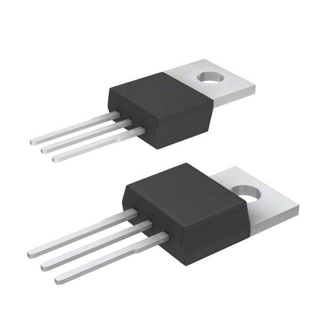
ICGOO电子元器件商城为您提供NGTB15N60EG由ON Semiconductor设计生产,在icgoo商城现货销售,并且可以通过原厂、代理商等渠道进行代购。 NGTB15N60EG价格参考。ON SemiconductorNGTB15N60EG封装/规格:晶体管 - UGBT,MOSFET - 单, IGBT NPT 600V 30A 117W Through Hole TO-220。您可以下载NGTB15N60EG参考资料、Datasheet数据手册功能说明书,资料中有NGTB15N60EG 详细功能的应用电路图电压和使用方法及教程。
| 参数 | 数值 |
| 25°C时Td(开/关)值 | 78ns/130ns |
| 产品目录 | |
| Current-CollectorPulsed(Icm) | 120A |
| 描述 | IGBT 600V 30A 117W TO220-3IGBT 晶体管 15A 600V IGBT |
| 产品分类 | IGBT - 单路分离式半导体 |
| GateCharge | 80nC |
| IGBT类型 | NPT |
| 品牌 | ON Semiconductor |
| 产品手册 | |
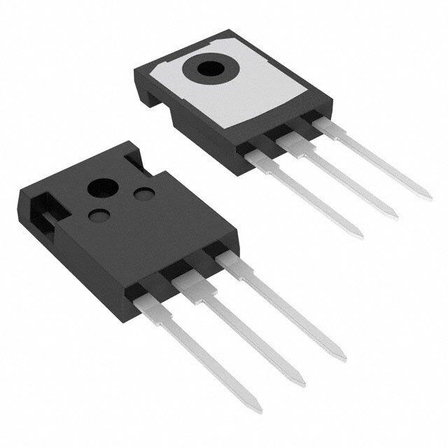
| 产品图片 |
|
| rohs | 符合RoHS无铅 / 符合限制有害物质指令(RoHS)规范要求 |
| 产品系列 | 晶体管,IGBT 晶体管,ON Semiconductor NGTB15N60EG- |
| 数据手册 | |
| 产品型号 | NGTB15N60EG |
| SwitchingEnergy | 900µJ (开), 300µJ (关) |
| TestCondition | 400V,15A,22 欧姆,15V |
| 不同 Vge、Ic时的 Vce(on) | 1.95V @ 15V,15A |
| 产品种类 | IGBT 晶体管 |
| 供应商器件封装 | TO-220 |
| 其它名称 | NGTB15N60EG-ND |
| 功率-最大值 | 117W |
| 功率耗散 | 47 W |
| 包装 | 管件 |
| 反向恢复时间(trr) | 270ns |
| 商标 | ON Semiconductor |
| 在25C的连续集电极电流 | 30 A |
| 安装类型 | 通孔 |
| 安装风格 | Through Hole |
| 封装 | Tube |
| 封装/外壳 | TO-220-3 |
| 封装/箱体 | TO-220 |
| 工厂包装数量 | 50 |
| 栅极/发射极最大电压 | 20 V |
| 栅极—射极漏泄电流 | 100 nA |
| 标准包装 | 50 |
| 电压-集射极击穿(最大值) | 600V |
| 电流-集电极(Ic)(最大值) | 30A |
| 系列 | NGTB15N60EG |
| 输入类型 | 标准 |
| 集电极—发射极最大电压VCEO | 600 V |
| 集电极—射极饱和电压 | 1.95 V |


- 商务部:美国ITC正式对集成电路等产品启动337调查
- 曝三星4nm工艺存在良率问题 高通将骁龙8 Gen1或转产台积电
- 太阳诱电将投资9.5亿元在常州建新厂生产MLCC 预计2023年完工
- 英特尔发布欧洲新工厂建设计划 深化IDM 2.0 战略
- 台积电先进制程称霸业界 有大客户加持明年业绩稳了
- 达到5530亿美元!SIA预计今年全球半导体销售额将创下新高
- 英特尔拟将自动驾驶子公司Mobileye上市 估值或超500亿美元
- 三星加码芯片和SET,合并消费电子和移动部门,撤换高东真等 CEO
- 三星电子宣布重大人事变动 还合并消费电子和移动部门
- 海关总署:前11个月进口集成电路产品价值2.52万亿元 增长14.8%


PDF Datasheet 数据手册内容提取
NGTB15N60EG IGBT - Short-Circuit Rated This Insulated Gate Bipolar Transistor (IGBT) features a robust and cost effective Non−Punch Through (NPT) Trench construction, and provides superior performance in demanding switching applications. Offering both low on state voltage and minimal switching loss, the IGBT is well suited for motor drive control and other hard switching www.onsemi.com applications. Incorporated into the device is a rugged co−packaged reverse recovery diode with a low forward voltage. 15 A, 600 V Features V = 1.7 V CEsat • Low Saturation Voltage Resulting in Low Conduction Loss • Low Switching Loss in Higher Frequency Applications C • Soft Fast Reverse Recovery Diode • 10 (cid:2)s Short Circuit Capability • Excellent Current versus Package Size Performance Density • This is a Pb−Free Device G Typical Applications E • White Goods Appliance Motor Control • General Purpose Inverter • AC and DC Motor Control C ABSOLUTE MAXIMUM RATINGS Rating Symbol Value Unit Collector−emitter voltage VCES 600 V TO−220 CASE 221A Collector current I A @ TC = 25°C C 30 GC STYLE 9 @ TC = 100°C 15 E Pulsed collector current, Tpulse limited by ICM 120 A MARKING DIAGRAM TJmax Diode forward current IF A @ TC = 25°C 30 @ TC = 100°C 15 Diode pulsed current, Tpulse limited by IFM 120 A TJmax 15N60G Gate−emitter voltage VGE (cid:2)20 V AYWW Power dissipation PD W @ TC = 25°C 117 @ TC = 100°C 47 Short circuit withstand time tSC 10 (cid:2)s VGE = 15 V, VCE = 400 V, TJ (cid:3) +150°C Operating junction temperature range TJ −55 to °C A = Assembly Location +150 Y = Year WW = Work Week Storage temperature range Tstg −55 to °C G = Pb−Free Package +150 Lead temperature for soldering, 1/8” from TSLD 260 °C case for 5 seconds ORDERING INFORMATION Stresses exceeding those listed in the Maximum Ratings table may damage the Device Package Shipping device. If any of these limits are exceeded, device functionality should not be assumed, damage may occur and reliability may be affected. NGTB15N60EG TO−220 50 Units / Rail (Pb−Free) © Semiconductor Components Industries, LLC, 2015 1 Publication Order Number: January, 2015 − Rev. 8 NGTB15N60E/D
NGTB15N60EG THERMAL CHARACTERISTICS Rating Symbol Value Unit Thermal resistance junction to case, for IGBT R(cid:3)JC 1.06 °C/W Thermal resistance junction to case, for Diode R(cid:3)JC 3.76 °C/W Thermal resistance junction to ambient R(cid:3)JA 60 °C/W ELECTRICAL CHARACTERISTICS (TJ = 25°C unless otherwise specified) Parameter Test Conditions Symbol Min Typ Max Unit STATIC CHARACTERISTIC Collector−emitter breakdown voltage, VGE = 0 V, IC = 500 (cid:2)A V(BR)CES 600 − − V gate−emitter short−circuited Collector−emitter saturation voltage VGE = 15 V , IC = 15 A VCEsat 1.45 1.7 1.95 V VGE = 15 V , IC = 15 A, TJ = 150°C 1.8 2.1 2.4 Gate−emitter threshold voltage VGE = VCE , IC = 250 (cid:2)A VGE(th) 4.5 5.5 6.5 V Collector−emitter cut−off current, gate−emitter VGE = 0 V, VCE = 600 V ICES − 10 − (cid:2)A short−circuited VGE = 0 V, VCE = 600 V, TJ = 150°C − − 200 Gate leakage current, collector−emitter VGE = 20 V, VCE = 0 V IGES − − 100 nA short−circuited Forward Transconductance VCE = 20 V, IC = 15 A gfs − 10.1 − S DYNAMIC CHARACTERISTIC Input capacitance Cies − 2600 − Output capacitance VCE = 20 V, VGE = 0 V, f = 1 MHz Coes − 64 − pF Reverse transfer capacitance Cres − 42 − Gate charge total Qg − 80 − Gate to emitter charge VCE = 480 V, IC = 15 A, VGE = 15 V Qge − 24 − nC Gate to collector charge Qgc − 33 − SWITCHING CHARACTERISTIC , INDUCTIVE LOAD Turn−on delay time td(on) − 78 − Rise time tr − 30 − ns Turn−off delay time TJ = 25°C td(off) − 130 − Fall time VCC = R4g0 0= V2,2 I C(cid:4) = 15 A tf − 120 − Turn−on switching loss VGE = 0 V / 15 V Eon − 0.900 − Turn−off switching loss Eoff − 0.300 − mJ Total switching loss Ets − 1.200 − Turn−on delay time td(on) − 76 − Rise time tr − 33 − ns Turn−off delay time TJ = 150°C td(off) − 133 − Fall time VCC = R40g 0= V2,2 I C(cid:4) = 15 A tf − 223 − Turn−on switching loss VGE = 0 V / 15 V Eon − 1.10 − Turn−off switching loss Eoff − 0.510 − mJ Total switching loss Ets − 1.610 − DIODE CHARACTERISTIC Forward voltage VGE = 0 V, IF = 15 A VF − 1.6 1.85 V VGE = 0 V, IF = 15 A, TJ = 150°C − 1.6 − www.onsemi.com 2
NGTB15N60EG ELECTRICAL CHARACTERISTICS (TJ = 25°C unless otherwise specified) Parameter Test Conditions Symbol Min Typ Max Unit DIODE CHARACTERISTIC Reverse recovery time TJ = 25°C trr − 270 − ns Reverse recovery charge IF = 15 A, VR = 200 V Qrr − 350 − nc diF/dt = 200 A/µs Reverse recovery current Irrm − 5 − A Reverse recovery time TJ = 125°C trr − 350 − ns Reverse recovery charge IF = 15 A, VR = 200 V Qrr − 1000 − nc diF/dt = 200 A/µs Reverse recovery current Irrm − 7.5 − A Product parametric performance is indicated in the Electrical Characteristics for the listed test conditions, unless otherwise noted. Product performance may not be indicated by the Electrical Characteristics if operated under different conditions. www.onsemi.com 3
NGTB15N60EG TYPICAL CHARACTERISTICS 60 60 TJ = 25°C TJ = 150°C NT (A) 50 VGE = 17 V to 13 V NT (A) 50 VGE = 17 V to 15 V 13 V E E R 40 R 40 R R U U C C R 30 11 V R 30 O O 11 V T T C C E 20 E 20 L L L L CO 10 9 V CO 10 9 V , C , C I I 7 V 0 7 V 0 0 1 2 3 4 5 6 7 8 0 1 2 3 4 5 6 7 8 9 VCE, COLLECTOR−EMITTER VOLTAGE (V) VCE, COLLECTOR−EMITTER VOLTAGE (V) Figure 1. IGBT Output Characteristics Figure 2. IGBT Output Characteristics 60 60 TJ = −40°C VCE = 20 V T (A) 50 VGE = 17 V to 13 V T (A) 50 TJ = −40°C N N E E RR 40 RR 40 25°C U U R C 30 11 V R C 30 O O T T 150°C C C E 20 E 20 L L L L O O , CC 10 9 V , CC 10 I I 7 V 0 0 0 1 2 3 4 5 6 7 8 0 4 8 12 16 VCE, COLLECTOR−EMITTER VOLTAGE (V) VGE, GATE−EMITTER VOLTAGE (V) Figure 3. IGBT Output Characteristics Figure 4. Typical Transfer Characteristics V) 3.5 10000 E ( VGE = 0 V, G f = 1 MHz TA 3 Cies OL IC = 30 A V 2.5 F) ER IC = 15 A E (p 1000 T 2 C T N MI A E T − 1.5 CI R A O IC = 5 A P 100 LECT 1 IC = 10 A CA Coes OL 0.5 Cres C , CE 0 10 V −60 −40 −20 0 20 40 60 80 100 120 140 160 0 10 20 30 40 50 60 70 80 90 100 TJ, JUNCTION TEMPERATURE (°C) VCE, COLLECTOR−EMITTER VOLTAGE (V) Figure 5. V vs. T Figure 6. Typical Capacitance CE(sat) J www.onsemi.com 4
NGTB15N60EG TYPICAL CHARACTERISTICS 35 20 −40°C V) IC = 15 A A) 30 GE ( ENT ( 25 25°C OLTA 15 VCES = 120 V R V UR 20 R VCES = 480 V RD C 15 MITTE 10 WA 150°C −E R 10 E I, FOF 5 , GATE 5 G V 0 0 0 0.5 1 1.5 2 2.5 0 20 40 60 80 100 VF, FORWARD VOLTAGE (V) QG, GATE CHARGE (nC) Figure 8. Typical Gate Charge Figure 7. Diode Forward Characteristics 1.2 1000 1 Eoff tf mJ) ns) td(off) S ( 0.8 E (100 td(on) S M G LO 0.6 G TI tr N N WITCHI 0.4 Eon VCE = 400 V WITCHI 10 VCE = 400 V S 0.2 VGE = 15 V S VGE = 15 V RICg = = 1 252 A (cid:4) IRCg = = 1 252 A (cid:4) 0 1 0 20 40 60 80 100 120 140 160 0 20 40 60 80 100 120 140 160 180 200 TJ, JUNCTION TEMPERATURE (°C) TJ, JUNCTION TEMPERATURE (°C) Figure 9. Switching Loss vs. Temperature Figure 10. Switching Time vs. Temperature 3 1000 VCE = 400 V VGE = 15 V tf mJ) TRJg == 12520 (cid:4)°C Eon ns) td(off) S ( 2 E (100 td(on) S M O TI G L G tr N HIN CHI WITC 1 Eoff WIT 10 VCE = 400 V S S VGE = 15 V TJ = 150°C Rg = 22 (cid:4) 0 1 8 12 16 20 24 28 32 8 12 16 20 24 28 32 IC, COLLECTOR CURRENT (A) IC, COLLECTOR CURRENT (A) Figure 11. Switching Loss vs. I Figure 12. Switching Time vs. I C C www.onsemi.com 5
NGTB15N60EG TYPICAL CHARACTERISTICS 2 1000 VCE = 400 V S (mJ) 1.6 VTICJG ==E 1=15 51 0A5° CV Eon E (ns) 100 td(otfff) td(otrn) S 1.2 M G LO G TI N N HI 0.8 HI WITC Eoff WITC 10 VCE = 400 V S 0.4 S VGE = 15 V IC = 15 A TJ = 150°C 0 1 5 15 25 35 45 55 65 75 85 5 15 25 35 45 55 65 75 85 Rg, GATE RESISTOR ((cid:4)) Rg, GATE RESISTOR ((cid:4)) Figure 13. Switching Loss vs. Rg Figure 14. Switching Time vs. Rg 2 1000 VGE = 15 V IC = 15 A NERGY (mJ) 11..62 RTJg == 12520 (cid:4)°C Eon G TIME (ns) 100 tr tdt(fon) td(off) E NG 0.8 HIN CHI Eoff WITC 10 SWIT 0.4 S VICG =E 1=5 1 A5 V Rg = 22 (cid:4) TJ = 150°C 0 1 175 225 275 325 375 425 475 525 575 175 225 275 325 375 425 475 525 575 VCE, COLLECTOR−EMITTER VOLTAGE (V) VCE, COLLECTOR−EMITTER VOLTAGE (V) Figure 15. Switching Loss vs. V Figure 16. Switching Time vs. CE Collector−Emitter Voltage 1000 1000 A) 1 ms 100 (cid:2)s A) T ( 100 T ( 100 N N E E R R R 50 (cid:2)s R U 10 U 10 R C dc operation R C O O CT 1 CT 1 E Single Nonrepetitive E L L OL Pulse TC = 25°C OL C 0.1 Curves must be derated C 0.1 , C linearly with increase , C I in temperature I VGE = 15 V, TC = 125°C 0.01 0.01 1 10 100 1000 1 10 100 1000 VCE, COLLECTOR−EMITTER VOLTAGE (V) VCE, COLLECTOR−EMITTER VOLTAGE (V) Figure 17. Safe Operating Area Figure 18. Reverse Bias Safe Operating Area www.onsemi.com 6
NGTB15N60EG TYPICAL CHARACTERISTICS 10 E (Z)(cid:3)JC 1 50% Duty Cycle R(cid:3)JC = 1.06 Ri (°C/W) (cid:5)i (sec) S 20% 0.1 7.1E−5 ON 10% JunctionR1 R2 Rn Case 0.05010 1.0E−4 P 0.1 0.15051 0.002 AL RES 52%% Ci = (cid:5)i/Ri 000...231300950295020 0.000.0.00903939 RM 0.01 1% C1 C2 Cn 0.11423 0.1 E TH Single Pulse Duty Factor = t1/t2 Peak TJ = PDM x Z(cid:3)JC + TC 0.001 0.000001 0.00001 0.0001 0.001 0.01 0.1 1 10 100 1000 PULSE TIME (sec) Figure 19. IGBT Transient Thermal Impedance 10 )C 50% Duty Cycle R(cid:3)JC = 3.76 J Z(cid:3) 1 20% E ( 10% Ri (°C/W) (cid:5)i (sec) ONS 25%% Duty Factor = t1/t2 00..0041089975 11..00EE−−67 SP 0.1 1% Peak TJ = PDM x Z(cid:3)JC + TC 0.102.9156 17..01EE−−55 E L R Single Pulse JunctionR1 R2 Rn Case 01..2602179390 10.0.0E0−24 A M 0.57301 0.003 ER 0.01 Ci = (cid:5)i/Ri 0.45453 0.00498 H 0.40199 0.03 T C1 C2 Cn 0.21558 0.1 0.001 0.000001 0.00001 0.0001 0.001 0.01 0.1 1 10 100 1000 PULSE TIME (sec) Figure 20. Diode Transient Thermal Impedance Figure 21. Test Circuit for Switching Characteristics www.onsemi.com 7
NGTB15N60EG Figure 22. Definition of Turn On Waveform www.onsemi.com 8
NGTB15N60EG Figure 23. Definition of Turn Off Waveform www.onsemi.com 9
NGTB15N60EG PACKAGE DIMENSIONS TO−220 CASE 221A−09 ISSUE AH NOTES: 1. DIMENSIONING AND TOLERANCING PER ANSI Y14.5M, 1982. SEATING −T− PLANE 2. CONTROLLING DIMENSION: INCH. 3. DIMENSION Z DEFINES A ZONE WHERE ALL B F C BODY AND LEAD IRREGULARITIES ARE T S ALLOWED. INCHES MILLIMETERS 4 DIM MIN MAX MIN MAX A 0.570 0.620 14.48 15.75 Q A B 0.380 0.415 9.66 10.53 C 0.160 0.190 4.07 4.83 1 2 3 U D 0.025 0.038 0.64 0.96 F 0.142 0.161 3.61 4.09 H G 0.095 0.105 2.42 2.66 H 0.110 0.161 2.80 4.10 K J 0.014 0.024 0.36 0.61 Z K 0.500 0.562 12.70 14.27 L 0.045 0.060 1.15 1.52 N 0.190 0.210 4.83 5.33 L R Q 0.100 0.120 2.54 3.04 R 0.080 0.110 2.04 2.79 V J S 0.045 0.055 1.15 1.39 T 0.235 0.255 5.97 6.47 G U 0.000 0.050 0.00 1.27 D V 0.045 --- 1.15 --- Z --- 0.080 --- 2.04 N STYLE 9: PIN 1. GATE 2. COLLECTOR 3. EMITTER 4. COLLECTOR ON Semiconductor and are registered trademarks of Semiconductor Components Industries, LLC (SCILLC). SCILLC owns the rights to a number of patents, trademarks, copyrights, trade secrets, and other intellectual property. A listing of SCILLC’s product/patent coverage may be accessed at www.onsemi.com/site/pdf/Patent−Marking.pdf. SCILLC reserves the right to make changes without further notice to any products herein. SCILLC makes no warranty, representation or guarantee regarding the suitability of its products for any particular purpose, nor does SCILLC assume any liability arising out of the application or use of any product or circuit, and specifically disclaims any and all liability, including without limitation special, consequential or incidental damages. “Typical” parameters which may be provided in SCILLC data sheets and/or specifications can and do vary in different applications and actual performance may vary over time. All operating parameters, including “Typicals” must be validated for each customer application by customer’s technical experts. SCILLC does not convey any license under its patent rights nor the rights of others. SCILLC products are not designed, intended, or authorized for use as components in systems intended for surgical implant into the body, or other applications intended to support or sustain life, or for any other application in which the failure of the SCILLC product could create a situation where personal injury or death may occur. Should Buyer purchase or use SCILLC products for any such unintended or unauthorized application, Buyer shall indemnify and hold SCILLC and its officers, employees, subsidiaries, affiliates, and distributors harmless against all claims, costs, damages, and expenses, and reasonable attorney fees arising out of, directly or indirectly, any claim of personal injury or death associated with such unintended or unauthorized use, even if such claim alleges that SCILLC was negligent regarding the design or manufacture of the part. SCILLC is an Equal Opportunity/Affirmative Action Employer. This literature is subject to all applicable copyright laws and is not for resale in any manner. PUBLICATION ORDERING INFORMATION LITERATURE FULFILLMENT: N. American Technical Support: 800−282−9855 Toll Free ON Semiconductor Website: www.onsemi.com Literature Distribution Center for ON Semiconductor USA/Canada P.O. Box 5163, Denver, Colorado 80217 USA Europe, Middle East and Africa Technical Support: Order Literature: http://www.onsemi.com/orderlit Phone: 303−675−2175 or 800−344−3860 Toll Free USA/Canada Phone: 421 33 790 2910 Fax: 303−675−2176 or 800−344−3867 Toll Free USA/Canada Japan Customer Focus Center For additional information, please contact your local Email: orderlit@onsemi.com Phone: 81−3−5817−1050 Sales Representative www.onsemi.com NGTB15N60E/D 10