ICGOO在线商城 > 分立半导体产品 > 晶体管 - 双极 (BJT) - 射频 > NE68119-A
 Datasheet下载
- 型号: NE68119-A
- 制造商: CEL
- 库位|库存: xxxx|xxxx
- 要求:
| 数量阶梯 | 香港交货 | 国内含税 |
| +xxxx | $xxxx | ¥xxxx |
查看当月历史价格
查看今年历史价格
NE68119-A产品简介:
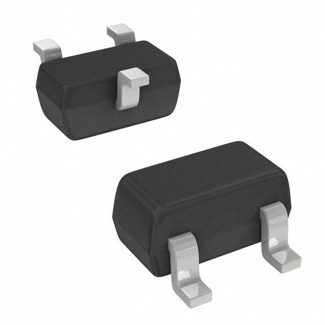
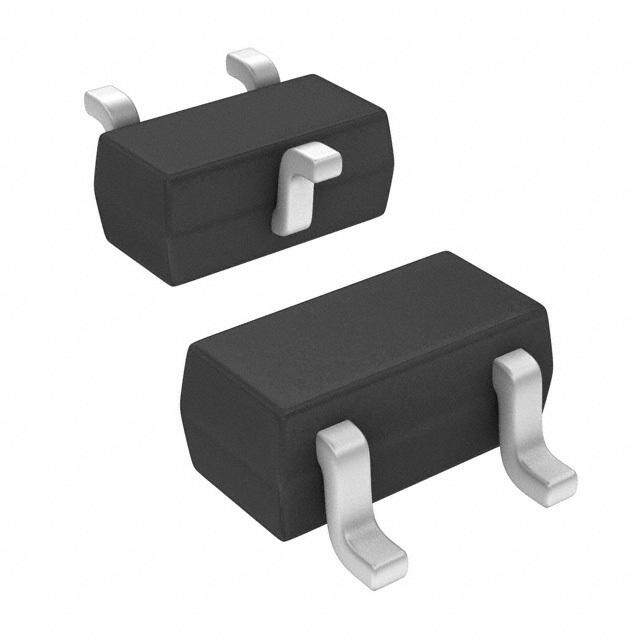
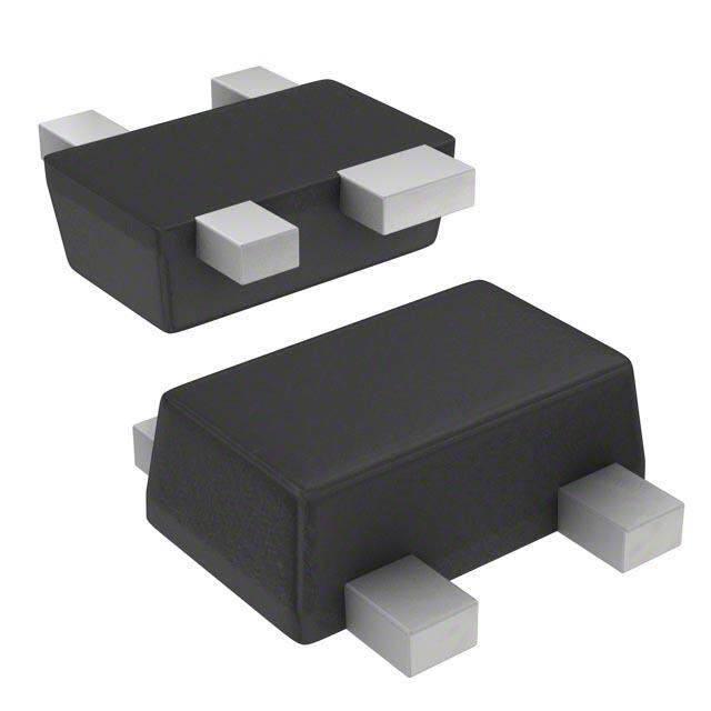
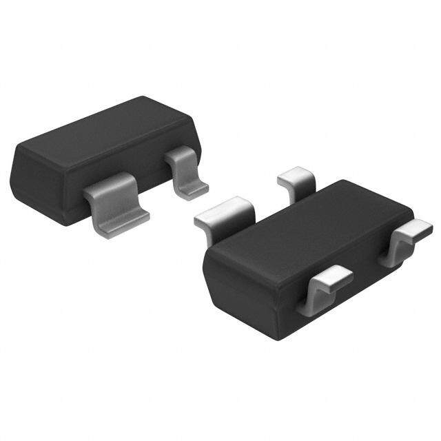
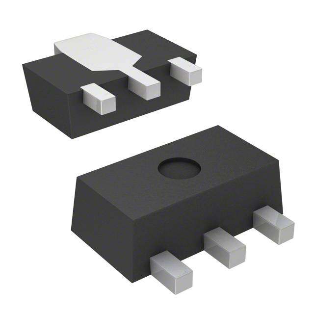
ICGOO电子元器件商城为您提供NE68119-A由CEL设计生产,在icgoo商城现货销售,并且可以通过原厂、代理商等渠道进行代购。 NE68119-A价格参考。CELNE68119-A封装/规格:晶体管 - 双极 (BJT) - 射频, RF Transistor NPN 10V 65mA 7GHz 100mW Surface Mount SOT-523。您可以下载NE68119-A参考资料、Datasheet数据手册功能说明书,资料中有NE68119-A 详细功能的应用电路图电压和使用方法及教程。
型号为NE68119-A、品牌为CEL的双极型射频晶体管主要应用于射频(RF)信号放大和处理电路中。该器件适用于通信设备中的低噪声放大器(LNA)、射频混频器、频率转换模块以及无线基础设施中的前端电路。由于其良好的高频特性和低噪声性能,NE68119-A常用于微波通信、卫星通信、雷达系统和测试测量仪器等高频应用场景。此外,该晶体管也可用于需要高线性度和高稳定性的射频功率放大电路中,适用于工作频率在GHz级别的现代无线通信系统。
| 参数 | 数值 |
| 产品目录 | |
| 描述 | TRANSISTOR NPN 1GHZ SMD |
| 产品分类 | RF 晶体管 (BJT) |
| 品牌 | CEL |
| 数据手册 | |
| 产品图片 |
|
| 产品型号 | NE68119-A |
| rohs | 无铅 / 符合限制有害物质指令(RoHS)规范要求 |
| 产品系列 | - |
| 不同 Ic、Vce 时的DC电流增益(hFE)(最小值) | 80 @ 7mA,3V |
| 供应商器件封装 | 3 针 SuperMiniMold (19) |
| 其它名称 | NE68119A |
| 功率-最大值 | 100mW |
| 包装 | 散装 |
| 噪声系数(dB,不同f时的典型值) | 1.4dB ~ 1.8dB @ 1GHz ~ 2GHz |
| 增益 | 10dB ~ 14dB |
| 安装类型 | 表面贴装 |
| 封装/外壳 | SOT-523 |
| 晶体管类型 | NPN |
| 标准包装 | 1 |
| 电压-集射极击穿(最大值) | 10V |
| 电流-集电极(Ic)(最大值) | 65mA |
| 频率-跃迁 | 7GHz |


- 商务部:美国ITC正式对集成电路等产品启动337调查
- 曝三星4nm工艺存在良率问题 高通将骁龙8 Gen1或转产台积电
- 太阳诱电将投资9.5亿元在常州建新厂生产MLCC 预计2023年完工
- 英特尔发布欧洲新工厂建设计划 深化IDM 2.0 战略
- 台积电先进制程称霸业界 有大客户加持明年业绩稳了
- 达到5530亿美元!SIA预计今年全球半导体销售额将创下新高
- 英特尔拟将自动驾驶子公司Mobileye上市 估值或超500亿美元
- 三星加码芯片和SET,合并消费电子和移动部门,撤换高东真等 CEO
- 三星电子宣布重大人事变动 还合并消费电子和移动部门
- 海关总署:前11个月进口集成电路产品价值2.52万亿元 增长14.8%


PDF Datasheet 数据手册内容提取
DATA SHEET SILICON TRANSISTOR 2SC5007 NE68119 / JEITA Part No. T NPN SILICON EPITAXIAL TRANSISTOR 3 PINS ULTRA SUPER MINI MOLD U DESCRIPTION The NE68119 / 2SC5007 is an NPN epitaxial silicon transistor designed for use in low noise and small signal amplifiers from VHF band to UHF band. Low noise figure, high gain, and high cOurrent capability achieve a very wide dynamic range and excellent linearity. This is achieved by direct nitride passivated base surface, process (NEST2 process) which is a proprietary fabrication technique. FEATURES PACKAGE DIMENSIONS(cid:13) • Low Voltage Use. - in millimeters • High fT : 7.0 GHz TYP. (@ VCE = 3 V, IC = 7 mA, f = 1 GHz) • Low Cre : 0.45 pF TYP. (@ VCE = 3 V, IE = 0, f = 1 EMHz) 1.6 ± 0.1 • Low NF : 1.4 dB TYP. (@ VCE = 3 V, IC = 7 mA, f = 1 GHz) 0.8 ± 0.1 • High |S21e|2: 12 dB TYP. (@ VCE = 3 V, IC = 7 mA, f = 1 GHz) 2 •ORUDltEraR SINupGe r IMNiFniO MRoMldA PTaIcOkaNge. S 1.6 ± 0.11.0 0.50.5 +0.1(cid:13) 0.2–0 3 +0.1(cid:13) 0.3–0 1 PART QUANTITY PACKING STYLE NUMBER 5 NE68119-A 50 pcs./Unit EAmbossed tape 8 mm wide. 0.0 2NSEC658010179--AT1-A 3 kpcs./Reel Pofi nth3e ( Ctaopllee.ctor) face to perforation side 0.75 ± 0.6 +0.1(cid:13)5–0.05 2SC5007-T1-A 0.1 0.1 o 0 t H 1.Emitter 2.Base * To order evaluation samples, please contact your nearby sales 3.Collector office. Unit sample quantity shall be 50 pcs. ABSOLUTE MAXIMUM RATINGS (TA = 25 ˚C) CoPllector to Base Voltage VCBO 20 V Collector to Emitter Voltage VCEO 10 V Emitter to Base Voltage VEBO 1.5 V Collector Current IC 65 mA Total Power Dissipation PT 125 mW Junction Temperature Tj 150 ˚ C Storage Temperature Tstg –65 to +150 ˚ C Document No. P10386EJ2V0DS00 (2nd edition) (Previous No. TD-2400) Date Published July 1995 P
NE68119 / 2SC5007 ELECTRICAL CHARACTERISTICS (TA = 25 ˚C) CHARACTERISTIC SYMBOL MIN. TYP. MAX. UNIT TEST CONDITIONS Collector Cutoff Current ICBO 0.8 μA VCB = 10 V, IE = 0 T Emitter Cutoff Current IEBO 0.8 μA VEB = 1 V, IC = 0 DC Current Gain hFE 80 160 VCE = 3 V, IC = 7 mA*1 Gain Bandwidth Product fT 4.5 7.0 GHz VCE = 3 V, IC = 7 mA, f = 1 GHz U Feed-Back Capacitance Cre 0.45 0.9 pF VCB = 3 V, IE = 0, f = 1 MHz*2 Insertion Power Gain |S21e|2 10.0 12.0 dB VCE = 3 V, IC = 7 mA, f = 1 GHz Noise Figure NF 1.4 2.7 dB VCE = 3 V, IC = 7 mA, f = 1 GHz O *1 Pulse Measurement PW ≤ 350 μs, Duty Cycle ≤ 2 % *2 The emitter terminal and the case shall be connected to the guard terminal of the three-terminal capacitance bridge. hFE Classification - RANK FB E Marking 34 hFE 80 to 160 S A H P 2
NE68119 / 2SC5007 TYPICAL CHARACTERISTICS (TA = 25 ˚C) TOTAL POWER DISSIPATION vs. COLLECTOR CURRENT vs. AMBIENT TEMPERATURE BASE TO EMITTER VOLTAGET 150 20 W Free Air VCE = 3 V m – A n m o – pati100 ent U ssi urr Di C er or 10 w ct o e al P 50 Coll – Tot I – C O T P 0 50 100 150 0 0.5 1.0 TA – Ambient Temperature – ˚C VBE – Base to Emitter Voltage – V - COLLECTOR CURRENT vs. DC CURRENT GAIN vs. COLLECTOR TO EMITTER VOLTAGE COLLECTOR CURRENT 25 200 E VCE = 3 V A 20 m IB = 160 μ A 100 nt – 140 μ A Gain or Curre 15 1120S00 μμ AA Current 50 – CollectIC 105 A 864000 μμμ AAA h – DC FE20 20 μ A 10 0 5 10 0.5 1 2 5 10 20 50 VCE – Collector to Emitter Voltage – V IC – Collector Current – mA H GAIN BANDWIDTH PRODUCT vs. INSERTION POWER GAIN vs. COLLECTOR CURRENT COLLECTOR CURRENT 12 16 VCE = 3 V VCE = 3 V GHz 10 f = 1 GHZ – dB14 f = 1 GHZ – n 12 oduct P8 er Gai10 Pr w h Po widt 6 on 8 nd erti 6 Ba 4 ns – Gain fT 2 2|Se| – I21 24 0 0 0.5 1 2 5 10 20 50 0.5 1 2 5 10 20 50 IC – Collector Current – mA IC – Collector Current – mA 3
NE68119 / 2SC5007 MAXIMUM AVAILABLE GAIN, INSERTION NOISE FIGURE vs. COLLECTOR CURRENT POWER GAIN vs. FREQUENCY 3 25 VCE = 3 V B VCE = 3 V f = 1 GHZ – dB IC = 7 mAT dB Gain n – d 20 e Figure – 2 Available Power Gai 15 MAGU s m n NF – Noi 1 G – Maximu2e| – Insertio 105 |S21e|2 MA|S21 O 0 0 0.5 1 2 5 10 20 50 0.1 0.2 0.5 1.0 2.0 5.0 IC – Collector Current – mA f – Frequency – GHz FEED-BACK CAPACITANCE vs. COLLECTOR TO BASE VOLTAGE 2.0 - F p f = 1 MHZ – ce 1.0 E n a cit a p a C0.5 k c a B S d- e e F – 0.2 C re 0.1 A 1 2 5 10 20 50 VCB – Collector to Base Voltage – V H P 4
NE68119 / 2SC5007 S-PARAMETER VCE = 3 V, IC = 10 mA, ZO = 50 Ω FREQUENCY S11 S21 S12 S22 T MHz MAG ANG MAG ANG MAG ANG MAG ANG 100.00 .800 –29.5 16.411 147.9 .023 69.0 .860 –22.4 200.00 .650 –60.0 14.666 126.3 .037 56.1 .684 –34.9 300.00 .533 –86.2 12.707 109.0 .047 50.1 .551 –40.9 400.00 .449 –106.2 10.607 96.1 .055 46.0 U.465 –42.6 500.00 .401 –122.0 9.070 85.5 .063 43.6 .410 –44.1 600.00 .372 –134.1 7.714 76.9 .071 41.4 .366 –44.0 700.00 .353 –144.4 6.770 69.3 .079 38.9 .340 –43.9 800.00 .342 –153.2 5.990 62.1 .087 36.3 .314 –44.2 900.00 .337 –160.8 5.409 55.4 .094 33.5 .298 –44.0 1000.00 .334 –167.5 4.888 49.0 .104 30.9 .279 –45.1 1100.00 .334 –173.4 4.489 43.2 .111 27.5 .266 –44.4 O 1200.00 .337 –179.3 4.145 37.1 .120 24.9 .255 –46.1 1300.00 .339 176.0 3.844 31.3 .128 21.2 .241 –46.2 1400.00 .344 171.5 3.606 25.7 .138 17.9 .236 –48.0 1500.00 .348 167.4 3.375 20.0 .146 14.6 .222 –48.9 1600.00 .356 163.6 3.202 14.7 .155 10.9 .215 –50.0 1700.00 .362 159.9 3.021 9.1 .164 7.1 .204 –52.8 1800.00 .373 156.9 2.868 4.0 .172 3.2 .193 –53.9 1900.00 .385 152.7 2.743 –1.6 .180 –.9 .181 –56.9 - 2000.00 .394 148.8 2.599 –7.2 .187 –4.2 .168 –57.5 2100.00 .401 145.6 2.500 –12.6 .194 –8.0 .161 –59.8 2200.00 .408 143.0 2.390 –17.8 .202 –11.9 .149 –62.3 2300.00 .419 139.9 2.308 E–23.0 .211 –15.4 .141 –64.4 2400.00 .425 137.3 2.211 –28.2 .218 –19.7 .128 –68.6 2500.00 .436 135.1 2.138 –33.1 .227 –23.1 .119 –70.5 2600.00 .444 132.2 2.065 –38.5 .235 –27.3 .109 –76.7 2700.00 .453 130.2 1.997 –43.3 .242 –30.8 .096 –80.7 2800.00 .464 127.7 1.937 –48.5 .251 –35.0 .090 –87.7 2900.00 .474 125.5 1.870 –53.4 .259 –39.0 .077 –93.9 S 3000.00 .486 123.5 1.824 –58.4 .266 –43.0 .074 –102.4 VCE = 3 V, IC = 7 mA, ZO = 50 Ω FREQUENCY S11 S21 S12 S22 MHz MAG AANG MAG ANG MAG ANG MAG ANG 100.00 .874 –24.1 12.285 152.5 .025 69.7 .903 –18.4 200.00 .747 –49.0 11.419 132.2 .041 56.9 .760 –30.7 300.00 .642 –71.8 10.461 115.9 .053 48.9 .632 –37.6 400.00 .549 –91.7 9.215 102.4 .061 43.5 .541 –40.6 500.00 .482 –108.8 8.182 90.7 .069 39.9 .479 –43.0 600.00H.437 –121.7 7.076 81.3 .076 36.5 .428 –43.6 700.00 .406 –133.2 6.308 72.9 .083 34.3 .397 –44.2 800.00 .386 –143.2 5.628 65.0 .090 31.5 .365 –44.8 900.00 .374 –151.7 5.094 57.9 .097 29.2 .344 –44.8 1000.00 .367 –159.3 4.645 51.2 .105 26.5 .323 –46.1 1100.00 .363 –166.0 4.264 45.2 .112 23.6 .308 –45.7 1200.00 .361 –172.4 3.947 38.6 .119 21.1 .296 –47.2 1300.00 .362 –178.0 3.657 32.7 .127 18.0 .282 –47.5 P 1400.00 .364 177.1 3.430 26.9 .134 14.7 .272 –49.1 1500.00 .367 172.5 3.223 20.9 .143 11.6 .257 –50.0 1600.00 .374 168.2 3.064 15.5 .151 8.2 .252 –51.3 1700.00 .379 163.9 2.884 9.8 .159 4.7 .241 –53.6 1800.00 .388 160.5 2.748 4.6 .168 1.1 .230 –55.0 1900.00 .400 156.2 2.624 –1.3 .174 –3.1 .216 –57.7 2000.00 .408 152.0 2.501 –6.8 .180 –6.3 .205 –58.6 2100.00 .415 148.5 2.399 –12.2 .188 –9.8 .196 –60.9 2200.00 .421 145.7 2.283 –17.4 .196 –13.2 .185 –63.4 2300.00 .432 142.3 2.217 –22.9 .204 –16.7 .177 –65.3 2400.00 .437 139.5 2.124 –28.2 .212 –20.6 .164 –69.0 2500.00 .448 137.0 2.055 –33.1 .219 –24.0 .155 –71.3 2600.00 .456 133.9 1.986 –38.6 .227 –28.0 .145 –76.1 2700.00 .465 131.7 1.920 –43.5 .234 –31.5 .133 –79.7 2800.00 .476 129.2 1.862 –48.8 .243 –35.4 .127 –85.3 2900.00 .485 127.0 1.798 –53.7 .251 –39.3 .115 –90.1 3000.00 .497 124.6 1.753 –58.7 .260 –43.1 .111 –95.9 5
NE68119 / 2SC5007 S-PARAMETER VCE = 3 V, IC = 5 mA, ZO = 50 Ω FREQUENCY S11 S21 S12 S22 T MHz MAG ANG MAG ANG MAG ANG MAG ANG 100.00 .911 –21.8 9.295 155.2 .026 72.9 .934 –14.9 200.00 .821 –41.2 8.756 136.9 .045 58.4 .824 –26.3 300.00 .733 –60.9 8.333 121.6 .059 49.0 .709 –33.6 400.00 .650 –79.2 7.605 108.6 .068 42.2 .620U–37.8 500.00 .575 –96.1 7.040 96.7 .076 37.7 .554 –40.8 600.00 .521 –109.4 6.212 86.3 .082 33.3 .499 –42.4 700.00 .475 –122.0 5.673 77.2 .089 29.8 .461 –43.5 800.00 .445 –132.9 5.129 68.6 .094 26.7 .426 –44.4 900.00 .425 –142.3 4.684 60.9 .100 24.4 .401 –44.9 1000.00 .410 –150.8 4.305 53.7 .106 21.7 .378 –46.2 1100.00 .402 –158.1 3.970 47.0 .113 19.1 .360 –46.3 O 1200.00 .395 –165.2 3.691 40.6 .120 15.8 .346 –47.5 1300.00 .393 –171.3 3.437 34.4 .126 13.1 .329 –48.0 1400.00 .395 –176.8 3.225 28.3 .132 10.5 .319 –49.8 1500.00 .394 177.8 3.026 22.1 .139 7.6 .304 –50.8 1600.00 .400 173.3 2.877 16.6 .148 4.8 .296 –51.9 1700.00 .402 168.5 2.711 10.6 .155 1.6 .285 –54.3 1800.00 .411 164.8 2.585 5.1 .163 –2.0 .273 –55.8 1900.00 .421 160.0 2.476 –.9 .169 –5.6 .260 –58.0 - 2000.00 .428 155.5 2.356 –6.3 .174 –8.7 .248 –59.4 2100.00 .435 151.7 2.262 –11.9 .181 –11.7 .240 –61.5 2200.00 .440 148.5 2.165 –17.4 .188 –14.9 .229 –64.1 2300.00 .451 145.0 2.099 –22.9E.196 –18.4 .221 –66.1 2400.00 .455 141.9 2.012 –28.2 .203 –21.8 .209 –69.1 2500.00 .466 139.2 1.949 –33.3 .210 –25.1 .200 –71.4 2600.00 .473 135.9 1.882 –38.8 .219 –28.8 .190 –76.0 2700.00 .481 133.6 1.825 –43.8 .225 –32.3 .179 –79.0 2800.00 .491 130.9 1.768 –49.2 .233 –35.8 .171 –83.7 2900.00 .500 128.4 1.708 –54.1 .241 –39.2 .161 –88.1 S 3000.00 .511 126.0 1.667 –59.3 .250 –43.0 .155 –92.9 VCE = 3 V, IC = 3 mA, ZO = 50 Ω FREQUENCY S11 S21 S12 S22 MHz MAG ANGAMAG ANG MAG ANG MAG ANG 100.00 .966 –15.9 5.685 159.8 .027 75.8 .964 –10.8 200.00 .900 –32.9 5.646 142.9 .050 61.9 .897 –20.1 300.00 .842 –48.9 5.582 128.9 .067 50.8 .813 –27.0 400.00 .774 –64.5 5.257 116.6 .079 42.0 .737 –32.0 500.00 .717 –79.4 5.097 105.5 .089 35.8 .674 –35.9 600.00 .6H62 –92.0 4.613 94.7 .096 28.7 .618 –38.5 700.00 .607 –104.8 4.379 84.9 .102 24.7 .575 –40.4 800.00 .565 –116.7 4.097 75.2 .107 20.3 .535 –42.3 900.00 .530 –127.3 3.843 66.7 .112 17.3 .505 –43.2 1000.00 .505 –136.9 3.598 58.5 .116 13.3 .477 –44.8 1100.00 .484 –145.1 3.359 51.2 .120 10.7 .456 –45.4 1200.00 .472 –153.4 3.164 43.9 .124 7.8 .439 –47.0 1300.00 .463 –160.3 2.952 37.2 .129 5.4 .420 –47.8 P 1400.00 .458 –166.7 2.796 30.8 .133 2.7 .407 –49.5 1500.00 .454 –172.7 2.631 24.4 .137 .2 .392 –51.0 1600.00 .455 –178.2 2.508 18.2 .143 –2.4 .383 –52.2 1700.00 .455 176.3 2.382 11.8 .148 –5.2 .369 –54.2 1800.00 .461 171.8 2.275 6.0 .155 –7.9 .359 –56.0 1900.00 .468 166.5 2.182 –.1 .159 –11.9 .345 –58.2 2000.00 .472 161.5 2.077 –5.9 .162 –14.1 .335 –59.9 2100.00 .479 157.3 2.009 –11.6 .168 –16.4 .326 –62.1 2200.00 .481 153.7 1.926 –17.3 .173 –19.3 .315 –64.1 2300.00 .490 149.6 1.864 –22.9 .180 –21.9 .306 –66.6 2400.00 .494 146.0 1.784 –28.5 .186 –24.8 .295 –69.4 2500.00 .504 143.0 1.731 –33.7 .193 –27.2 .286 –71.9 2600.00 .510 139.4 1.677 –39.4 .199 –30.3 .277 –75.6 2700.00 .517 136.7 1.625 –44.6 .206 –33.5 .267 –78.6 2800.00 .529 133.6 1.576 –50.0 .214 –36.6 .260 –82.4 2900.00 .534 130.9 1.524 –55.1 .221 –39.8 .250 –86.6 3000.00 .546 128.3 1.489 –60.3 .229 –43.1 .245 –90.5 6
NE68119 / 2SC5007 S-PARAMETER VCE = 3 V, IC = 1 mA, ZO = 50 Ω FREQUENCY S11 S21 S12 S22 T MHz MAG ANG MAG ANG MAG ANG MAG ANG 100.00 1.007 –11.6 2.002 164.1 .028 78.0 .990 –5.7 200.00 .983 –23.4 2.020 151.1 .055 68.0 .972 –11.2 300.00 .964 –34.8 2.079 139.1 .078 57.4 .939 –16.0 400.00 .930 –46.9 2.041 127.5 .097 47.8 U.906 –20.3 500.00 .903 –57.8 2.051 117.5 .116 39.3 .872 –24.3 600.00 .868 –68.6 1.913 106.4 .129 30.3 .838 –27.7 700.00 .831 –78.8 1.883 96.8 .139 23.2 .804 –30.7 800.00 .803 –89.6 1.845 86.7 .146 15.7 .772 –33.4 900.00 .764 –99.6 1.813 77.8 .150 9.6 .740 –35.8 1000.00 .737 –110.2 1.803 68.6 .155 3.4 .712 –38.1 1100.00 .704 –119.5 1.761 60.2 .156 –1.7 .691 –39.9 O 1200.00 .683 –128.7 1.729 51.8 .158 –6.9 .671 –42.2 1300.00 .662 –136.9 1.647 43.9 .157 –11.7 .652 –43.9 1400.00 .649 –144.6 1.602 36.5 .157 –15.5 .637 –46.2 1500.00 .633 –152.1 1.534 28.8 .155 –19.4 .622 –48.1 1600.00 .626 –158.9 1.487 22.0 .154 –22.0 .609 –50.1 1700.00 .616 –166.0 1.444 14.5 .153 –25.3 .595 –52.3 1800.00 .611 –171.6 1.389 8.1 .154 –27.7 .586 –54.4 1900.00 .612 –178.0 1.351 1.4 .153 –31.6 .574 –56.9 - 2000.00 .608 176.1 1.305 –5.1 .148 –33.6 .565 –59.1 2100.00 .612 170.5 1.271 –11.3 .147 –35.4 .556 –61.6 2200.00 .612 165.7 1.221 –17.3 .145 –36.8 .550 –64.3 2300.00 .616 160.7 1.198 E–23.5 .145 –37.8 .540 –67.1 2400.00 .617 156.1 1.149 –29.5 .144 –38.6 .533 –70.0 2500.00 .623 152.2 1.120 –34.9 .146 –39.1 .525 –73.0 2600.00 .627 147.6 1.091 –41.0 .149 –39.6 .518 –76.6 2700.00 .630 144.1 1.060 –46.3 .153 –40.1 .509 –80.0 2800.00 .638 140.1 1.031 –52.1 .159 –40.5 .504 –83.7 2900.00 .640 136.6 .999 –57.3 .165 –41.8 .495 –87.5 S 3000.00 .650 133.4 .977 –62.6 .173 –42.8 .494 –91.5 VCE = 1 V, IC = 5 mA, ZO = 50 Ω FREQUENCY S11 S21 S12 S22 MHz MAG AANG MAG ANG MAG ANG MAG ANG 100.00 .897 –25.2 9.052 153.5 .035 70.1 .907 –20.1 200.00 .786 –49.2 8.496 133.0 .058 54.3 .764 –34.9 300.00 .696 –72.2 7.939 116.9 .073 44.3 .630 –44.6 400.00 .619 –92.7 7.110 103.4 .083 37.3 .530 –50.1 500.00 .563 –111.0 6.461 91.2 .092 32.9 .456 –54.7 600.00H.521 –124.5 5.626 81.2 .098 28.7 .397 –57.1 700.00 .491 –136.8 5.074 72.3 .107 25.9 .356 –59.2 800.00 .473 –147.0 4.547 63.8 .112 22.5 .317 –61.2 900.00 .461 –155.5 4.141 56.3 .119 19.8 .291 –62.2 1000.00 .455 –163.1 3.787 49.2 .126 17.4 .265 –64.6 1100.00 .452 –169.6 3.476 42.7 .134 14.3 .245 –65.4 1200.00 .451 –176.0 3.232 36.1 .140 11.2 .227 –67.7 1300.00 .451 178.7 2.996 30.0 .148 8.5 .210 –68.9 P 1400.00 .454 173.6 2.815 23.8 .156 5.7 .199 –71.8 1500.00 .456 169.0 2.632 17.6 .163 2.7 .183 –74.2 1600.00 .465 165.0 2.508 12.0 .171 –.6 .174 –76.4 1700.00 .467 160.7 2.366 5.9 .180 –4.0 .161 –80.6 1800.00 .475 157.3 2.250 .4 .187 –7.6 .149 –83.4 1900.00 .486 153.1 2.155 –5.7 .195 –11.6 .140 –88.6 2000.00 .493 149.3 2.053 –11.1 .200 –14.7 .127 –91.8 2100.00 .501 145.6 1.971 –16.7 .208 –17.9 .121 –97.4 2200.00 .506 142.8 1.892 –22.1 .215 –21.2 .111 –103.1 2300.00 .517 139.5 1.822 –27.7 .223 –24.7 .106 –109.2 2400.00 .521 136.6 1.746 –33.1 .230 –28.4 .099 –118.1 2500.00 .532 134.2 1.692 –38.2 .238 –31.7 .092 –125.0 2600.00 .540 131.1 1.633 –43.7 .247 –35.6 .093 –135.3 2700.00 .548 128.9 1.581 –48.6 .253 –39.3 .091 –145.0 2800.00 .556 126.2 1.532 –54.0 .261 –42.9 .096 –154.4 2900.00 .563 124.0 1.479 –59.0 .268 –46.5 .098 –164.4 3000.00 .575 121.6 1.443 –64.1 .277 –50.5 .104 –171.2 7
NE68119 / 2SC5007 S-PARAMETER VCE = 1 V, IC = 3 mA, ZO = 50 Ω FREQUENCY S11 S21 S12 S22 T MHz MAG ANG MAG ANG MAG ANG MAG ANG 100.00 .958 –19.0 5.665 158.3 .036 73.2 .949 –14.2 200.00 .881 –37.7 5.548 139.7 .064 58.2 .861 –26.3 300.00 .814 –56.1 5.432 124.9 .086 46.9 .754 –35.1 400.00 .746 –73.3 5.049 112.0 .100 37.5 .665U –41.2 500.00 .691 –90.2 4.841 100.3 .110 31.1 .593 –46.3 600.00 .639 –103.5 4.339 89.4 .117 24.7 .528 –49.8 700.00 .594 –117.0 4.078 79.6 .124 20.3 .481 –52.5 800.00 .561 –129.0 3.769 70.0 .129 15.6 .437 –54.7 900.00 .538 –139.1 3.500 61.5 .133 12.2 .404 –56.2 1000.00 .521 –148.6 3.250 53.6 .139 8.7 .373 –58.6 1100.00 .507 –156.1 3.021 46.3 .142 6.0 .349 –59.5 O 1200.00 .502 –164.0 2.829 39.2 .147 2.6 .330 –61.8 1300.00 .496 –170.1 2.639 32.3 .152 –.3 .310 –63.0 1400.00 .495 –176.0 2.493 25.8 .158 –2.7 .296 –65.4 1500.00 .494 178.4 2.336 19.5 .162 –5.6 .279 –67.3 1600.00 .500 173.6 2.227 13.2 .168 –8.1 .267 –69.5 1700.00 .498 168.6 2.113 7.0 .174 –11.2 .253 –72.3 1800.00 .505 164.5 2.016 1.1 .180 –14.4 .242 –74.7 1900.00 .515 159.8 1.935 –5.0 .185 –17.8 .229 –78.1 - 2000.00 .520 155.5 1.841 –10.8 .188 –20.2 .218 –80.9 2100.00 .526 151.3 1.776 –16.7 .194 –23.2 .208 –84.4 2200.00 .531 148.1 1.698 –22.3 .200 –25.9 .198 –88.0 2300.00 .541 144.3 1.648 –27.9E.206 –28.9 .190 –92.0 2400.00 .544 141.0 1.578 –33.5 .213 –31.8 .181 –97.1 2500.00 .554 138.3 1.532 –38.7 .218 –34.9 .173 –101.2 2600.00 .561 134.9 1.483 –44.5 .226 –38.2 .168 –107.7 2700.00 .567 132.3 1.434 –49.5 .232 –41.1 .160 –113.5 2800.00 .578 129.3 1.392 –55.2 .240 –44.5 .159 –120.3 2900.00 .584 126.8 1.343 –60.1 .247 –47.7 .153 –127.4 S 3000.00 .595 124.3 1.314 –65.3 .255 –51.2 .155 –133.9 VCE = 1 V, IC = 1 mA, ZO = 50 Ω FREQUENCY S11 S21 S12 S22 MHz MAG ANGAMAG ANG MAG ANG MAG ANG 100.00 1.003 –12.8 1.999 162.5 .037 77.9 .986 –7.2 200.00 .976 –25.7 2.006 148.6 .071 65.8 .960 –14.1 300.00 .953 –38.3 2.059 135.7 .103 54.9 .917 –20.1 400.00 .915 –51.0 2.007 123.2 .127 44.2 .875 –25.3 500.00 .885 –63.1 2.009 112.8 .147 35.2 .829 –30.2 600.00 .8H47 –74.4 1.873 101.4 .163 25.8 .786 –34.2 700.00 .809 –85.4 1.843 91.3 .174 18.4 .747 –37.7 800.00 .778 –96.8 1.794 80.9 .182 10.5 .706 –41.1 900.00 .744 –107.2 1.752 71.8 .187 4.5 .672 –43.8 1000.00 .718 –117.9 1.727 62.3 .191 –2.0 .638 –46.5 1100.00 .689 –127.2 1.678 53.8 .193 –7.3 .613 –48.6 1200.00 .672 –136.5 1.632 45.4 .195 –12.5 .590 –51.1 1300.00 .656 –144.3 1.551 37.5 .193 –17.5 .571 –53.3 P 1400.00 .646 –151.8 1.501 30.1 .193 –21.6 .553 –55.9 1500.00 .634 –159.1 1.431 22.3 .190 –26.1 .536 –58.1 1600.00 .630 –165.5 1.389 15.6 .188 –29.0 .523 –60.8 1700.00 .623 –172.3 1.345 8.4 .186 –32.4 .506 –63.3 1800.00 .620 –177.5 1.291 1.8 .185 –35.4 .494 –65.8 1900.00 .624 176.3 1.253 –5.1 .184 –39.4 .481 –68.9 2000.00 .622 170.9 1.206 –11.4 .178 –42.1 .473 –71.5 2100.00 .628 165.8 1.174 –17.7 .176 –44.2 .464 –74.8 2200.00 .628 161.4 1.128 –23.8 .173 –46.2 .456 –78.0 2300.00 .636 156.6 1.104 –29.8 .172 –47.3 .445 –81.5 2400.00 .636 152.2 1.059 –35.9 .170 –48.7 .440 –85.3 2500.00 .644 148.6 1.033 –41.3 .172 –49.2 .430 –88.9 2600.00 .648 144.2 1.003 –47.3 .173 –50.4 .425 –93.3 2700.00 .652 140.9 .972 –52.7 .174 –51.0 .418 –97.6 2800.00 .660 137.2 .946 –58.4 .179 –51.9 .412 –102.2 2900.00 .663 134.0 .917 –63.5 .184 –53.0 .407 –107.1 3000.00 .673 130.8 .896 –68.7 .192 –54.1 .406 –112.1 8
NOTICE 1. Descriptions of circuits, software and other related information in this document are provided only to illustrate the operation of semiconductor products and application examples. You are fully responsible for the incorporation of these circuits, software, and information in the design of your equipment. California Eastern Laboratories and Renesas Electronics assumes no responsibility for any losses incurred by you or third parties arising from the use of these circuits, software, or information. T 2. California Eastern Laboratories has used reasonable care in preparing the information included in this document, but California Eastern Laboratories does not warrant that such information is error free. California Eastern Laboratories and Renesas Electronics assumes no liability whatsoever for any damages incurred by you resulting from errors in or omissions from the information included herein. 3. California Eastern Laboratories and Renesas Electronics do not assume any liability for infringement of patents, copyrights, or other intellectual property rights of third parties by or arising from the use of Renesas Electronics products or technical information described in this document. No license, express, U implied or otherwise, is granted hereby under any patents, copyrights or other intellectual property rights of California Eastern Laboratories or Renesas Electronics or others. 4. You should not alter, modify, copy, or otherwise misappropriate any Renesas Electronics product, whether in whole or in part. California Eastern Laboratories and Renesas Electronics assume no responsibility for any losses incurred by you or third parties arising from such alteration, modification, copy or otherwise misappropriation of Renesas Electronics product. 5. Renesas Electronics products are classified according to the following two quality grades: “Standard” and “High Quality”. The recommended applications for each Renesas Electronics product depends on the product’s quality grade, as indicated below. “Standard”: Computers; office equipment; communications O equipment; test and measurement equipment; audio and visual equipment; home electronic appliances; machine tools; personal electronic equipment; and industrial robots etc. “High Quality”: Transportation equipment (automobiles, trains, ships, etc.); traffic control systems; anti-disaster systems; anti-crime systems; and safety equipment etc. Renesas Electronics products are neither intended nor authorized for use in products or systems that may pose a direct threat to human life or bodily injury (artificial life support devices or systems, surgical implantations etc.), or may cause serious property damages (nuclear reactor control systems, military equipment etc.). You must check the quality grade of each Renesas Electronics product before using it in a particular application. You may not use any Renesas Electronics product for any application for which it is not intended. California Eastern Laboratories and Renesas Electronics shall not be in any way liable for any damages or losses incurred by you or third parties arising from the use of any Renesas Electronics product for which the product is not intended by California Eastern Laboratories or Renesas Elec-tronics. 6. You should use the Renesas Electronics products described in this document within the range specified by California Eastern Laboratories, especially with respect to the maximum rating, operating supply voltage range, movement power voltage range, heat radiation characteristics, installation and other product characteristics. California Eastern Laboratories shall have no liability for malfunEctions or damages arising out of the use of Renesas Electronics products beyond such specified ranges. 7. Although Renesas Electronics endeavors to improve the quality and reliability of its products, semiconductor products have specific characteristics such as the occurrence of failure at a certain rate and malfunctions under certain use conditions. Further, Renesas Electronics products are not subject to radiation resistance design. Please be sure to implement safety measures to guard them against the possibility of physical injury, and injury or damage caused by fire in the event of the failure of a Renesas Electronics product, such as safety design for hardware and software including but not limited to redundancy, fire control and malfunction prevention, appropriate treatment for aging degradation or any other appropriate measures. Because the evaluation of S microcomputer software alone is very difficult, please evaluate the safety of the final products or systems manufactured by you. 8. Please contact a California Eastern Laboratories sales office for details as to environmental matters such as the environmental compatibility of each Renesas Electronics product. Please use Renesas Electronics products in compliance with all applicable laws and regulations that regulate the inclusion or use of controlled substances, including without limitation, the EU RoHS Directive. California Eastern Laboratories and Renesas Electronics assume no liability for damages or losses occurring as a result of your noncompliance with applicable laws and regulations. 9. Renesas Electronics products and technology may not be used for or incorporated into any products or systems whose manufacture, use, or sale is prohibited under any applicable domestic or foreign laws oAr regulations. You should not use Renesas Electronics products or technology described in this document for any purpose relating to military applications or use by the military, including but not limited to the development of weapons of mass destruction. When exporting the Renesas Electronics products or technology described in this document, you should comply with the applicable export control laws and regulations and follow the procedures required by such laws and regulations. 10. It is the responsibility of the buyer or distributor of California Eastern Laboratories, who distributes, disposes of, or otherwise places the Renesas Electronics product with a third party, to notify such third party in advance of the contents and conditions set forth in this document, California Eastern Laboratories and Renesas Electronics assume no responsibility for any losses incurred by you or third parties as a result of unauthorized use of Renesas Electronics products. H 11. This document may not be reproduced or duplicated in any form, in whole or in part, without prior written consent of California Eastern Laboratories. 12. Please contact a California Eastern Laboratories sales office if you have any questions regarding the information contained in this document or Renesas Electronics products, or if you have any other inquiries. NOTE 1: “Renesas Electronics” as used in this document means Renesas Electronics Corporation and also includes its majority-owned subsidiaries. NOTE 2: “Renesas Electronics product(s)” means any product developed or manufactured by or for Renesas Electronics. NOTE 3: Products and product information are subject to change without notice. P CEL Headquarters • 4590 Patrick Henry Drive, Santa Clara, CA 95054 • Phone (408) 919-2500 • www.cel.com For a complete list of sales offices, representatives and distributors, Please visit our website: www.cel.com/contactus