ICGOO在线商城 > 分立半导体产品 > 晶体管 - FET,MOSFET - 射频 > NE3511S02-A
 Datasheet下载
- 型号: NE3511S02-A
- 制造商: CEL
- 库位|库存: xxxx|xxxx
- 要求:
| 数量阶梯 | 香港交货 | 国内含税 |
| +xxxx | $xxxx | ¥xxxx |
查看当月历史价格
查看今年历史价格
NE3511S02-A产品简介:
ICGOO电子元器件商城为您提供NE3511S02-A由CEL设计生产,在icgoo商城现货销售,并且可以通过原厂、代理商等渠道进行代购。 NE3511S02-A价格参考¥35.13-¥46.12。CELNE3511S02-A封装/规格:晶体管 - FET,MOSFET - 射频, 射频 Mosfet HFET 2V 10mA 12GHz 13.5dB S02。您可以下载NE3511S02-A参考资料、Datasheet数据手册功能说明书,资料中有NE3511S02-A 详细功能的应用电路图电压和使用方法及教程。
| 参数 | 数值 |
| 产品目录 | |
| 描述 | HJ-FET NCH 13.5DB S02射频JFET晶体管 X to Ku Band Super Low Noise Amp N-Ch |
| 产品分类 | RF FET分离式半导体 |
| Id-ContinuousDrainCurrent | 70 mA |
| Id-连续漏极电流 | 70 mA |
| 品牌 | CEL |
| 产品手册 | |
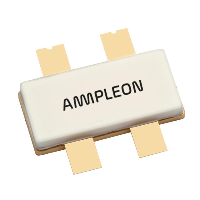
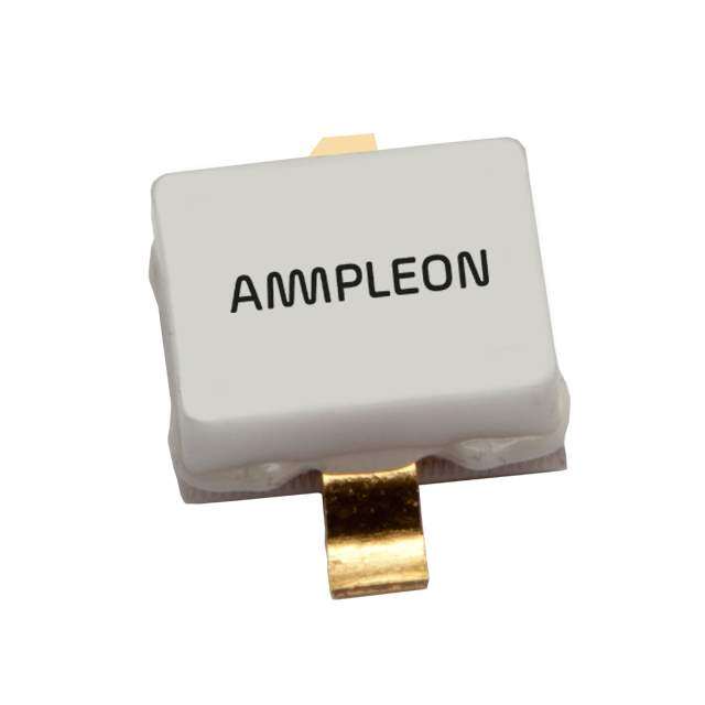
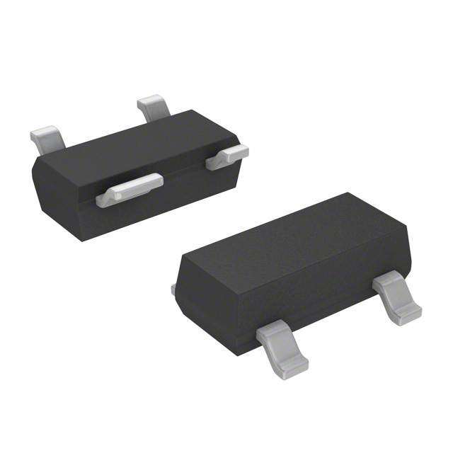
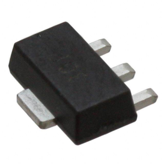
| 产品图片 |
|
| rohs | 符合RoHS无铅 / 符合限制有害物质指令(RoHS)规范要求 |
| 产品系列 | 晶体管,晶体管射频,射频JFET晶体管,CEL NE3511S02-A- |
| 数据手册 | |
| 产品型号 | NE3511S02-A |
| Pd-PowerDissipation | 165 mW |
| Pd-功率耗散 | 165 mW |
| Vds-Drain-SourceBreakdownVoltage | 4 V |
| Vds-漏源极击穿电压 | 4 V |
| Vgs-Gate-SourceBreakdownVoltage | - 3 V |
| Vgs-栅源极击穿电压 | - 3 V |
| 产品 | RF JFET |
| 产品种类 | Small Signal GaAs FETs |
| 供应商器件封装 | S02 |
| 其它名称 | NE3511S02A |
| 功率-输出 | - |
| 功率耗散 | 165 mW |
| 包装 | 散装 |
| 商标 | CEL |
| 噪声系数 | 0.3dB |
| 增益 | 13.5dB |
| 安装风格 | SMD/SMT |
| 封装/外壳 | 4-SMD,扁平引线 |
| 封装/箱体 | S0-2 |
| 技术 | GaAs |
| 晶体管极性 | N-Channel |
| 晶体管类型 | HFET |
| 最大工作温度 | + 125 C |
| 标准包装 | 1 |
| 正向跨导-最小值 | 65 mS |
| 漏极连续电流 | 70 mA |
| 漏源电压VDS | 4 V |
| 电压-测试 | 2V |
| 电压-额定 | 4V |
| 电流-测试 | 10mA |
| 类型 | GaAs HEMT |
| 闸/源击穿电压 | - 3 V |
| 闸/源截止电压 | - 0.7 V |
| 频率 | 12GHz |
| 额定电流 | 70mA |


- 商务部:美国ITC正式对集成电路等产品启动337调查
- 曝三星4nm工艺存在良率问题 高通将骁龙8 Gen1或转产台积电
- 太阳诱电将投资9.5亿元在常州建新厂生产MLCC 预计2023年完工
- 英特尔发布欧洲新工厂建设计划 深化IDM 2.0 战略
- 台积电先进制程称霸业界 有大客户加持明年业绩稳了
- 达到5530亿美元!SIA预计今年全球半导体销售额将创下新高
- 英特尔拟将自动驾驶子公司Mobileye上市 估值或超500亿美元
- 三星加码芯片和SET,合并消费电子和移动部门,撤换高东真等 CEO
- 三星电子宣布重大人事变动 还合并消费电子和移动部门
- 海关总署:前11个月进口集成电路产品价值2.52万亿元 增长14.8%


PDF Datasheet 数据手册内容提取
HETERO JUNCTION FIELD EFFECT TRANSISTOR NE3511S02 D X TO Ku BAND SUPER LOW NOISE AMPLIFIER 2 E N-CHANNEL HJ-FET K 2 U FEATURES 1 • Super low noise figure and high associated gain NF = 0.30 dB TYP., Ga = 13.5 dB TYP. @ f = 12 GHz 5 • Micro-X plastic (S02) package N 3 APPLICATIONS E • X to Ku-band DBS LNB • Other X to Ku-band communication systems C I ORDERING INFORMATION T : t Part Number Order Number Package Quantity Marking Supplying Form n NE3511S02-T1C NE3511S02-T1C-A S02 (PNb-Free) 2 kpcs/reel B •8 mm wide embossed taping e •Pin 4 (Gate) faces the perforation side NE3511S02-T1D NE3511S02-T1D-A 10 kpcs/reel of the tape m Remark To order evaluation samples, contact your nearby sales office. O Part number for sample order: NE3511S02-eA c ABSOLUTE MAXIMUM RATINGS (TA = +25°C) a Parameter C Symbol Ratings Unit l Drain to Source Voltage VDS p 4 V Gate to Source Voltage VeGS −3 V Drain Current S ID IDSS mA R Gate Current IG 100 µA Total Power Dissipation n Ptot Note 165 mW ChaInnel Temperature Tch +125 °C I Storage Temperature - Tstg −65 to +125 °C D p Note Mounted on 1.08 cm2 × 1.0 mm (t) glass epoxy PCB o r D Caution Observe precautions when handling because these devices are sensitive to electrostatic discharge. Document No. PG10642EJ01V0DS (1st edition) Date Published October 2006 NS CP(N)
NE3511S02 RECOMMENDED OPERATING CONDITIONS (TA = +25°C) D Parameter Symbol MIN. TYP. MAX. Unit Drain to Source Voltage VDS 1 2 3 V 2 E Drain Current ID 5 10 20 mA Input Power Pin − − 0 dBm K 2 ELECTRICAL CHARACTERISTICS (TA = +25°C, unless otherwiseU specified) 1 Parameter Symbol Test Conditions MIN. TYP. MAX. Unit 5 Gate to Source Leak Current IGSO V GS = −3 V − 0.5 10 µA N Saturated Drain Current IDSS V DS = 2 V, VGS = 0 V 20 340 70 mA Gate to Source Cutoff Voltage VGS (off) V DS = 2 V, ID = 100 µA −0.2 −0.7 −1.7 V E Transconductance gm V DS = 2 V, ID = 10 mA 50 65 − mS C Noise Figure NF VDS = 2 V, IDI = 10 mA, f = 12 GHz − 0.30 0.45 dB Associated Gain Ga T 12.5 13.5 − dB : t n N e m O e c a C l p e S R n I I - D p o r D 2 Data Sheet PG10642EJ01V0DS
NE3511S02 TYPICAL CHARACTERISTICS (TA = +25°C, unless otherwise specified) D TOTAL POWER DISSIPATION DRAIN CURRENT vs. vs. AMBIENT TEMPERATURE DRAIN TO SOURCE VOLTAGE 250 100 2 Mounted on Glass Epoxy PCB E W) (1.08 cm2 × 1.0 mm (t) ) P (mtot 200 mA) 80 K pation 150 nt I (D 60 U 2 Dissi 100 Curre 40 1VGS = 0 V Power Drain 5 –0.2 V al 50 N20 3 ot –0.4 V T –0.6 V E 0 50 100 150 200 250 0 1.0 2.0 Ambient Temperature TA (˚C) I DrainC to Source Voltage VDS (V) DRAIN CURRENT vs. T GATE TO SOURCE VOLTAGE : 80 t n VDS = 2N V A) 60 e m (D m nt I e 40 urr O C e n ai Dr 20 c a 0 C l –2.0 –1.0 0 p Gate to Source Voltage VGS (V) e MINIMUM NOISE FIGURE, MINIMUM NOISE FIGURE, S ASSOCIATED GAIN vs. FRREQUENCY ASSOCIATED GAIN vs. DRAIN CURRENT 2.0 25 1.6 16 dB) 1.8 n VIDD =S =1 02 mVA dB) 1.4 fV =DS 1 =2 2G VHz 14 Figure NF (minD1111I....2460 pG-aI 1250 Gain G (dB)a Figure NF (min 101...280 Ga 18120 Gain G (dB)a oise 0.8 o 10 ated oise 0.6 6 ated mum N 00..64 r NFmin 5 Associ mum N 0.4 NFmin 4 Associ ni D ni 0.2 2 Mi 0.2 Mi 0.0 0 0.0 0 0 2 4 6 8 10 12 14 16 18 20 0 5 10 15 20 25 Frequency f (GHz) Drain Current ID (mA) Remark The graphs indicate nominal characteristics. Data Sheet PG10642EJ01V0DS 3
NE3511S02 S-PARAMETERS D S-parameters/Noise parameters are provided on our web site in a form (S2P) that enables direct import to a microwave circuit simulator without keyboard input. Click here to download S-parameters. [RF and Microwave] → [Device Parameters] E 2 URL http://www.ncsd.necel.com/microwave/index.html K 2 U 1 5 N 3 E C I T : t n N e m O e c a C l p e S R n I I - D p o r D 4 Data Sheet PG10642EJ01V0DS
NE3511S02 RF MEASURING LAYOUT PATTERN (REFERENCE ONLY) (UNIT: mm) D 2.80 2.60 2 2.06 E 0.64 K 2 1.7 mm/R.P. U 1 5 N 3 E C I T 6 4 4 0 2.0 0.7 0.5 t:13. n 2.6 N Reference Plane 1.7 1.7 Reference Plane e (Calibration Plane) (Calibration Plane) m φ0.3 TH O e c L2a–uX Ver. 1 C l p 6.0 e RT/duroid 5880/ROGERS S R t = 0.254 mm εr = 2.20 n tan delta = 0.0009 @10 GHz I I - D p o r D Data Sheet PG10642EJ01V0DS 5
NE3511S02 PACKAGE DIMENSIONS D S02 (UNIT: mm) (Top View) (Bottom View) 2 E 3.2±0.2 K 0.65 TYP. 2.2±0.2 2 U 1 1 1 5 1 P. 2 0. Y B 0. ± T ±N 2.6 0.5 2 4 2.2 4 3 2 E 3 C3 I T (Side View) : t 2.2±0.2 n 1.7N e 5 AX. 0.0 m M 5± 1.5 0.1 O e 3.2±0.2 c a C l p e PIN CONNECTIONS S R 1. Source 2. Drain 3. Source n 4. Gate I I - D p o r D 6 Data Sheet PG10642EJ01V0DS
NE3511S02 RECOMMENDED SOLDERING CONDITIONS D This product should be soldered and mounted under the following recommended conditions. For soldering methods and conditions other than those recommended below, contact your nearby sales office. Soldering Method Soldering Conditions E ConditionSy2mbol Infrared Reflow Peak temperature (package surface temperature) : 260°C or below IRK260 Time at peak temperature : 10 seconds or less Time at temperature of 220°C or higher : 60 seconds or less 2 Preheating time at 120 to 180°C :U 120±30 seconds Maximum number of reflow processes : 3 times 1 Maximum chlorine content of rosin flux (% mass) : 0.2%(Wt.) or below 5 Partial Heating Peak temperature (terminal temperature) : 350°C or below HS350 Soldering time (per side of device) N: 3 seconds or less 3 Maximum chlorine content of rosin flux (% mass) : 0.2%(Wt.) or below E Caution Do not use different soldering methods together (except for partial heating). C I T : t n N e m O e c a C l p e S R n I I - D p o r D Data Sheet PG10642EJ01V0DS 7
NE3511S02 This product uses gallium arsenide (GaAs). D Caution GaAs Products GaAs vapor and powder are hazardous to human health if inhaled or ingested, so please observe the following points. •Follow related laws and ordinances when disposing of the product. If there are no applicable laws and/or ordinances, dispose of the product as recommended below. 2 E 1.Commission a disposal company able to (with a license to) collect, transport and dispose of materials that contain arsenic and other such industrial waste materials. K 2.Exclude the product from general industrial waste and household garbage, and ensure that the product is controlled (as industrial waste subject to special control) up until fina2l disposal. U •Do not burn, destroy, cut, crush, or chemically dissolve the product. 1 •Do not lick the product or in any way allow it to enter the mouth. 5 N 3 E C I T : t n N e m O e c a C l p e S R n I I - D p o r D
4590 Patrick Henry Drive Santa Clara, CA 95054-1817 D Telephone: (408) 919-2500 Facsimile: (408) 988-0279 2 E K Subject: Compliance with EU Directives 2 U 1 CEL certifies, to its knowledge, that semiconductor and laser products detailed below are compliant 5 with the requirements of European Union (EU) Directive 2002/95/EC Restriction on Use of Hazardous Substances in electrical and electronic equipment (RoHS)N and the requirements of EU Directive 3 2003/11/EC Restriction on Penta and Octa BDE. E CEL Pb-free products have the same base part number with a suffix added. The suffix –A indicates that the device is Pb-free. The –AZ suffix is used to designate devicesC containing Pb which are I exempted from the requirement of RoHS directive (*). In all ca ses the devices have Pb-free terminals. All devices with these suffixes meet the requirTements of the RoHS directive. : t This status is based on CEL’s understanding of the EU Directives and knowledge of the materials that n go into its products as of the date of disclosure of this information. N e Restricted Substance Concentration Limit per RoHS Concentration contained per RoHS (values are not yet fixmed) in CEL devices -A -AZ Lead (Pb) O < 1000 PPM Not Detected (*) e Mercury < 1000 PPM Not Detected c Cadmium < 100 PPM Not Detected a C Hexavalent Chromium <l 1000 PPM Not Detected p PBB < 1000 PPM Not Detected e PBDE < 1000 PPM Not Detected S R If you should have any additional questions regarding our devices and compliance to environmental standards, please do not hensitate to contact your local representative. I Important Information and DisclaIimer: Information provided by CEL on its website or in other communications concerting the substance content of its products represen-ts knowledge and belief as of the date that it is provided. CEL bases its knowledge and belief on information D provided by third parties and makes no representation or warranty as to the accuracy of such information. Efforts are underway to better p integrate information from third parties. CEL has taken and continues to take reasonable steps to provide representative and accurate information but may not have conducted destructive testing or chemical analysis on incoming materials and chemicals. CEL and CEL suppliers consider certaoin information to be proprietary, and thus CAS numbers and other limited information may not be available for release. In no event shall CrEL’s liability arising out of such information exceed the total purchase price of the CEL part(s) at issue sold by CEL to customer on an annual basis. See CEL TermsD and Conditions for additional clarification of warranties and liability.
NOTICE D 1. Descriptions of circuits, software and other related information in this document are provided only to illustrate the operation of semiconductor products and application examples. You are fully responsible for the incorporation of these circuits, software, and information in the design of your equipment. California Eastern Laboratories and Renesas Electronics assumes no responsibility for any losses incurred by you or third parties arising from the use of these circuits, software, or information. 2 E 2. California Eastern Laboratories has used reasonable care in preparing the information included in this document, but California Eastern Laboratories does not warrant that such information is error free. California Eastern Laboratories and Renesas Electronics assumes no liability whatsoever for any damages K incurred by you resulting from errors in or omissions from the information included herein. 3. California Eastern Laboratories and Renesas Electronics do not assume any liability for infringement of patents, copyrights, or other intellectual property rights of third parties by or arising from the use of Renesas Electronics products or technical information described in this docum2ent. No license, express, implied or otherwise, is granted hereby under any patents, copyrights or other intellectual propertyU rights of California Eastern Laboratories or Renesas Electronics or others. 1 4. You should not alter, modify, copy, or otherwise misappropriate any Renesas Electronics product, whether in whole or in part. California Eastern Laboratories and Renesas Electronics assume no responsibility for any losses incurred by you or third parties arising from such alteration, modification, copy or otherwise misappropriation of Renesas Electronics product. 5 5. Renesas Electronics products are classified according to the following two quality grades: “Standard” and “High Quality”. The recommended applications N for each Renesas Electronics product depends on the product’s quality grade, as indicated below. “Standard”: Com3puters; office equipment; communications equipment; test and measurement equipment; audio and visual equipment; home electronic appliances; machine tools; personal electronic equipment; and industrial robots etc. “High Quality”: Transportation equipment (automobiles, trains, ships, etc.); traffic control systems; anti-disaster systems; anti-crime E systems; and safety equipment etc. Renesas Electronics products are neither intended nor authorized for use in products or systems that may pose a direct threat to human life or bodily injury (artificial life support devices or systems, surgical implantations etc.), or may cause serious property damages (nuclear reactor control systems, military equipment etc.). You must check the quality grade of each Renesas EleCctronics product before using it in a particular I application. You may not use any Renesas Electronics product for any application for which it is not intended. California Eastern Laboratories and Renesas Electronics shall not be in any way liable for any damages or losses incurred by you or third parties arising from the use of any Renesas Electronics product for which the product is not intended by California Eastern LaboratoTries or Renesas Electronics. 6. You should use the Renesas Electronics products described in this document within the range s:pecified by California Eastern Laboratories, especially with respect to the maximum rating, operating supply voltage range, movement power voltage rantge, heat radiation characteristics, installation and other product characteristics. California Eastern Laboratories shall have no liability for malfunctions or damages arising out of the use of Renesas Electronics products n beyond such specified ranges. N 7. Although Renesas Electronics endeavors to improve the quality and reliability of its products, semiconductor products have specific characteristics such as the occurrence of failure at a certain rate and malfunctions under certain use conditioens. Further, Renesas Electronics products are not subject to radiation resistance design. Please be sure to implement safety measures to guard them against the possibility of physical injury, and injury or damage caused by fire in the event of the failure of a Renesas Electronics product, such as safety dmesign for hardware and software including but not limited to redundancy, fire control and malfunction prevention, appropriate treatment for aging degradation or any other appropriate measures. Because the evaluation of microcomputer software alone is very difficult, please evaluate the safety of the final products or systems manufactured by you. O 8. Please contact a California Eastern Laboratories sales office for details as to environmental matters such as the environmental compatibility of each Renesas e Electronics product. Please use Renesas Electronics products in compliance with all applicable laws and regulations that regulate the inclusion or use of controlled substances, including without limitation, the EU RoHS Directive. California Eastern Laboratories and Renesas Electronics assume no liability for c damages or losses occurring as a result of your noncompliance with applicable laws and regulations. 9. Renesas Electronics products and technology may not be used faor or incorporated into any products or systems whose manufacture, use, or sale is prohibited under any applicable domestic or foreign laws or regulations. You should not use Renesas Electronics products or technology described in this document C for any purpose relating to military applications or use by the military, including but not limited to the development of weapons of mass destruction. When l exporting the Renesas Electronics products or technology described in this document, you should comply with the applicable export control laws and p regulations and follow the procedures required by such laws and regulations. 10. It is the responsibility of the buyer or distributor of California Eastern Laboratories, who distributes, disposes of, or otherwise places the Renesas Electronics product with a third party, to notify such third partye in advance of the contents and conditions set forth in this document, California Eastern Laboratories and Renesas Electronics assume no responsibility for any losses incurred by you or third parties as a result of unauthorized use of Renesas Electronics products. S 11. This document may not be reproduced or dupliRcated in any form, in whole or in part, without prior written consent of California Eastern Laboratories. 12. Please contact a California Eastern Laboratories sales office if you have any questions regarding the information contained in this document or Renesas Electronics products, or if you have any o ther inquiries. n NOTE 1: “Renesas Electronics” as used in this document means Renesas Electronics Corporation and also includes its majority-owned subsidiaries. NOTE 2: “RIenesas Electronics product(s)” means any product developed or manufactured by or for Renesas Electronics. I NOTE 3: Products and product information are subject to change without notice. - D p CEL Heaodquarters • 4590 Patrick Henry Drive, Santa Clara, CA 95054 • Phone (408) 919-2500 • www.cel.com For a complete list of sales offices, representatives and distributors, r Please visit our website: www.cel.com/contactus D