ICGOO在线商城 > 分立半导体产品 > 晶体管 - FET,MOSFET - 单 > NDT3055L
/NDT3055L.jpg)
 Datasheet下载
- 型号: NDT3055L
- 制造商: Fairchild Semiconductor
- 库位|库存: xxxx|xxxx
- 要求:
| 数量阶梯 | 香港交货 | 国内含税 |
| +xxxx | $xxxx | ¥xxxx |
查看当月历史价格
查看今年历史价格
NDT3055L产品简介:
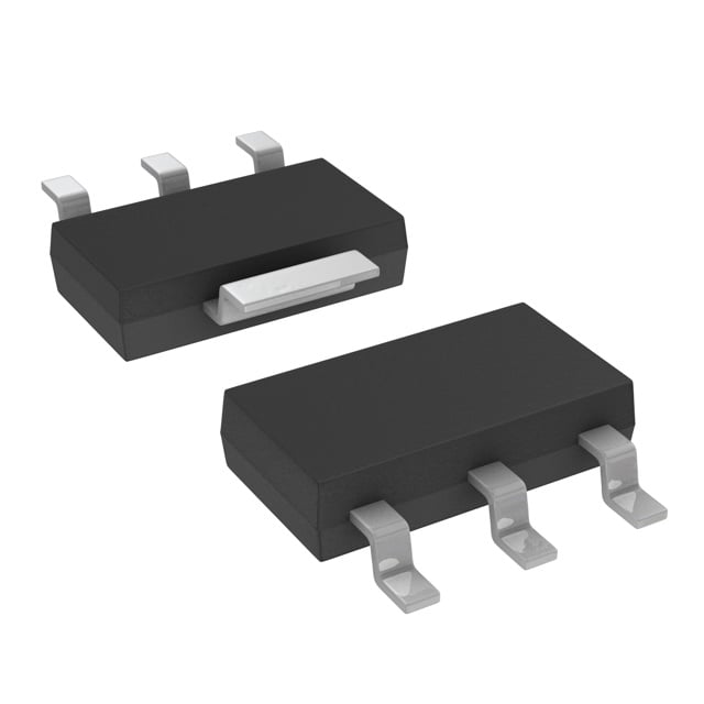
ICGOO电子元器件商城为您提供NDT3055L由Fairchild Semiconductor设计生产,在icgoo商城现货销售,并且可以通过原厂、代理商等渠道进行代购。 NDT3055L价格参考。Fairchild SemiconductorNDT3055L封装/规格:晶体管 - FET,MOSFET - 单, N-Channel 60V 4A (Ta) 3W (Ta) Surface Mount SOT-223-4。您可以下载NDT3055L参考资料、Datasheet数据手册功能说明书,资料中有NDT3055L 详细功能的应用电路图电压和使用方法及教程。
| 参数 | 数值 |
| 产品目录 | |
| ChannelMode | Enhancement |
| 描述 | MOSFET N-CH 60V 4A SOT-223-4MOSFET SOT-223 N-CH LOGIC |
| 产品分类 | FET - 单分离式半导体 |
| FET功能 | 逻辑电平门 |
| FET类型 | MOSFET N 通道,金属氧化物 |
| Id-ContinuousDrainCurrent | 4 A |
| Id-连续漏极电流 | 4 A |
| 品牌 | Fairchild Semiconductor |
| 产品手册 | |
| 产品图片 |
|
| rohs | RoHS 合规性豁免无铅 / 符合限制有害物质指令(RoHS)规范要求 |
| 产品系列 | 晶体管,MOSFET,Fairchild Semiconductor NDT3055L- |
| 数据手册 | |
| 产品型号 | NDT3055L |
| Pd-PowerDissipation | 3 W |
| Pd-功率耗散 | 3 W |
| RdsOn-Drain-SourceResistance | 70 mOhms |
| RdsOn-漏源导通电阻 | 70 mOhms |
| Vds-Drain-SourceBreakdownVoltage | 60 V |
| Vds-漏源极击穿电压 | 60 V |
| Vgs-Gate-SourceBreakdownVoltage | +/- 20 V |
| Vgs-栅源极击穿电压 | 20 V |
| 上升时间 | 7.5 ns |
| 下降时间 | 7 ns |
| 不同Id时的Vgs(th)(最大值) | 2V @ 250µA |
| 不同Vds时的输入电容(Ciss) | 345pF @ 25V |
| 不同Vgs时的栅极电荷(Qg) | 20nC @ 10V |
| 不同 Id、Vgs时的 RdsOn(最大值) | 100 毫欧 @ 4A,10V |
| 产品培训模块 | http://www.digikey.cn/PTM/IndividualPTM.page?site=cn&lang=zhs&ptm=356http://www.digikey.cn/PTM/IndividualPTM.page?site=cn&lang=zhs&ptm=6736 |
| 产品目录页面 | |
| 产品种类 | MOSFET |
| 供应商器件封装 | SOT-223-3 |
| 其它名称 | NDT3055LCT |
| 典型关闭延迟时间 | 20 ns |
| 功率-最大值 | 1.1W |
| 包装 | 剪切带 (CT) |
| 单位重量 | 188 mg |
| 商标 | Fairchild Semiconductor |
| 安装类型 | 表面贴装 |
| 安装风格 | SMD/SMT |
| 封装 | Reel |
| 封装/外壳 | TO-261-4,TO-261AA |
| 封装/箱体 | SOT-223-3 |
| 工厂包装数量 | 4000 |
| 晶体管极性 | N-Channel |
| 最大工作温度 | + 150 C |
| 最小工作温度 | - 65 C |
| 标准包装 | 1 |
| 正向跨导-最小值 | 7 S |
| 漏源极电压(Vdss) | 60V |
| 电流-连续漏极(Id)(25°C时) | 4A (Ta) |
| 系列 | NDT3055 |
| 通道模式 | Enhancement |
| 配置 | Single |
| 零件号别名 | NDT3055L_NL |


.jpg)


- 商务部:美国ITC正式对集成电路等产品启动337调查
- 曝三星4nm工艺存在良率问题 高通将骁龙8 Gen1或转产台积电
- 太阳诱电将投资9.5亿元在常州建新厂生产MLCC 预计2023年完工
- 英特尔发布欧洲新工厂建设计划 深化IDM 2.0 战略
- 台积电先进制程称霸业界 有大客户加持明年业绩稳了
- 达到5530亿美元!SIA预计今年全球半导体销售额将创下新高
- 英特尔拟将自动驾驶子公司Mobileye上市 估值或超500亿美元
- 三星加码芯片和SET,合并消费电子和移动部门,撤换高东真等 CEO
- 三星电子宣布重大人事变动 还合并消费电子和移动部门
- 海关总署:前11个月进口集成电路产品价值2.52万亿元 增长14.8%


PDF Datasheet 数据手册内容提取
Is Now Part of To learn more about ON Semiconductor, please visit our website at www.onsemi.com Please note: As part of the Fairchild Semiconductor integration, some of the Fairchild orderable part numbers will need to change in order to meet ON Semiconductor’s system requirements. Since the ON Semiconductor product management systems do not have the ability to manage part nomenclature that utilizes an underscore (_), the underscore (_) in the Fairchild part numbers will be changed to a dash (-). This document may contain device numbers with an underscore (_). Please check the ON Semiconductor website to verify the updated device numbers. The most current and up-to-date ordering information can be found at www.onsemi.com. Please email any questions regarding the system integration to Fairchild_questions@onsemi.com. ON Semiconductor and the ON Semiconductor logo are trademarks of Semiconductor Components Industries, LLC dba ON Semiconductor or its subsidiaries in the United States and/or other countries. ON Semiconductor owns the rights to a number of patents, trademarks, copyrights, trade secrets, and other intellectual property. A listing of ON Semiconductor’s product/patent coverage may be accessed at www.onsemi.com/site/pdf/Patent-Marking.pdf. ON Semiconductor reserves the right to make changes without further notice to any products herein. ON Semiconductor makes no warranty, representation or guarantee regarding the suitability of its products for any particular purpose, nor does ON Semiconductor assume any liability arising out of the application or use of any product or circuit, and specifically disclaims any and all liability, including without limitation special, consequential or incidental damages. Buyer is responsible for its products and applications using ON Semiconductor products, including compliance with all laws, regulations and safety requirements or standards, regardless of any support or applications information provided by ON Semiconductor. “Typical” parameters which may be provided in ON Semiconductor data sheets and/or specifications can and do vary in different applications and actual performance may vary over time. All operating parameters, including “Typicals” must be validated for each customer application by customer’s technical experts. ON Semiconductor does not convey any license under its patent rights nor the rights of others. ON Semiconductor products are not designed, intended, or authorized for use as a critical component in life support systems or any FDA Class 3 medical devices or medical devices with a same or similar classification in a foreign jurisdiction or any devices intended for implantation in the human body. Should Buyer purchase or use ON Semiconductor products for any such unintended or unauthorized application, Buyer shall indemnify and hold ON Semiconductor and its officers, employees, subsidiaries, affiliates, and distributors harmless against all claims, costs, damages, and expenses, and reasonable attorney fees arising out of, directly or indirectly, any claim of personal injury or death associated with such unintended or unauthorized use, even if such claim alleges that ON Semiconductor was negligent regarding the design or manufacture of the part. ON Semiconductor is an Equal Opportunity/Affirmative Action Employer. This literature is subject to all applicable copyright laws and is not for resale in any manner.
Aug us t 1998 N L5503TD N lennahC- tcnie gmleoeedLc rvondoeM altLthescniieEFsfnfaErT noitpircs e lDareneG serutaeF esehT tn ec mile egedlconoenlrnmvaeaehwhlnoCep-N 4 A 6 , R .V 0 001.0 = W @V 01 = ,V dleif tceffe srotsisnart era decudorp gnisudlihcriaF 's R NO(SD 021.0 = ) W @V GS 5.4 = V . ,yrateirporp hgih llec ,ytisned SOMD .ygolonhcetsihT NO(SD ) GS yrev hgih ytisned ssecorp si yllaicepse deroliat ot cigol morf yltcerid noitarepo gniwolla stnemeriuqer evird woL eziminim etats-no ecnatsiser dna edivorp roirepus V .srevird .V2 < )HT(SG eys gldhrungepain the, sedhcntnaiawmr ogfnriehpctiws sedom noitatummoc dna ehcnalava eht ni . secived esehT ngised llec ytisned hgiH R wol ylemertxe rof )NO(SD . sa hcus snoitacilppa egatlov wol rof detius ylralucitrap era desu ylediw a ni ytilibapac gnildnah tnerruc dna rewop hgiH CD rotomlortnoc dna CD/CD noisrevnoc erehwtsaf .egakcap tnuom ecafrus ,gnihctiws wol enil-ni rewop ,ssol dna ecnatsiserot .dedeen era stneisnart SuperSOT MT -3 SuperSOT TM -6 SuperSOT TM -8 8-OS SOT-223 SOIC-16 D D D D S S D G G D S SOT-223 * G G S SOT-223 (J23Z) sgnitaR mumixaM etulosbA T 52 = deton esiwrehto soselnu C A lobmyS retemaraP N L5503TD stinU V egatloV ecruoS-niarD 06 V SSD V egatloV ecruoS-etaG suoun itnoC - ± 02 V SSG ID suounitnoC - tnerruC niarD mumixaM )a1 etoN( 4 A desluP - 52 P D mumixaM noitapissiD rewoP a1 etoN( ) 3 W 1 etoN( )b 3.1 c1 etoN( ) 1.1 T T, egnaR erutarepmeT egarotS dna gnitarepO 051 ot 56- C° J GTS SCITSIRETCARAHC LAMREHT R qAJ tneibmA-ot-noitcnuJ ,ecnatsiseR lamrehT )a1 etoN( 24 W/C° R qCJ esaC-ot-noitcnuJ ,ecnatsiseR lamrehT )1 etoN( 21 W/C° .dael niard retnec depporc rof Z32J noitpo redrO * © 1998 Fairchild Semiconductor Corporation NDT3055L Rev.A1
scitsiretcarahC lacirtcelE (T = 25 OC unless otherwise noted ) A lobmyS retemaraP snoitidnoC niM pyT xaM stinU SCITSIRETCARAHC FFO VB egatloV nwodkaerB ecruoS-niarD V I ,V 0 = Aµ 052 = 06 V SSD SG D D VB /D T tneiciffeoC .pmeT egatloV nwodkaerB I =Aµ 052 52 ot decnerefeR , o C 55 /Vm o C SSD J D I tnerruC niarD egatloV etaG oreZ V = 06 ,V V V 0 = 1 µ A SSD SD SG T 21= C°5 05 µ A J I drawroF ,egakaeL ydoB - etaG V = 02 V ,V V 0 = 001 An FSSG SG SD I esreveR ,egakaeL ydoB - etaG V - = 02 V ,V V 0 = 001- An RSSG SG SD SCITSIRETCARAHC NO 2 etoN( ) V egatloV dlohserhT etaG V V = , I Aµ 052 = 1 6.1 2 V SG )ht( SD SG D D V /D T egatloV dlohserhT etaG tneiciffeoC .pmeT I = Aµ 052 52 ot decnerefeR , oC 4- / Vm oC )ht(SG J D R ecnatsiseR-nO ecruoS-niarD citatS V 01 = ,V I 4 = A 70.0 1.0 W )NO(SD SG D T 21= C°5 521.0 81.0 J V 5.4 = ,V I 7.3 = A 301.0 21.0 SG D I tnerruC niarD etatS-nO V 5 = V , 01 = V 01 A )NO(D SG SD g ecnatcudnocsnarT drawroF V 5 = I ,V 4 = A 7 S SF SD D CIMANYD SCITSIRETCARAHC C ecnaticapaC tupnI V 52 = V , ,V 0 = 543 Fp ssi SD SG zHM 0.1 = f C ecnaticapaC tuptuO 011 Fp sso C ecnaticapaC refsnarT esreveR 03 Fp ssr HC GNIHCTIWS SCITSIRETCARA 2 etoN( ) t emiT yaleD nO - nruT V 52 = I , 1 = ,A 5 02 sn no(D ) DD D t emiT esiR nO - nruT V SG 01 = R ,V NEG 6 = W 5.7 02 sn r t emiT yaleD ffO - nruT 02 05 sn )ffo(D t emiT llaF ffO - nruT 7 02 sn f Q egrahC etaG latoT V V 04 = I , 4 = ,A 31 02 Cn g SD D V 01 = V Q egrahC ecruoS-etaG SG 7.1 Cn sg Q egrahC niarD-etaG 2.3 Cn dg SGNITAR MUMIXAM DNA SCITSIRETCARAHC EDOID ECRUOS-NIARD I tnerruC drawroF edoiD ecruoS-niarD suounitnoC mumixaM 5.2 A S V DS egatloV drawroF edoiD ecruoS-niarD V SG I ,V 0 = S5.2 = A 2 e toN( ) 8.0 2.1 V Notes: 1. R d ese nahe it csfnieedsr elfaemr r eeeesh rhateetcchnwats ilsaemr rtenhetibma-ot- eedssnaaacc-ot-no i tsem cihufentsohutj e cfa ofgr nuist n rueodml o . s n nieiahprtd R is qAJ qJC deetnaraug R elihw ngised yb .ngised draob s'resu eht yb denimreted si qAC .a24 o dneotn uno emWh/wC a 1 ni 2 pad of b59 . o no detnuom nehw W/C 660.0 a ni 2 .c 011 o no detnuom nehw W/C 32100.0 a uC zo2 . C2uoopzfa d . ni 2C2uoopzfa d . repap ezis rettel no 1 : 1 elacS .2 htdiW esluP :tseT esluP <µ003 elcyC ytuD ,s < %0.2 NDT3055L Rev.A1
scitsiret claarcaih rCltacceilpEyT 52 2 V =10V SG 6.0V 02 5.0V 8.1 V = 4.0V SG 4.5V 6.1 51 V5. 4 4. 0V 4.1 V0. 5 01 V0. 6 3.5V 2.1 V0. 8 V0 1 5 DS(ON) 3.0V R , NORMALIZED 1 I , DRAIN-SOURCE CURRENT (A)D DRAIN-SOURCE ON-RESISTANCE 0 8.0 0 1 2 3 4 5 0 5 01 51 02 52 (DVR)AVIONL-TSAOGUE,R CE V SD )A( TNERRUC NIARD , ID Figure 1. On-Region Characteristics . Figure 2. On-Resistance Variation with niarD tnerruC dna etaGegatloV . 8.1 0.28 I = 4.0 AD 0.24 I =A2D 6.1 V = 10 V GS 0.2 4.1 0.16 2.1 CT °5 2=1 A 0.12 1 0.08 DS(ON) C °52 R , NORMALIZED 8.0 0.04 DS(ON) DRAIN-SOURCE ON-RESISTANCE6.0 05- 52- 0 52 05 57 001 521 051 R , ON-RESISTANCE (OHM) 0 2 4 6 8 10 )C°( ERUTAREPMET NOITCNUJ , T J V, G ATET OS OURCEV OLTAGE( V)SG Figure 3. On-Resistance Variation erugiF4 . ecnatsiseR-nO Variation with with Temperature . Gate-to - ecruoS.egatloV 01 03 V = 5V DS T =C°55-J 25°C 01 V = 0V SG 8 125°C 1 T= 1 25°CA 6 1.0 25°C -55 °C 4 10.0 I , DRAIN CURRENT (A)D 2 100.0 I , REVERSE DRAIN CURRENT (A)S 0 1000.0 1 5.1 2 5.2 3 5.3 4 5.4 5 0 2.0 4.0 6.0 8.0 1 2.1 4.1 )V( EGATLOV ECRUOS OT ETAG , V GS )V( EGATLOV DRAWROF EDOID YDOB , V SD erugiF 5 . Transfer Characteristics. erugiF6 ega tdlro aV w.er do yoFdioDB noitairaV htiw tnerruC dna Temperature. NDT3055L Rev.A1
Typical Electrical scitsiretcarahC (continued) 0001 01 I A=4D V = 10V SD 005 8 V03 C ssi V04 002 6 C sso 001 4 05 C ssr 2 CAPACITANCE (pF) zHM 1 = f 02 V 0 =V SG V , GATE-SOURCE VOLTAGE (V)GS 0 01 0 2 4 6 8 01 21 41 1.0 3.0 1 4 01 03 06 )Cn( EGRAHC ETAG , Q g )V( EGATLOV ECRUOS OT NIARD , V SD erugiF7 . Gate Charge Characteristics. Figure 8. ecnaticapaCscitsiretcarahC . 05 08 100us SINGLE PULSE 01 TIM I)LNO(SDR 1ms 06 R =110°C/W qAJ 3 10ms T C °=52 A 1 100ms 1s 04 0.3 10s DC 0.1 V = 10V GS POWER (W) SINGLE PULSE 02 I , DRAIN CURRENT (A)D30.0 R = 110 C/W qAJ o T = 25°C A 10.0 0 1.0 0.2 0.5 1 2 5 01 03 06 001 100.0 10.0 1.0 1 01 001 003 )V( EGATLOV ECRUOS-NIARD , V DS )CES( EMIT ESLUP ELGNIS Figure 9. Maximum Safe Operating Area. erugiF01 . Single Pulse Maximum Power Dissipation. 1 5.0 D=0 .5 2.0 0 . 2 1.0 0 .1 R (t) = r(t) * R qJA qAJ 50.0 0.0 5 = R1 10° C/W qAJ 20.0 0.0 2 P(pk) 10.0 0.0 1 500.0 t 1 t 2 r(t), NORMALIZED EFFECTIVE 200.0 Si nglPeu lse T- T = P * R ( t)J A qAJ Duty Cycle, D = t / t TRANSIENT THERMAL RESISTANCE 100.0 1 2 1000.0 100.0 10.0 1.0 1 01 001 003 )ces( EMIT , t1 erugiF11 . tneisnarT lamrehT esnopseRevruC . c1 eton ni debircsed snoitidnoc eht gnisu demrofrep noitaziretcarahc lamrehT . lamreht tneisnarT .ngised draob tiucric eht no gnidneped egnahc lliw esnopser NDT3055L Rev.A1
6.70 B 6.20 0.10 C B 3.10 2.90 3.25 4 1.90 A 3.70 6.10 3.30 1.90 1 3 0.84 0.60 2.30 0.95 2.30 4.60 0.10 C B LAND PATTERN RECOMMENDATION SEE DETAIL A 1.80 MAX 0.08 C 7.30 C 0.10 6.70 0.00 NOTES: UNLESS OTHERWISE SPECIFIED A) DRAWING BASED ON JEDEC REGISTRATION TO-261C, VARIATION AA. B) ALL DIMENSIONS ARE IN MILLIMETERS. R0.15±0.05 10° C) DIMENSIONS DO NOT INCLUDE BURRS GAGE 5° OR MOLD FLASH. MOLD FLASH OR BURRS R0.15±0.05 DOES NOT EXCEED 0.10MM. PLANE D) DIMENSIONING AND TOLERANCING PER ASME Y14.5M-2009. 0.35 10° E) LANDPATTERN NAME: SOT230P700X180-4BN 0° TYP 0.20 F) DRAWING FILENAME: MKT-MA04AREV3 0.25 10° 5° 0.60 MIN SEATING 1.70 PLANE DETAIL A SCALE: 2:1
ON Semiconductor and are trademarks of Semiconductor Components Industries, LLC dba ON Semiconductor or its subsidiaries in the United States and/or other countries. ON Semiconductor owns the rights to a number of patents, trademarks, copyrights, trade secrets, and other intellectual property. A listing of ON Semiconductor’s product/patent coverage may be accessed at www.onsemi.com/site/pdf/Patent−Marking.pdf. ON Semiconductor reserves the right to make changes without further notice to any products herein. ON Semiconductor makes no warranty, representation or guarantee regarding the suitability of its products for any particular purpose, nor does ON Semiconductor assume any liability arising out of the application or use of any product or circuit, and specifically disclaims any and all liability, including without limitation special, consequential or incidental damages. Buyer is responsible for its products and applications using ON Semiconductor products, including compliance with all laws, regulations and safety requirements or standards, regardless of any support or applications information provided by ON Semiconductor. “Typical” parameters which may be provided in ON Semiconductor data sheets and/or specifications can and do vary in different applications and actual performance may vary over time. All operating parameters, including “Typicals” must be validated for each customer application by customer’s technical experts. ON Semiconductor does not convey any license under its patent rights nor the rights of others. ON Semiconductor products are not designed, intended, or authorized for use as a critical component in life support systems or any FDA Class 3 medical devices or medical devices with a same or similar classification in a foreign jurisdiction or any devices intended for implantation in the human body. Should Buyer purchase or use ON Semiconductor products for any such unintended or unauthorized application, Buyer shall indemnify and hold ON Semiconductor and its officers, employees, subsidiaries, affiliates, and distributors harmless against all claims, costs, damages, and expenses, and reasonable attorney fees arising out of, directly or indirectly, any claim of personal injury or death associated with such unintended or unauthorized use, even if such claim alleges that ON Semiconductor was negligent regarding the design or manufacture of the part. ON Semiconductor is an Equal Opportunity/Affirmative Action Employer. This literature is subject to all applicable copyright laws and is not for resale in any manner. PUBLICATION ORDERING INFORMATION LITERATURE FULFILLMENT: N. American Technical Support: 800−282−9855 Toll Free ON Semiconductor Website: www.onsemi.com Literature Distribution Center for ON Semiconductor USA/Canada 19521 E. 32nd Pkwy, Aurora, Colorado 80011 USA Europe, Middle East and Africa Technical Support: Order Literature: http://www.onsemi.com/orderlit Phone: 303−675−2175 or 800−344−3860 Toll Free USA/Canada Phone: 421 33 790 2910 Fax: 303−675−2176 or 800−344−3867 Toll Free USA/Canada Japan Customer Focus Center For additional information, please contact your local Email: orderlit@onsemi.com Phone: 81−3−5817−1050 Sales Representative © Semiconductor Components Industries, LLC www.onsemi.com www.onsemi.com 1
Mouser Electronics Authorized Distributor Click to View Pricing, Inventory, Delivery & Lifecycle Information: O N Semiconductor: NDT3055L