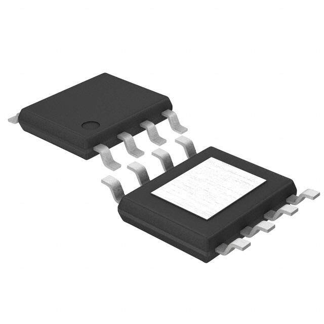
ICGOO在线商城 > 集成电路(IC) > PMIC - 稳压器 - 线性 > NCV87706DT50RKG
- 型号: NCV87706DT50RKG
- 制造商: ON Semiconductor
- 库位|库存: xxxx|xxxx
- 要求:
| 数量阶梯 | 香港交货 | 国内含税 |
| +xxxx | $xxxx | ¥xxxx |
查看当月历史价格
查看今年历史价格
NCV87706DT50RKG产品简介:
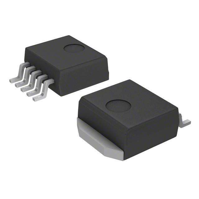
ICGOO电子元器件商城为您提供NCV87706DT50RKG由ON Semiconductor设计生产,在icgoo商城现货销售,并且可以通过原厂、代理商等渠道进行代购。 NCV87706DT50RKG价格参考¥询价-¥询价。ON SemiconductorNCV87706DT50RKG封装/规格:PMIC - 稳压器 - 线性, Linear Voltage Regulator IC Positive Fixed 1 Output 5V 350mA DPAK-5。您可以下载NCV87706DT50RKG参考资料、Datasheet数据手册功能说明书,资料中有NCV87706DT50RKG 详细功能的应用电路图电压和使用方法及教程。
| 参数 | 数值 |
| 产品目录 | 集成电路 (IC)半导体 |
| 描述 | IC REG LDO 5V 0.35A低压差稳压器 350 MA LDO |
| 产品分类 | |
| 品牌 | ON Semiconductor |
| 产品手册 | |
| 产品图片 | |
| rohs | 符合RoHS无铅 / 符合限制有害物质指令(RoHS)规范要求 |
| 产品系列 | 电源管理 IC,低压差稳压器,ON Semiconductor NCV87706DT50RKG- |
| mouser_ship_limit | 该产品可能需要其他文件才能进口到中国。 |
| 数据手册 | |
| 产品型号 | NCV87706DT50RKG |
| PSRR/纹波抑制—典型值 | 54 dB |
| 产品 | LDO Regulator |
| 产品种类 | 低压差稳压器 |
| 供应商器件封装 | DPAK-5 |
| 其它名称 | NCV87706DT50RKGOSDKR |
| 包装 | Digi-Reel® |
| 商标 | ON Semiconductor |
| 回动电压—最大值 | 875 mV |
| 安装类型 | 表面贴装 |
| 安装风格 | SMD/SMT |
| 封装 | Reel |
| 封装/外壳 | TO-252-5,DPak(4 引线 + 接片),TO-252AD |
| 封装/箱体 | DPAK-5 |
| 工作温度 | -40°C ~ 150°C |
| 工厂包装数量 | 2500 |
| 最大工作温度 | + 150 C |
| 最大输入电压 | 40 V |
| 最小工作温度 | - 40 C |
| 最小输入电压 | 5.5 V |
| 标准包装 | 1 |
| 电压-跌落(典型值) | 0.44V @ 350mA |
| 电压-输入 | 5.5 V ~ 40 V |
| 电压-输出 | 5V |
| 电压调节准确度 | 1.5 % |
| 电流-输出 | 350mA |
| 电流-限制(最小值) | 400mA |
| 稳压器拓扑 | 正,固定式 |
| 稳压器数 | 1 |
| 类型 | Ultra-Low Quiescent Current |
| 系列 | NCV8770 |
| 线路调整率 | 20 mV |
| 负载调节 | 35 mV |
| 输出电压 | 5 V |
| 输出电流 | 350 mA |
| 输出端数量 | 1 Output |
| 输出类型 | Fixed |



PDF Datasheet 数据手册内容提取
NCV8770 LDO Regulator - Ultra Low I Reset q, 350 mA The NCV8770 is 350 mA LDO regulator with integrated reset functions dedicated for microprocessor applications. Its robustness allows http://onsemi.com NCV8770 to be used in severe automotive environments. Ultra low quiescent current as low as 21 (cid:2)A typical makes it suitable for MARKING applications permanently connected to battery requiring ultra low DIAGRAMS quiescent current with or without load. This feature is especially critical when modules remain in active mode when ignition is off. The NCV8770 contains protection functions as current limit, thermal shutdown and DPAK−5 770yxxG DT SUFFIX ALYWW reverse output current protection. CASE 175AA Features • Output Voltage Options: 5 V • Output Voltage Accuracy: ±1.5% (T = 25°C to 125°C) J • Output Current up to 350 mA • Ultra Low Quiescent Current: typ 21 (cid:2)A (max 28 (cid:2)A) D2PAK−5 NC • Very Wide Range of C and ESR Values for Stability D5S SUFFIX V8770yxx • out CASE 936A AWLYWWG Microprocessor Compatible Control Functions: − Reset with Adjustable Power−On Delay • Wide Input Voltage Operation Range: up to 40 V • Protection Features y = Timing and Reset Threshold Option − Current Limitation xx = Voltage Option − Thermal Shutdown A = Assembly Location • WL, L = Wafer Lot These are Pb−Free Devices Y = Year WW = Work Week Typical Applications G or (cid:2) = Pb−Free Package • Body Control Module • Instruments and Clusters • Occupant Protection and Comfort • ORDERING INFORMATION Powertrain See detailed ordering and shipping information in the package dimensions section on page 11 of this data sheet. VBAT Vout Vin Vout VDD Cin Cout 0.1 (cid:2)F NCV8770 1 (cid:2)F Microprocessor DT RO RESET GND Figure 1. Typical Application Schematic © Semiconductor Components Industries, LLC, 2013 1 Publication Order Number: September, 2019 − Rev. 1 NCV8770/D
NCV8770 Vin Vout Thermal Shutdown RO Driver With Current Erorr Amplifier Reset Comparator Reset Driver Limit Reference Timing DT Circuit * Timer GND * Pull−Down Resistor (typ 150 k(cid:3)) active only in Reset State Figure 2. Simplified Block Diagram PIN CONNECTIONS PIN 1.Vin PIN 1.Vin 2.RO 2.RO Tab, 3.GND Tab, 3.GND 4.DT 4.DT 5.Vout 5.Vout 1 1 DPAK−5 D2PAK−5 Figure 3. Pin Connections PIN FUNCTION DESCRIPTION Pin No. DPAK−5 D2PAK−5 Pin Name Description 1 Vin Positive Power Supply Input. Connect 0.1 (cid:2)F capacitor to ground. 2 RO Reset Output. 30 k(cid:3) internal Pull−up resistor connected to Vout. RO goes Low when Vout drops by more than 7% (typ) from its nominal value (for NCV8770y devices with y = 1,2,3,...) or more than 10% (typ) from its nominal value (for NCV8770y devices with y = A, B, C,...). 3, TAB GND Power Supply Ground. 4 DT Reset Delay Time Select. Short to GND or connected to Vout to select time. 5 Vout Regulated Output Voltage. Connect 1 (cid:2)F capacitor with ESR < 100 (cid:3) to ground. − NC Not Connected − GND Exposed Pad is Connected to Ground. http://onsemi.com 2
NCV8770 ABSOLUTE MAXIMUM RATINGS Rating Symbol Min Max Unit Input Voltage (Note 1) DC Vin −0.3 40 V Transient, t < 100 ms − 45 Input Current Iin −5 − mA Output Voltage (Note 2) Vout −0.3 5.5 V Output Current Iout −3 Current Limited mA DT (Reset Delay Time Select) Voltage VDT −0.3 5.5 V DT (Reset Delay Time Select) Current IDT −1 1 mA Reset Output Voltage VRO −0.3 5.5 V Reset Output Current IRO −3 3 mA Junction Temperature TJ −40 150 °C Storage Temperature TSTG −55 150 °C Stresses exceeding Maximum Ratings may damage the device. Maximum Ratings are stress ratings only. Functional operation above the Recommended Operating Conditions is not implied. Extended exposure to stresses above the Recommended Operating Conditions may affect device reliability. 1. Refer to ELECTRICAL CHARACTERISTICS and APPLICATION INFORMATION for Safe Operating Area. 2. 5.5 V or (Vin + 0.3 V) (whichever is lower). ESD CAPABILITY (Note 3) Rating Symbol Min Max Unit ESD Capability, Human Body Model ESDHBM −2 2 kV ESD Capability, Machine Model ESDMM −200 200 V ESD Capability, Charged Device Model ESDCDM −1 1 kV 3. This device series incorporates ESD protection and is tested by the following methods: ESD Human Body Model tested per AEC−Q100−002 (JS−001−2010) ESD Machine Model tested per AEC−Q100−003 (EIA/JESD22−A115) ESD Charge Device Model tested per AEC−Q100−011 (EIA/JESD22−C101) LEAD SOLDERING TEMPERATURE AND MSL (Note 4) Rating Symbol Min Max Unit Moisture Sensitivity Level DPAK−5 MSL 1 − D2PAK−5 1 Lead Temperature Soldering TSLD °C Reflow (SMD Styles Only), Pb−Free Versions − 265 peak 4. For more information, please refer to our Soldering and Mounting Techniques Reference Manual, SOLDERRM/D. THERMAL CHARACTERISTICS (Note 5) Rating Symbol Value Unit Thermal Characteristics, DPAK−5 °C/W Thermal Resistance, Junction−to−Air (Note 6) R(cid:4)JA 56 Thermal Reference, Junction−to−Case (Note 6) R(cid:5)JC 8.4 Thermal Characteristics, D2PAK−5 °C/W Thermal Resistance, Junction−to−Air (Note 6) R(cid:4)JA 53 Thermal Reference, Junction−to−Case (Note 6) R(cid:5)JC 8.4 5. Refer to ELECTRICAL CHARACTERISTICS and APPLICATION INFORMATION for Safe Operating Area. 6. Values based on copper area of 645 mm2 (or 1 in2) of 1 oz copper thickness and FR4 PCB substrate. RECOMMENDED OPERATING RANGE (Note 7) Rating Symbol Min Max Unit Input Voltage (Note 8) Vin 5.5 40 V Junction Temperature TJ −40 150 °C 7. Refer to ELECTRICAL CHARACTERISTICS and APPLICATION INFORMATION for Safe Operating Area. 8. Minimum Vin = 5.5 V or (Vout + VDO), whichever is higher. http://onsemi.com 3
NCV8770 ELECTRICAL CHARACTERISTICS Vin = 13.2 V, Cin = 0.1 (cid:2)F, Cout = 1 (cid:2)F, for typical values TJ = 25°C, for min/max values TJ = −40°C to 150°C; unless otherwise noted. (Notes 9 and 10) Parameter Test Conditions Symbol Min Typ Max Unit REGULATOR OUTPUT Output Voltage (Accuracy %) TJ = 25 °C to 125 °C Vout V Vin = 5.575 V to 16 V, Iout = 0.1 mA to 200 mA 4.925 5.0 5.075 (−1.5 %) (+1.5%) Output Voltage (Accuracy %) Vout V Vin = 5.6 V to 40 V, Iout = 0.1 mA to 200 mA 4.9 5.0 5.1 Vin = 5.975 V to 16 V, Iout = 0.1 mA to 350 mA 4.9 5.0 5.1 (−2 %) (+2%) Output Voltage (Accuracy %) TJ = −40°C to 125°C Vout V Vin = 5.975 V to 28 V, Iout = 0 mA to 350 mA 4.9 5.0 5.1 (−2 %) (+2%) Line Regulation Vin = 6 V to 28 V, Iout = 5 mA Regline −20 0 20 mV Load Regulation Iout = 0.1 mA to 350 mA Regload −35 0 35 mV Dropout Voltage (Note 11) VDO mV Iout = 200 mA − 250 500 Iout = 350 mA − 440 875 QUIESCENT CURRENT Quiescent Current (Iq = Iin − Iout) Iq (cid:2)A Iout = 0.1 mA, TJ = 25°C − 21 27 Iout = 0.1 mA to 350 mA, TJ ≤ 125°C − − 28 CURRENT LIMIT PROTECTION Current Limit Vout = 0.96 x Vout_nom ILIM 400 − 1100 mA Short Circuit Current Limit Vout = 0 V ISC 400 − 1100 mA PSRR Power Supply Ripple Rejection (Note 12) f = 100 Hz, 0.5 Vpp PSRR − 54 − dB DT (RESET DELAY TIME SELECT) DT Threshold Voltage Vth(DT) V Logic Low − − 0.8 Logic High 2.0 − − DT Input Current VDT = 5 V IDT − − 1.0 (cid:2)A 9. Refer to ABSOLUTE MAXIMUM RATINGS and APPLICATION INFORMATION for Safe Operating Area. 10.Performance guaranteed over the indicated operating temperature range by design and/or characterization tested at TA (cid:2) TJ. Low duty cycle pulse techniques are used during testing to maintain the junction temperature as close to ambient as possible. 11.Measured when output voltage falls 100 mV below the regulated voltage at Vin = 13.2 V. 12.Values based on design and/or characterization. 13.See APPLICATION INFORMATION section for Reset Thresholds and Reset Delay Time Options http://onsemi.com 4
NCV8770 ELECTRICAL CHARACTERISTICS Vin = 13.2 V, Cin = 0.1 (cid:2)F, Cout = 1 (cid:2)F, for typical values TJ = 25°C, for min/max values TJ = −40°C to 150°C; unless otherwise noted. (Notes 9 and 10) Parameter Test Conditions Symbol Min Typ Max Unit RESET OUTPUT RO Output Voltage Reset Threshold Vout decreasing, Vin > 5.5 V VRT %Vout (Note 13) (NCV8770y) where y = 1,2,3,... 5.0 V 90 93 96 (NCV8770y) where y = A,B,C,... 5.0 V 87 90 93 Reset Hysteresis VRH − 2.0 − %Vout Maximum Reset Sink Current Vout = 4.5 V, VRO = 0.25 V IROmax 1.75 − − mA Reset Output Low Voltage Vout > 1 V, IRO < 200 (cid:2)A VROL − 0.15 0.25 V Reset Output High Voltage VROH 4.5 − − V Integrated Reset Pull−up Resistor RRO 15 30 50 k(cid:3) Reset Delay Time (Note 13) Min Available Time, DT connected to GND tRD 3.2 4.0 4.8 ms Max Available Time, DT connected to Vout 102.4 128 153.6 −20% +20% Reset Reaction Time (see Figure 21) tRR 16 25 38 (cid:2)s THERMAL SHUTDOWN Thermal Shutdown Temperature TSD 150 175 195 °C (Note 12) Thermal Shutdown Hysteresis TSH − 25 − °C (Note 12) 9. Refer to ABSOLUTE MAXIMUM RATINGS and APPLICATION INFORMATION for Safe Operating Area. 10.Performance guaranteed over the indicated operating temperature range by design and/or characterization tested at TA (cid:2) TJ. Low duty cycle pulse techniques are used during testing to maintain the junction temperature as close to ambient as possible. 11.Measured when output voltage falls 100 mV below the regulated voltage at Vin = 13.2 V. 12.Values based on design and/or characterization. 13.See APPLICATION INFORMATION section for Reset Thresholds and Reset Delay Time Options http://onsemi.com 5
NCV8770 TYPICAL CHARACTERISTICS 28 250 27 Vin = 13.2 V Iout = 0 mA A) Iout = 100 (cid:2)A A) TJ = 25°C (cid:2)T ( 26 (cid:2)T ( 200 EN 25 EN R R R 24 R 150 U U C C T 23 T N N E 22 E 100 C C ES 21 ES UI UI Q 20 Q 50 I, q19 I, q 18 0 −40 −20 0 20 40 60 80 100 120 140 160 0 5 10 15 20 25 30 35 40 TJ, JUNCTION TEMPERATURE (°C) Vin, INPUT VOLTAGE (V) Figure 4. Quiescent Current vs. Temperature Figure 5. Quiescent Current vs. Input Voltage 28 5.10 Vin = 13.2 V (cid:2)T (A) 2267 TJ = 150°C E (V) 5.05 VIoiunt == 1130.02 (cid:2)VA REN 25 TAG R 24 L U O T C 23 T V 5.00 N U E 22 P ESC 21 TJ = −40°C OUT I, QUIq1290 TJ = 25°C V, out 4.95 18 4.90 0 50 100 150 200 250 300 350 −40 −20 0 20 40 60 80 100 120 140 160 IOUT, OUTPUT CURRENT (mA) TJ, JUNCTION TEMPERATURE (°C) Figure 6. Quiescent Current vs. Output Current Figure 7. Output Voltage vs. Temperature 6 800 Iout = 1 mA V) 700 E (V) 5 E (m 600 TJ = 150°C G G A 4 A LT LT 500 T VO 3 T VO 400 TJ = 25°C U U TP TJ = 25°C PO 300 U 2 O V, Oout 1 TJ = 150°C TJ = −40°C V, DRDO 120000 TJ = −40°C 0 0 0 1 2 3 4 5 6 7 8 0 50 100 150 200 250 300 350 Vin, INPUT VOLTAGE (V) Iout, OUTPUT CURRENT (mA) Figure 8. Output Voltage vs. Input Voltage Figure 9. Dropout vs. Output Current http://onsemi.com 6
NCV8770 TYPICAL CHARACTERISTICS 800 800 TJ = 25°C V) 700 A) 700 E (m 600 T (m 600 ISC @ Vout = 0 V AG MI OLT 500 Iout = 350 mA T LI 500 ILIM @ Vout = 4.8 V V N T 400 RE 400 POU 300 Iout = 200 mA CUR 300 RO , C D 200 S 200 , O , IM VD100 ILI 100 0 0 −40 −20 0 20 40 60 80 100 120 140 160 0 5 10 15 20 25 30 35 40 TJ, JUNCTION TEMPERATURE (°C) Vin, INPUT VOLTAGE (V) Figure 10. Dropout vs. Temperature Figure 11. Output Current Limit vs. Input Voltage 800 100 mA) 750 Vin = 13.2 V (cid:3)) VTJin == − 1430.2°C V to 150°C T ( 700 N ( 10 Cout = 1 (cid:2)F − 100 (cid:2)F T LIMI 650 REGIO RREN 600 ISC @ Vout = 0 V LITY 1 STABLE REGION U 550 BI C A , C ILIM @ Vout = 4.8 V ST , IMS500 SR, 0.1 LI450 E I 400 0.01 −40 −20 0 20 40 60 80 100 120 140 160 0 50 100 150 200 250 300 350 TJ, JUNCTION TEMPERATURE (°C) Iout, OUTPUT CURRENT (mA) Figure 12. Output Current Limit vs. Temperature Figure 13. C ESR Stability Region vs. Output out Current 14.2 V TJ = 25°C TJ = 25°C (1 VV/indiv) 13 V ICtoriouseut /t=f a= l1l 1.=00 1 m(cid:2) (cid:2)FAs (Vin) Iout 100 mA VCtriiosneu =/tf a= 1ll 31=.0 21 (cid:2) V(cid:2)Fs (Iout) 12.2 V (50 mA/div) 0.1 mA 5.16 V 5.16 V 5 V Vout Vout 5 V (100 mV/div) (100 mV/div) 4.95 V 4.77 V TIME (1 ms/div) TIME (50 us/div) Figure 14. Line Transients Figure 15. Load Transients http://onsemi.com 7
NCV8770 TYPICAL CHARACTERISTICS TJ = 25°C 100 VREouNt == V5 ink(cid:3) 90 TVJin == 2153°.C2 V (cid:3) 0.5 Vpp 80 Cout = 1 (cid:2)F Vin 70 Iout = 1.0 mA (5 V/div) B) 60 d R ( 50 R Vout PS 40 (5 V/div) 30 20 VRO 10 (5 V/div) 0 10 100 1000 10000 100000 TIME (100 ms/div) f, FREQUENCY (Hz) Figure 16. Power Up/Down Response Figure 17. PSRR vs. Frequency 5000 TJ = 25°C 4500 Vin = 13.2 V z) 4000 Cout = 1 (cid:2)F H √V/ 3500 Iout = 350 mA n Y ( 3000 T SI 2500 N E 2000 D SE 1500 OI N 1000 500 0 10 100 1000 10000 100000 f, FREQUENCY (Hz) Figure 18. Noise vs. Frequency 4.80 20 Vin = 13.2 V Vin = 13.2 V V) s) 19 LD ( 4.75 E (m 18 O M ESH Y TI 17 R A H 4.70 EL 16 T D ET ET 15 S S E E R 4.65 R 14 , RT , D V tR 13 4.60 12 −40 −20 0 20 40 60 80 100 120 140 160 −40 −20 0 20 40 60 80 100 120 140 160 TJ, JUNCTION TEMPERATURE (°C) TJ, JUNCTION TEMPERATURE (°C) Figure 19. Reset Threshold vs. Temperature Figure 20. Reset Delay Time vs. Temperature http://onsemi.com 8
NCV8770 Vin t Vout < tRR VRT + VRH VRT t VRO tRD tRR VROH VROL t Figure 21. Reset Function and Timing Diagram DEFINITIONS General Current Limit and Short Circuit Current Limit All measurements are performed using short pulse low Current Limit is value of output current by which output duty cycle techniques to maintain junction temperature as voltage drops below 96% of its nominal value. Short Circuit close as possible to ambient temperature. Current Limit is output current value measured with output of the regulator shorted to ground. Output voltage The output voltage parameter is defined for specific PSRR temperature, input voltage and output current values or Power Supply Rejection Ratio is defined as ratio of output specified over Line, Load and Temperature ranges. voltage and input voltage ripple. It is measured in decibels (dB). Line Regulation The change in output voltage for a change in input voltage Line Transient Response measured for specific output current over operating ambient Typical output voltage overshoot and undershoot temperature range. response when the input voltage is excited with a given slope. Load Regulation The change in output voltage for a change in output Load Transient Response current measured for specific input voltage over operating Typical output voltage overshoot and undershoot ambient temperature range. response when the output current is excited with a given slope between low−load and high−load conditions. Dropout Voltage The input to output differential at which the regulator Thermal Protection output no longer maintains regulation against further Internal thermal shutdown circuitry is provided to protect reductions in input voltage. It is measured when the output the integrated circuit in the event that the maximum junction drops 100 mV below its nominal value. The junction temperature is exceeded. When activated at typically 175°C, temperature, load current, and minimum input supply the regulator turns off. This feature is provided to prevent requirements affect the dropout level. failures from accidental overheating. Quiescent Current Maximum Package Power Dissipation Quiescent Current (I ) is the difference between the input The power dissipation level is maximum allowed power q current (measured through the LDO input pin) and the dissipation for particular package or power dissipation at output load current. which the junction temperature reaches its maximum operating value, whichever is lower. http://onsemi.com 9
NCV8770 APPLICATIONS INFORMATION The NCV8770 regulator is self−protected with internal RESET DELAY AND RESET THRESHOLD OPTIONS thermal shutdown and internal current limit. Typical characteristics are shown in Figure 4 to Figure 21. DT = GND DT = Vout Reset Reset Reset Time Time Threshold Input Decoupling (C ) in A ceramic or tantalum 0.1 (cid:2)F capacitor is recommended NCV87701 8 ms 128 ms 93% and should be connected close to the NCV8770 package. NCV87702 8 ms 32 ms 93% Higher capacitance and lower ESR will improve the overall NCV87703 16 ms 64 ms 93% line and load transient response. If extremely fast input voltage transients are expected then NCV87704 32 ms 128 ms 93% appropriate input filter must be used in order to decrease NCV87705 4 ms 8 ms 93% rising and/or falling edges below 50 V/(cid:2)s for proper NCV87706 16 ms 128 ms 93% operation. The filter can be composed of several capacitors NCV8770A 8 ms 128 ms 90% in parallel. NCV8770B 8 ms 32 ms 90% Output Decoupling (C ) out NCV8770C 16 ms 64 ms 90% The NCV8770 is a stable component and does not require a minimum Equivalent Series Resistance (ESR) for the NCV8770D 32 ms 128 ms 90% output capacitor. Stability region of ESR vs Output Current NCV8770E 4 ms 8 ms 90% is shown in Figure 13. The minimum output decoupling NCV8770F 16 ms 128 ms 90% value is 1 (cid:2)F and can be augmented to fulfill stringent load NOTE: The timing values can be selected from the following list: transient requirements. The regulator works with ceramic 4, 8, 16, 32, 64, 128 ms. Contact factory for options not chip capacitors as well as tantalum devices. Larger values included in ORDERING INFORMATION table on improve noise rejection and load regulation transient following page. response. Thermal Considerations Reset Operation As power in the NCV8770 increases, it might become A reset signal is provided on the Reset Output (RO) pin to necessary to provide some thermal relief. The maximum provide feedback to the microprocessor of an out of power dissipation supported by the device is dependent regulation condition. The timing diagram of reset function upon board design and layout. Mounting pad configuration is shown in Figure 21. This is in the form of a logic signal on on the PCB, the board material, and the ambient temperature RO. Output voltage conditions below the RESET threshold affect the rate of junction temperature rise for the part. When cause RO to go low. The RO integrity is maintained down the NCV8770 has good thermal conductivity through the to V = 1.0 V. For 5 V voltage option, the Reset Output PCB, the junction temperature will be relatively low with out (RO) circuitry includes internal pull−up (30 k(cid:3)) connected high power applications. The maximum dissipation the to the output (V ) No external pull−up is necessary. NCV8770 can handle is given by: out (cid:5) (cid:7) Reset Delay Time Select TJ(max)(cid:6)TA Selection of the NCV8770y devices and the state of the P (cid:4) (eq. 1) DT pin determines the available Reset Delay times. The part D(max) R(cid:4)JA is designed for use with DT tied to ground or Vout, but may Since TJ is not recommended to exceed 150°C, then the be controlled by any logic signal which provides a threshold NCV8770 soldered on 645 mm2, 1 oz copper area, FR4 can between 0.8 V and 2 V. The default condition for an open DT dissipate up to 2.35 W (for D2PAK−5) when the ambient pin is the slower Reset time (DT = GND condition). Times temperature (TA) is 25°C. See Figure 22 for R(cid:4)JA versus are in pairs and are highlighted in the chart below. Consult PCB area. The power dissipated by the NCV8770 can be factory for availability. The Delay Time select (DT) pin is calculated from the following equations: logic level controlled and provides Reset Delay time per the PD(cid:4)Vin(cid:8)Iq@Iout(cid:9)(cid:10)Iout(cid:8)Vin(cid:6)Vout(cid:9) (eq. 2) chart. Note the DT pin is sampled only when RO is low, and changes to the DT pin when RO is high will not effect the or reset delay time. P (cid:10)(cid:8)V (cid:11)I (cid:9) D(max) out out V (cid:4) (eq. 3) in(max) I (cid:10)I out q NOTE: Items containing Iq can be neglected if Iout >> Iq. http://onsemi.com 10
NCV8770 100 Hints W) V and GND printed circuit board traces should be as in °C/ 90 wide as possible. When the impedance of these traces is E ( high, there is a chance to pick up noise or cause the regulator C AN 80 to malfunction. Place external components, especially the ST output capacitor, as close as possible to the NCV8770 and ESI 70 make traces as short as possible. R DPAK 1 oz D2PAK 1 oz L A M 60 R E H T 50 , A DPAK 2 oz D2PAK 2 oz J (cid:4) R 40 0 100 200 300 400 500 600 700 COPPER HEAT SPREADER (mm2) Figure 22. Thermal Resistance vs. PCB Copper Area ORDERING INFORMATION Reset Delay Time Device Output Voltage (DT = GND/Vout) Reset Threshold Marking Package Shipping† NCV87706DT50RKG 5.0 V 16/128 ms 93% 770650G DPAK−5 2500 / (Pb−Free) Tape & Reel NCV87706DS50R4G 5.0 V 16/128 ms 93% NC D2PAK−5 800 / V8770650 (Pb−Free) Tape & Reel †For information on tape and reel specifications, including part orientation and tape sizes, please refer to our Tape and Reel Packaging Specifications Brochure, BRD8011/D. http://onsemi.com 11
NCV8770 PACKAGE DIMENSIONS DPAK 5, CENTER LEAD CROP CASE 175AA ISSUE A NOTES: 1.DIMENSIONING AND TOLERANCING −T− SEATING PER ANSI Y14.5M, 1982. PLANE 2.CONTROLLING DIMENSION: INCH. B C INCHES MILLIMETERS DIM MIN MAX MIN MAX V R E R1 A 0.235 0.245 5.97 6.22 B 0.250 0.265 6.35 6.73 C 0.086 0.094 2.19 2.38 D 0.020 0.028 0.51 0.71 Z E 0.018 0.023 0.46 0.58 A F 0.024 0.032 0.61 0.81 S G 0.180 BSC 4.56 BSC 12 3 4 5 H 0.034 0.040 0.87 1.01 U J 0.018 0.023 0.46 0.58 K K 0.102 0.114 2.60 2.89 L 0.045 BSC 1.14 BSC F R 0.170 0.190 4.32 4.83 J R1 0.185 0.210 4.70 5.33 L H US 00..002250 0.−0−40− 00..6531 1−.−01− V 0.035 0.050 0.89 1.27 D5 PL Z 0.155 0.170 3.93 4.32 G 0.13 (0.005) M T SOLDERING FOOTPRINT* 6.4 0.252 2.2 0.086 5.8 0.34 5.36 0.228 0.013 0.217 10.6 0.8 0.417 0.031 (cid:8) (cid:9) mm SCALE 4:1 inches *For additional information on our Pb−Free strategy and soldering details, please download the ON Semiconductor Soldering and Mounting Techniques Reference Manual, SOLDERRM/D. http://onsemi.com 12
NCV8770 PACKAGE DIMENSIONS D2PAK 5 CASE 936A−02 ISSUE C NOTES: 1. DIMENSIONING AND TOLERANCING PER ANSI Y14.5M, 1982. −T− TERMINAL 6 2. CONTROLLING DIMENSION: INCH. A OCHPATIMOFNEARL E U 3. TAANBD CKO.NTOUR OPTIONAL WITHIN DIMENSIONS A 4. DIMENSIONS U AND V ESTABLISH A MINIMUM MOUNTING SURFACE FOR TERMINAL 6. K S 5. DIMENSIONS A AND B DO NOT INCLUDE MOLD V FLASH OR GATE PROTRUSIONS. MOLD FLASH B AND GATE PROTRUSIONS NOT TO EXCEED 0.025 H (0.635) MAXIMUM. 1 2 3 4 5 M INCHES MILLIMETERS L DIM MIN MAX MIN MAX A 0.386 0.403 9.804 10.236 D B 0.356 0.368 9.042 9.347 N P C 0.170 0.180 4.318 4.572 0.010 (0.254) M T G R DE 00..002465 00..003565 01..616403 01..931947 G 0.067 BSC 1.702 BSC H 0.539 0.579 13.691 14.707 K 0.050 REF 1.270 REF L 0.000 0.010 0.000 0.254 M 0.088 0.102 2.235 2.591 C SOLDERING FOOTPRINT* N 0.018 0.026 0.457 0.660 P 0.058 0.078 1.473 1.981 8.38 R 5 (cid:3) REF 5 (cid:3) REF 0.33 S 0.116 REF 2.946 REF U 0.200 MIN 5.080 MIN V 0.250 MIN 6.350 MIN 1.702 0.067 10.66 0.42 1.016 3.05 0.04 0.12 16.02 0.63 (cid:8) (cid:9) mm SCALE 3:1 inches *For additional information on our Pb−Free strategy and soldering details, please download the ON Semiconductor Soldering and Mounting Techniques Reference Manual, SOLDERRM/D. ON Semiconductor and are registered trademarks of Semiconductor Components Industries, LLC (SCILLC). SCILLC owns the rights to a number of patents, trademarks, copyrights, trade secrets, and other intellectual property. A listing of SCILLC’s product/patent coverage may be accessed at www.onsemi.com/site/pdf/Patent−Marking.pdf. SCILLC reserves the right to make changes without further notice to any products herein. SCILLC makes no warranty, representation or guarantee regarding the suitability of its products for any particular purpose, nor does SCILLC assume any liability arising out of the application or use of any product or circuit, and specifically disclaims any and all liability, including without limitation special, consequential or incidental damages. “Typical” parameters which may be provided in SCILLC data sheets and/or specifications can and do vary in different applications and actual performance may vary over time. All operating parameters, including “Typicals” must be validated for each customer application by customer’s technical experts. SCILLC does not convey any license under its patent rights nor the rights of others. SCILLC products are not designed, intended, or authorized for use as components in systems intended for surgical implant into the body, or other applications intended to support or sustain life, or for any other application in which the failure of the SCILLC product could create a situation where personal injury or death may occur. Should Buyer purchase or use SCILLC products for any such unintended or unauthorized application, Buyer shall indemnify and hold SCILLC and its officers, employees, subsidiaries, affiliates, and distributors harmless against all claims, costs, damages, and expenses, and reasonable attorney fees arising out of, directly or indirectly, any claim of personal injury or death associated with such unintended or unauthorized use, even if such claim alleges that SCILLC was negligent regarding the design or manufacture of the part. SCILLC is an Equal Opportunity/Affirmative Action Employer. This literature is subject to all applicable copyright laws and is not for resale in any manner. PUBLICATION ORDERING INFORMATION LITERATURE FULFILLMENT: N. American Technical Support: 800−282−9855 Toll Free ON Semiconductor Website: www.onsemi.com Literature Distribution Center for ON Semiconductor USA/Canada P.O. Box 5163, Denver, Colorado 80217 USA Europe, Middle East and Africa Technical Support: Order Literature: http://www.onsemi.com/orderlit Phone: 303−675−2175 or 800−344−3860 Toll Free USA/Canada Phone: 421 33 790 2910 Fax: 303−675−2176 or 800−344−3867 Toll Free USA/Canada Japan Customer Focus Center For additional information, please contact your local Email: orderlit@onsemi.com Phone: 81−3−5817−1050 Sales Representative http://onsemi.com NCV8770/D 13
Mouser Electronics Authorized Distributor Click to View Pricing, Inventory, Delivery & Lifecycle Information: O N Semiconductor: NCV87706DS50R4G NCV87706DT50RKG
 Datasheet下载


