ICGOO在线商城 > 集成电路(IC) > 线性 - 放大器 - 视频放大器和频缓冲器 > NCS2561SQT1G
 Datasheet下载
- 型号: NCS2561SQT1G
- 制造商: ON Semiconductor
- 库位|库存: xxxx|xxxx
- 要求:
| 数量阶梯 | 香港交货 | 国内含税 |
| +xxxx | $xxxx | ¥xxxx |
查看当月历史价格
查看今年历史价格
NCS2561SQT1G产品简介:
ICGOO电子元器件商城为您提供NCS2561SQT1G由ON Semiconductor设计生产,在icgoo商城现货销售,并且可以通过原厂、代理商等渠道进行代购。 NCS2561SQT1G价格参考¥1.40-¥3.48。ON SemiconductorNCS2561SQT1G封装/规格:线性 - 放大器 - 视频放大器和频缓冲器, Video Amp, 1 Filter SC-88/SC70-6/SOT-363。您可以下载NCS2561SQT1G参考资料、Datasheet数据手册功能说明书,资料中有NCS2561SQT1G 详细功能的应用电路图电压和使用方法及教程。
| 参数 | 数值 |
| -3db带宽 | - |
| 产品目录 | 集成电路 (IC)半导体 |
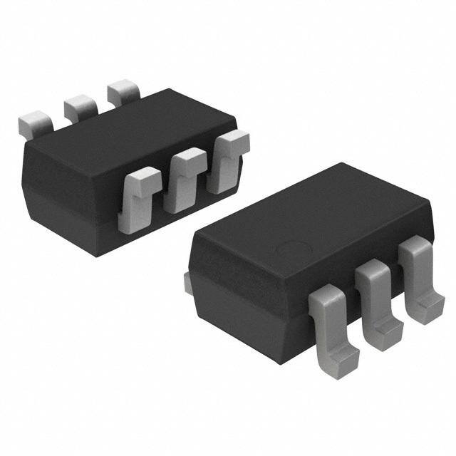
| 描述 | IC OP AMP HS W/FILTER SC-88多媒体杂项 SBN HFS - VIDEO AMP |
| 产品分类 | |
| 品牌 | ON Semiconductor |
| 产品手册 | |
| 产品图片 |
|
| rohs | 符合RoHS无铅 / 符合限制有害物质指令(RoHS)规范要求 |
| 产品系列 | 多媒体 IC,多媒体杂项,ON Semiconductor NCS2561SQT1G- |
| 数据手册 | |
| 产品型号 | NCS2561SQT1G |
| 产品种类 | 多媒体杂项 |
| 供应商器件封装 | SC-88/SC70-6/SOT-363 |
| 信噪比 | 70 dB |
| 其它名称 | NCS2561SQT1GOSCT |
| 包装 | 剪切带 (CT) |
| 压摆率 | - |
| 可用增益调整 | 6 dB |
| 商标 | ON Semiconductor |
| 安装类型 | 表面贴装 |
| 安装风格 | SMD/SMT |
| 封装 | Reel |
| 封装/外壳 | 6-TSSOP,SC-88,SOT-363 |
| 封装/箱体 | SC-88 |
| 工作电源电压 | 3.6 VDC |
| 工厂包装数量 | 3000 |
| 带宽 | 8 MHz |
| 应用 | |
| 最大工作温度 | + 125 C |
| 最小工作温度 | - 40 C |
| 标准包装 | 1 |
| 电压-电源,单/双 (±) | 2.7 V ~ 3.3 V |
| 电流-电源 | 6mA |
| 电流-输出/通道 | 50mA |
| 电源电流 | 6 mA |
| 电路数 | 1 |
| 类型 | Single Channel Video Driver |
| 系列 | NCS2561 |
| 输出类型 | - |
| 通道数量 | 1 Channel |


- 商务部:美国ITC正式对集成电路等产品启动337调查
- 曝三星4nm工艺存在良率问题 高通将骁龙8 Gen1或转产台积电
- 太阳诱电将投资9.5亿元在常州建新厂生产MLCC 预计2023年完工
- 英特尔发布欧洲新工厂建设计划 深化IDM 2.0 战略
- 台积电先进制程称霸业界 有大客户加持明年业绩稳了
- 达到5530亿美元!SIA预计今年全球半导体销售额将创下新高
- 英特尔拟将自动驾驶子公司Mobileye上市 估值或超500亿美元
- 三星加码芯片和SET,合并消费电子和移动部门,撤换高东真等 CEO
- 三星电子宣布重大人事变动 还合并消费电子和移动部门
- 海关总署:前11个月进口集成电路产品价值2.52万亿元 增长14.8%


PDF Datasheet 数据手册内容提取
NCS2561, NCV2561 3.3V Single Channel Video Driver with Recontruction Filter and SAG Correction The NCS2561 is a single high speed video driver including a 2−pole reconstruction filter and SAG correction capability. The NCS2561 is www.onsemi.com available in a space saving SC−88 package optimized for low voltage, portable applications. It is designed to be compatible with MARKING Digital−to−Analog Converters (DAC) embedded in most video processors. DIAGRAMS The NCS2561 internally integrates an 8 MHz 2−pole video DAC reconstruction filter with a fixed gain of 2. The NCS2561 also has a 6 1 built−in SAG correction circuit when used at the output in an SC−88 YG1 M(cid:2) AC−coupled mode. To further reduce power consumption, an enable SQ SUFFIX (cid:2) pin is provided. CASE 419B 1 Features • Internal 8 MHz 2−Pole Reconstruction Filter YG1 = Specific Device Code • Internal Fixed Gain: 6 dB M = Date Code* • (cid:2) = Pb−Free Package Integrated Level Shifter • (Note: Microdot may be in either location) SAG Correction Circuit for Reducing Coupling Capacitor Size *Date Code orientation and/or position may • Low Quiescent Current: 6 mA Typ vary depending upon manufacturing location. • Shutdown Current < 5 (cid:2)A • Wide Input Voltage Range PIN CONNECTIONS • Capability to Drive 2 CVBS Video Signals Together (2x150(cid:3) Loads) • Excellent Video Performance 1 6 • IN VCC Operating Supply Voltage Range: +2.7 V to +3.3 V 2 5 • GND Enable NCV Prefix for Automotive and Other Applications Requiring 3 4 Unique Site and Control Change Requirements; AEC−Q100 SAG OUT Qualified and PPAP Capable Top View • These Devices are Pb−Free and are RoHS Compliant Applications • ORDERING INFORMATION Portable Video, Digital Cameras & Camera Phones • Set−Top Box Video Filters Device Package Shipping† • NTSC and PAL NCS2561SQT1G SC−88 3000 / Tape & Reel (Pb−Free) Vcc 2.7V to 3.3V Enable NCV2561SQT1G SC−88 3000 / Tape & Reel (Pb−Free) 6 5 NCS2561 †For information on tape and reel specifications, including part orientation and tape sizes, please + refer to our Tape and Reel Packaging Specifications IN 1 Brochure, BRD8011/D. Level 2−pole 4 OUT Shifter filter − Related Resource: Refer to Application Note AND8457/D for details 3 SAG regarding SAG Correction 2 GND Figure 1. Block Diagram © Semiconductor Components Industries, LLC, 2011 1 Publication Order Number: August, 2018 − Rev. 4 NCS2561/D
NCS2561, NCV2561 PIN FUNCTION AND DESCRIPTION Pin Name Type Description 1 IN Input Video Input 2 GND Ground Ground 3 SAG Output Sag Compensation 4 OUT Output Video Output 5 Enable Input Enable / Disable Function: High = Enable, Low = Disable. When left open the default state is High. 6 VCC Power Power Supply / 2.7 V ≤ VCC ≤ 3.3 V ATTRIBUTES Characteristic Value ESD Protection (Note 1) Human Body Model 2 kV Machine Model 200 V Latch−up Current (Note 2) 75 mA Moisture Sensitivity (Note 3) Level 1 Flammability Rating Oxygen Index: 28 to 34 UL 94 V−0 @ 0.125 in 1. This device series incorporates ESD protection and is tested by the following methods: ESD Human Body Model tested per JEDEC standard JS−001−2017 (AEC−Q100−002) ESD Charged Device Model tested per JEDEC standard JS−002−2014 (AEC−Q100−011). 2. Latch−up Current tested per JEDEC standard JESD78E (AEC−Q100−004). 3. For additional Moisture Sensitivity information, refer to Application Note AND8003/D. MAXIMUM RATINGS Rating Symbol Value Unit Power Supply Voltages VCC 3.6 Vdc Input Voltage Range VI −0.5 to VCC + 0.5 Vdc Output Short−Circuit to GND thru 75 (cid:3) ISC Continuous − Maximum Junction Temperature (Note 4) TJ 150 °C Operating Ambient Temperature NCS2561 TA −40 to +125 °C NCV2561 (Note 5) −40 to +125 Storage Temperature Range Tstg −60 to +150 °C Thermal Resistance, Junction−to−Air R(cid:4)JA 250 °C/W Stresses exceeding those listed in the Maximum Ratings table may damage the device. If any of these limits are exceeded, device functionality should not be assumed, damage may occur and reliability may be affected. 4. Power dissipation must be considered to ensure maximum junction temperature (TJ) is not exceeded. 5. NCV prefix is for automotive and other applications requiring site and change control. MAXIMUM POWER DISSIPATION The maximum power that can be safely dissipated is soon as the die temperature is reduced. Leaving the device limited by the associated rise in junction temperature. For in the “overheated” condition for an extended period can the plastic packages, the maximum safe junction result in device burnout. To ensure proper operation, it is temperature is 150°C. If the maximum is exceeded important to observe the de−rating curves. momentarily, proper circuit operation will be restored as www.onsemi.com 2
NCS2561, NCV2561 DC ELECTRICAL CHARACTERISTICS with VCC = 2.7 V to 3.3 V (TA = +25°C, RL = 150 (cid:3) to GND, unless otherwise specified) Symbol Characteristic Conditions Min Typ Max Unit DC PERFORMANCE VOLS Offset Level−Shift Output Voltage VCC = 3.3 V, VIN = 0 V 10 60 80 mV TA = −40°C to +125°C (Note 6) 60 IIB Input Bias Current ±3 pA VIN Input Voltage Range (Note 7) VCC = 3.3 V GND VCC − 1.5 V AV Voltage Gain VCC = 3.3 V, 0 < VIN < 1.5 V 5.8 6.0 6.2 dB 40 IRE Sync, 100 IRE White Level VIH Enable Input High Level Voltage 1.6 VCC V VIL Enable Input Low Level Voltage GND 0.8 V OUTPUT CHARACTERISTICS VOH Output High Level Voltage RL = 150 (cid:3) to GND VCC − 0.3 VCC − 0.1 V RL = 75 (cid:3) to GND VCC − 0.3 VOL Output Low Level Voltage 60 mV (Note 8) IO Output Current VCC = 3.3 V ±50 mA POWER SUPPLY VCC Operating Voltage Range 2.7 3.3 V ICC, ON Power Supply Current − Enabled VIN = 0 V, VCC = 3.3 V, IO = 0 mA 6.0 7.5 mA TA = −40°C to +125°C (Note 6) 9.0 ICC, Power Supply Current − Disabled VIN = 0 V, VCC = 3.3 V, IO = 0 mA 1.5 5.0 (cid:2)A OFF PSRR Power Supply Rejection Ratio VCC = 2.7 V to 3.3 V ±80 (cid:2)V/V 6. Guaranteed by design and/or characterization. 7. Limited by output swing and internal gain. 8. Output low voltage level is limited by the internal level shift circuitry. AC ELECTRICAL CHARACTERISTICS with VCC = 2.7 V to 3.3 V (TA = +25°C, RL = 150 (cid:3) to GND, unless otherwise specified) Symbol Characteristic Conditions Min Typ Max Unit FREQUENCY DOMAIN PERFORMANCE An Normalized Passband Gain (Note VCC=3.3 V, f=1.0 MHz , VO=2 Vp−p −0.4 0 +0.4 dB 9) VCC=3.3 V, f=4.5 MHz , VO=2 Vp−p −0.2 +0.4 +0.8 f = 27 MHz, VO = 2 Vp−p −18 −22 dG Differential Gain VCC = 3.3 V, AV = +2, RL = 150 (cid:3)(cid:5) 0.5 % f = 3.58 MHz, 4.43 MHz dP Differential Phase VCC = 3.3 V, AV = +2, RL = 150 (cid:3), 1.0 ° f = 3.58 MHz, 4.43 MHz SNR Signal to Noise Ratio VCC = 3.3 V, 100% White Signal 70 dB TIME DOMAIN RESPONSE (cid:6)Tg Group Delay Variation VCC = 3.3 V, 100 kHz to 5.0 MHz 15 ns tON Turn ON Time 1.5 (cid:2)s tOFF Turn OFF Time 50 ns 9. The normalized gain is guaranteed by design and characterization. The max normalized gain of +0.8 dB is the result of smooth peaking (pre−emphasis, see figure 2) taking into account the increase of the losses at the highest frequencies into connectors and cable at the output. For frequencies lower than 2 MHz the max normalized gain is 0.4 dB. www.onsemi.com 3
NCS2561, NCV2561 TYPICAL CHARACTERISTICS (At TA = +25°C and RL = 150 (cid:3), unless otherwise specified) Figure 2. Frequency Response Figure 3. Group Delay vs. Frequency Figure 4. Differential Gain Figure 5. Differential Phase Figure 6. PSRR vs. Frequency Figure 7. Quiescent Current vs. Supply Voltage www.onsemi.com 4
NCS2561, NCV2561 Figure 8. Quiescent Current vs. Temperature Figure 9. Signal−to−Noise Ratio vs. Temperature (V = 3.0 V) CC www.onsemi.com 5
NCS2561, NCV2561 APPLICATIONS INFORMATION The NCS2561 is a single video driver optimized for To ensure the output signal is not clipped due to the lower portable applications with low power consumption in a rail limit, the NCS2561 has built−in level shift circuitry. The space saving SC−88 package. It includes sag correction role of this circuitry is to avoid clipping of the sync signal at circuitry allowing significant reduction of the AC−coupled the output by shifting up the video signal by about 60 mV. output capacitor. The level shift circuitry level shifts the sync signal above the internal op amp transistor saturation limit. This function is Internal Level Shift particularly useful when the video signal is DC−coupled at The input common mode voltage range (see the output. specifications V ) of the NCS2561 includes the lower rail IN (GND) and extends to VCC − 1.5V on a power supply range Built−in 2−Pole Reconstruction Filter of 2.7 V to 3.3 V. Many video processors operate with a The NCS2561 has a 2−pole reconstruction filter with a supply ranging from 0 V to a positive supply (typically −3 dB cut−off frequency at 8 MHz. The filter serves as an 3.3 V), so the lowest voltage of the video signal provided by anti−alias filter removing the unwanted over−sampling the DAC is 0 V. Although a 0 V (GND) signal is within the effects produced by the video DAC. The 27 MHz input common−mode range of the NCS2561, the output over−sampling frequency from the video DAC is attenuated signal will be limited, specifically at the lower rail. Op amps by 22 dB typical. In order to improve the stop−band use transistors with saturation voltage (Vsat) higher than attenuation a small capacitor (Cs) of a few tenths pico Farads 0 V. If the lowest level of the input voltage is lower than Vsat can be added in parallel with the source resistor (Rs) (See the signal will be clipped at the output. Figure 10). VCC 2.7V to 3.3V Enable 1 V p p 10 pF V Video 1 0 V IN 1.4 k(cid:3) + DAC 1.1 k(cid:3) 47 (cid:2)F / 67 (cid:2)F TV Rs 12 pF OUT 75 (cid:3) − Cs 845 (cid:3) 75 (cid:3) SAG 325 (cid:3) 528 (cid:3) 22 (cid:2)F Cs: Optional 650 (cid:3) NCS2561 GND Figure 10. Block Diagram Showing Filter and Sag Correction Circuits Shutdown Mode this video output is not permanently used and actually used If the Enable pin is left open by default the circuit will be in very specific period of time when pictures or small movies enabled. The Enable pin offers a shutdown function, so the want to be displayed on a bigger screen. The device’s NCS2561 can consequently be disabled when not used. This quiescent current drops typically down to 2.7 (cid:2)A when the is particularly important for digital still cameras or cell device is in the shutdown mode. phones with camera having a video output feature. Indeed www.onsemi.com 6
NCS2561, NCV2561 Sag Correction capacitors, and a coupling configuration to saving space. Video drivers that do not incorporate sag compensation The sag compensation circuitry allows the reduction of this traditionally recommend a large coupling capacitor (220 (cid:2)F) output coupling capacitor value by inducing peaking at the on the output of the video driver. Larger output coupling lower cutoff frequency of the high pass filter. The high−pass capacitors (≥ 470 (cid:2)F) are often chosen by design engineers filter is created by the coupling capacitor and the load when the application allows this (Set−Top Box). A larger resistor (1/(2(cid:7)R Cout), and this peaking lowers the cutoff L output coupling capacitor allows a lower cut−off frequency frequency. Simulation results provided in Figure 11 show to avoid field tilt effects; however in portable applications the effect of the sag compensation at the low cut−off there is a trade−off between large and expensive coupling frequency. Gain VS Frequency 20 15 10 5 B) 0 d n ( −5 Gai −10 −15 −20 −25 −30 1 10 100 1000 10000 100000 100000010000000 1E+08 Frequency (Hz) Cout = 22uF Cout = 47uF Cout = 67uF Cout = 100uF Cout = 220uF Figure 11. Simulation Results with Csag = 22 (cid:2)F and Variable Cout Calculations show that a 220 (cid:2)F output capacitor frequency; the cut−off frequency will be in the critical 50 Hz produces a low cutoff frequency of 5 Hz, and a 470(cid:8)(cid:2)F or 60 Hz frequencies. This undesirable affect will manifest capacitor will give a low cutoff frequency at 2.6 Hz. The itself as field tilt. Due to the SAG correction the large output cutoff frequency (−3 dB) is defined by the equation: capacitor is reduced without degrading the video 1/(2(cid:7)R Cout). In the case where no sag is used (Figure 14), performances by the use of two smaller and cheaper output L a low Cout value can adversely affect the low cutoff capacitors. Vcc 2.7V to 3.3V Enable 1 V NCS2561 Vcc Enable p p V VDidAeCo 1 0 V IN + OUT47 (cid:2)F / 67 (cid:2)F TV Level 2−pole Rs Shifter filter 75 (cid:3) − 75 (cid:3) SAG 22 (cid:2)F GND Figure 12. Sag Correction Configuration www.onsemi.com 7
NCS2561, NCV2561 The Csag value has no significant impact on the coupling Figures 13 and 14 show the impact of the output coupling even as the value increases. A value of 22 (cid:2)F is capacitor on a video signal corresponding to a worst case recommended for optimal performance. situation regarding the low frequency bandwidth. The video To achieve similar behavior to an output coupling signal used is a 50 Hz 1/2 black − 1/2 white video pattern. capacitor value Cout = 220 (cid:2)F (no sag) the nominal This signal is obtained using the PAL Flat Field Square wave equivalent sag combination is Csag = 22 (cid:2)F and Cout = signal option available with the video generator TG700 from 67(cid:8)(cid:2)F. A value of 47(cid:8)(cid:2)F for Cout will yield equivalent Tektronix. These measurements show how the sag function results. If we consider a coupling cap of 470 (cid:2)F, the best can help to reduce the field tilt problem using lower value compromise for sag combination is Csag = 22 (cid:2)F and Cout coupling capacitor than traditional approach. = 100 (cid:2)F. A value of 67(cid:8)(cid:2)F for Cout will yield equivalent results. Figure 13. No sag, Cout = 220 (cid:2)F Figure 14. Csag = 22 (cid:2)F, Cout = 47 (cid:2)F (Top : Input, Bottom : Output) (Top : Input, Bottom : Output) Vcc 2.7V to 3.3V Enable 1 V NCS2561 Vcc Enable p p V VDidAeCo 1 0 V IN + OUT 220(cid:2)F / 470(cid:2)F TV Level 2−pole Rs Shifter filter 75 (cid:3) − 75 (cid:3) SAG GND Figure 15. NCS2561 in an AC−Coupled Configuration with no sag www.onsemi.com 8
NCS2561, NCV2561 DC−Coupled Output The problems of field tilt effects on the video signal are Having efficient output AC−coupled capability thanks to also eliminated providing the best video quality with the sag correction option, with the built−in level shifter, the optimal dynamic or peak−to−peak amplitude of the video NCS2561 can also be DC−coupled to a 150 (cid:3) load. This has signal allowing operating at the lower power supply voltage the advantage of eliminating the AC−coupling capacitors at (2.7 V) without risk of signal clipping. In this coupling the output by reducing the number of external components configuration the average output voltage is higher than 0 V and saving space on the board. This can be a key advantage and the power consumption can be a little higher than with for some portable applications with limited space. an AC−coupled configuration. Vcc 2.7V to 3.3V Enable 1 V NCS2561 Vcc Enable p p V Video 1 0 V IN + TV DAC OUT Level 2−pole Rs Shifter filter 75 (cid:3) − 75 (cid:3) SAG GND Figure 16. DC−Coupled Input and Output Configuration Video Driving Capability applications is illustrated in the Figure 17. Figure 18 With an output current capability of ±50 mA the NSC2561 (multiburst) and Figure 19 (linearity) show that the video was designed to be able to drive at least 2 video display loads signal can efficiently drive a 75 (cid:3) equivalent load and not in parallel (2 different display or 1 display + 1 VCR). This degrade the video performance. Vcc 2.7V to 3.3V Enable 1 V NCS2561 Vcc Enable p p Video 1 V0 V IN + 4677 (cid:2) (cid:2)FF / 75 (cid:3) DAC OUT TV Level 2−pole Rs Shifter filter 75 (cid:3) − Other Video SAG 22 (cid:2)F 75 (cid:3) Display 75 (cid:3) GND Figure 17. NCS2561 Driving 2 Video Display (two 150 (cid:3) loads) www.onsemi.com 9
NCS2561, NCV2561 Figure 18. Multiburst Test with two 150 (cid:3) loads Figure 19. Linearity Test with two 150 (cid:3) loads ESD Protection more than 4 kV has been measured on this specific output All the device pins are protected against electrostatic pin. This feature is particularly important for video driver discharge at a level of 2 kV HBM. The output has been which usually constitutes the last stage in the video chain considered with a particular attention with ESD structure before the video output connector. able to sustain typically more than 2 kV HBM. Actually www.onsemi.com 10
NCS2561, NCV2561 PACKAGE DIMENSIONS SC−88/SC70−6/SOT−363 CASE 419B−02 ISSUE Y 2X aaa H D D H N1O.TDEISM:ENSIONING AND TOLERANCING PER ASME Y14.5M, 1994. 2. CONTROLLING DIMENSION: MILLIMETERS. A 3. DIMENSIONS D AND E1 DO NOT INCLUDE MOLD FLASH, D PROTRUSIONS, OR GATE BURRS. MOLD FLASH, PROTRU- GAGE PLANE SIONS, OR GATE BURRS SHALL NOT EXCEED 0.20 PER END. 4. DIMENSIONS D AND E1 AT THE OUTERMOST EXTREMES OF 6 5 4 THE PLASTIC BODY AND DATUM H. L2 L 5. DATUMS A AND B ARE DETERMINED AT DATUM H. E E1 6. DIMENSIONS b AND c APPLY TO THE FLAT SECTION OF THE DETAIL A LEAD BETWEEN 0.08 AND 0.15 FROM THE TIP. 7. DIMENSION b DOES NOT INCLUDE DAMBAR PROTRUSION. 1 2 3 ALLOWABLE DAMBAR PROTRUSION SHALL BE 0.08 TOTAL IN aaa C EXCESS OF DIMENSION b AT MAXIMUM MATERIAL CONDI- 2X TION. THE DAMBAR CANNOT BE LOCATED ON THE LOWER bbb H D 2X 3 TIPS RADIUS OF THE FOOT. e MILLIMETERS INCHES B 6X b DIM MIN NOM MAX MIN NOM MAX A −−− −−− 1.10 −−− −−− 0.043 TOP VIEW ddd M C A-B D AA12 00..0700 0−.−9−0 10..0100 00..000207 0.−0−35− 00..000349 b 0.15 0.20 0.25 0.006 0.008 0.010 C 0.08 0.15 0.22 0.003 0.006 0.009 A2 DETAIL A D 1.80 2.00 2.20 0.070 0.078 0.086 A E 2.00 2.10 2.20 0.078 0.082 0.086 E1 1.15 1.25 1.35 0.045 0.049 0.053 e 0.65 BSC 0.026 BSC L 0.26 0.36 0.46 0.010 0.014 0.018 L2 0.15 BSC 0.006 BSC aaa 0.15 0.006 bbb 0.30 0.012 6X ccc C ccc 0.10 0.004 A1 ddd 0.10 0.004 C SEATING c PLANE SIDE VIEW END VIEW RECOMMENDED SOLDERING FOOTPRINT* 6X 6X 0.30 0.66 2.50 0.65 PITCH DIMENSIONS: MILLIMETERS *For additional information on our Pb−Free strategy and soldering details, please download the ON Semiconductor Soldering and Mounting Techniques Reference Manual, SOLDERRM/D. ON Semiconductor and are trademarks of Semiconductor Components Industries, LLC dba ON Semiconductor or its subsidiaries in the United States and/or other countries. ON Semiconductor owns the rights to a number of patents, trademarks, copyrights, trade secrets, and other intellectual property. A listing of ON Semiconductor’s product/patent coverage may be accessed at www.onsemi.com/site/pdf/Patent−Marking.pdf. ON Semiconductor reserves the right to make changes without further notice to any products herein. ON Semiconductor makes no warranty, representation or guarantee regarding the suitability of its products for any particular purpose, nor does ON Semiconductor assume any liability arising out of the application or use of any product or circuit, and specifically disclaims any and all liability, including without limitation special, consequential or incidental damages. Buyer is responsible for its products and applications using ON Semiconductor products, including compliance with all laws, regulations and safety requirements or standards, regardless of any support or applications information provided by ON Semiconductor. “Typical” parameters which may be provided in ON Semiconductor data sheets and/or specifications can and do vary in different applications and actual performance may vary over time. All operating parameters, including “Typicals” must be validated for each customer application by customer’s technical experts. ON Semiconductor does not convey any license under its patent rights nor the rights of others. ON Semiconductor products are not designed, intended, or authorized for use as a critical component in life support systems or any FDA Class 3 medical devices or medical devices with a same or similar classification in a foreign jurisdiction or any devices intended for implantation in the human body. Should Buyer purchase or use ON Semiconductor products for any such unintended or unauthorized application, Buyer shall indemnify and hold ON Semiconductor and its officers, employees, subsidiaries, affiliates, and distributors harmless against all claims, costs, damages, and expenses, and reasonable attorney fees arising out of, directly or indirectly, any claim of personal injury or death associated with such unintended or unauthorized use, even if such claim alleges that ON Semiconductor was negligent regarding the design or manufacture of the part. ON Semiconductor is an Equal Opportunity/Affirmative Action Employer. This literature is subject to all applicable copyright laws and is not for resale in any manner. PUBLICATION ORDERING INFORMATION LITERATURE FULFILLMENT: N. American Technical Support: 800−282−9855 Toll Free ON Semiconductor Website: www.onsemi.com Literature Distribution Center for ON Semiconductor USA/Canada 19521 E. 32nd Pkwy, Aurora, Colorado 80011 USA Europe, Middle East and Africa Technical Support: Order Literature: http://www.onsemi.com/orderlit Phone: 303−675−2175 or 800−344−3860 Toll Free USA/Canada Phone: 421 33 790 2910 Fax: 303−675−2176 or 800−344−3867 Toll Free USA/Canada For additional information, please contact your local Email: orderlit@onsemi.com Sales Representative ◊ www.onsemi.com NCS2561/D 11
Mouser Electronics Authorized Distributor Click to View Pricing, Inventory, Delivery & Lifecycle Information: O N Semiconductor: NCS2561SQT1G NCV2561SQT1G