ICGOO在线商城 > 集成电路(IC) > PMIC - 稳压器 - 线性 > NCP571MN10TBG
 Datasheet下载
- 型号: NCP571MN10TBG
- 制造商: ON Semiconductor
- 库位|库存: xxxx|xxxx
- 要求:
| 数量阶梯 | 香港交货 | 国内含税 |
| +xxxx | $xxxx | ¥xxxx |
查看当月历史价格
查看今年历史价格
NCP571MN10TBG产品简介:
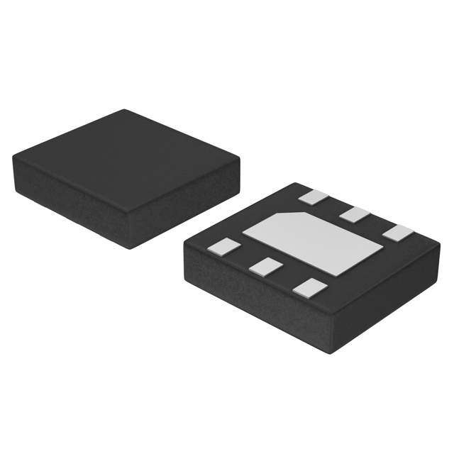
ICGOO电子元器件商城为您提供NCP571MN10TBG由ON Semiconductor设计生产,在icgoo商城现货销售,并且可以通过原厂、代理商等渠道进行代购。 NCP571MN10TBG价格参考。ON SemiconductorNCP571MN10TBG封装/规格:PMIC - 稳压器 - 线性, Linear Voltage Regulator IC 正,固定式 1 Output 150mA 6-DFN(2x2.2)。您可以下载NCP571MN10TBG参考资料、Datasheet数据手册功能说明书,资料中有NCP571MN10TBG 详细功能的应用电路图电压和使用方法及教程。
| 参数 | 数值 |
| 产品目录 | 集成电路 (IC) |
| 描述 | IC REG LDO 1V 0.15A 6DFN |
| 产品分类 | |
| 品牌 | ON Semiconductor |
| 数据手册 | |
| 产品图片 |
|
| 产品型号 | NCP571MN10TBG |
| PCN设计/规格 | |
| rohs | 无铅 / 符合限制有害物质指令(RoHS)规范要求 |
| 产品系列 | - |
| 供应商器件封装 | 6-DFN(2x2.2) |
| 其它名称 | NCP571MN10TBGOSTR |
| 包装 | 带卷 (TR) |
| 安装类型 | 表面贴装 |
| 封装/外壳 | 6-VDFN 裸露焊盘 |
| 工作温度 | -40°C ~ 85°C |
| 标准包装 | 3,000 |
| 电压-跌落(典型值) | 0.55V @ 10mA |
| 电压-输入 | 最高 12V |
| 电压-输出 | 1V |
| 电流-输出 | 150mA |
| 电流-限制(最小值) | - |
| 稳压器拓扑 | 正,固定式 |
| 稳压器数 | 1 |


- 商务部:美国ITC正式对集成电路等产品启动337调查
- 曝三星4nm工艺存在良率问题 高通将骁龙8 Gen1或转产台积电
- 太阳诱电将投资9.5亿元在常州建新厂生产MLCC 预计2023年完工
- 英特尔发布欧洲新工厂建设计划 深化IDM 2.0 战略
- 台积电先进制程称霸业界 有大客户加持明年业绩稳了
- 达到5530亿美元!SIA预计今年全球半导体销售额将创下新高
- 英特尔拟将自动驾驶子公司Mobileye上市 估值或超500亿美元
- 三星加码芯片和SET,合并消费电子和移动部门,撤换高东真等 CEO
- 三星电子宣布重大人事变动 还合并消费电子和移动部门
- 海关总署:前11个月进口集成电路产品价值2.52万亿元 增长14.8%


PDF Datasheet 数据手册内容提取
NCP571, NCV571 150 mA CMOS Low Iq Low Output Voltage Regulator The NCP571 series of fixed output low dropout linear regulators are designed for handheld communication equipment and portable battery powered applications which require low quiescent current. The NCP571 series features an ultra−low quiescent current of 4.0 (cid:2)A. http://onsemi.com Each device contains a voltage reference unit, an error amplifier, a PMOS power transistor, resistors for setting output voltage, current 6 limit, and temperature limit protection circuits. 5 The NCP571 has been designed to be used with low cost ceramic capacitors and requires a minimum output capacitor of 0.1 (cid:2)F. The 1 1 device is housed in the TSOP−5 or DFN6 surface mount package. TSOP−5 DFN6 Standard voltage versions are 0.8 V, 0.9 V, 1.0 V and 1.2 V. SN SUFFIX MN SUFFIX CASE 483 CASE 506BA Features • Low Quiescent Current of 4.0 (cid:2)A Typical • Maximum Operating Voltage of 12 V MARKING DIAGRAMS • Low Output Voltage Option down to 0.8 V • High Accuracy Output Voltage of 3.0% • Industrial Temperature Range of −40°C to +85°C XXXAYW(cid:2) 1 XX M(cid:2) (NCV571, T = −40°C to +125°C) (cid:2) (cid:2) A • NCV Prefix for Automotive and Other Applications Requiring Unique Site and Control Change Requirements; AEC−Q100 Qualified and PPAP Capable • XXX = Specific Device Code These are Pb−Free Devices A = Assembly Location Y = Year Typical Applications W = Work Week • Battery Powered Instruments M = Date Code • (cid:2) = Pb−Free Package Hand−Held Instruments • (Note: Microdot may be in either location) Camcorders and Cameras Vin Vout 1 5 ORDERING INFORMATION See detailed ordering and shipping information in the package Driver w/ dimensions section on page 9 of this data sheet. Thermal Current Shutdown Limit + Enable 3 ON OFF GND 2 Figure 1. Representative Block Diagram © Semiconductor Components Industries, LLC, 2014 1 Publication Order Number: June, 2014 − Rev. 5 NCP571/D
NCP571, NCV571 PIN CONNECTIONS TSOP−5 package DFN6 package Vin 1 5 Vout Vout 1 6 Vin GND 2 NC 2 EP 5 NC Enable 3 4 NC GND 3 4 Enable (Top View) (Top View) PIN FUNCTION DESCRIPTION DFN6 TSOP−5 Pin Name Description 1 5 Vout Regulated output voltage. 2 4 NC No Internal Connection. It is recommended to connect this pin to GND potential. 3 2 GND Power supply ground. 4 3 Enable This input is used to place the device into low−power standby. When this input is pulled low, the device is disabled. If this function is not used, Enable pin should be connected to Vin. 5 − NC No Internal Connection. It is recommended to connect this pin to GND potential. 6 1 Vin Positive power supply input voltage. EP − EP No Internal Connection. It is recommended to connect this pin to GND potential. MAXIMUM RATINGS Rating Symbol Value Unit Input Voltage Vin 0 to 12 V Enable Voltage VEN −0.3 to Vin + 0.3 V Output Voltage Vout −0.3 to Vin + 0.3 V Power Dissipation PD Internally Limited W Operating Junction Temperature TJ +150 °C Operating Ambient Temperature NCP571 TA −40 to +85 °C NCV571 −40 to +125 Storage Temperature Tstg −55 to +150 °C ESD Capability, Human Body Model (Note 1) ESDHBM 2000 V ESD Capability, Machine Mode (Note 1) ESDMM 200 V ESD Capability, Charged Device Model (Note 1) ESDCDM 1000 V Stresses exceeding Maximum Ratings may damage the device. Maximum Ratings are stress ratings only. Functional operation above the Recommended Operating Conditions is not implied. Extended exposure to stresses above the Recommended Operating Conditions may affect device reliability. 1. This device series contains ESD protection and exceeds the following tests: ESD Human Body Model tested per AEC−Q100−002 (EIA/JESD22−A114) ESD Machine Model tested per AEC−Q100−003 (EIA/JESD22−A115) ESD Charged Device Model tested per EIA/JES D22/C101, Field Induced Charge Model (Jedec Standard) 2. Latchup capability (85°C) (cid:2)100 mA DC with trigger voltage. THERMAL CHARACTERISTICS Rating Symbol Test Conditions Typical Value Unit Junction−to−Ambient TSOP−5 R(cid:3)JA 1 oz Copper Thickness, 100 mm2 250 °C/W PSIJ−Lead 2 TSOP−5 (cid:4) 1 oz Copper Thickness, 100 mm2 68 °C/W J−L2 Junction−to−Ambient DFN6 R(cid:3)JA 1 oz Copper Thickness, 100 mm2 190 °C/W PSIJ−Lead 2 DFN6 (cid:4) 1 oz Copper Thickness, 100 mm2 84 °C/W J−L2 NOTE: Single component mounted on an 80 x 80 x 1.5 mm FR4 PCB with stated copper head spreading area. Using the following boundary conditions as stated in EIA/JESD 51−1, 2, 3, 7, 12. http://onsemi.com 2
NCP571, NCV571 Vin 1 Vin Vout 5 Vout 4 NC 2 3 C1 GND EN C2 0.1 (cid:2)F 0.1 (cid:2)F GND GND Enable Figure 2. Typical Application Schematic for TSOP−5 Package ELECTRICAL CHARACTERISTICS (Vin = Vout(nom) + 1.0 V, VEN = Vin, Cin = 1.0 (cid:2)F, Cout = 1.0 (cid:2)F, TA = 25°C, unless otherwise noted) Characteristic Symbol Min Typ Max Unit Output Voltage (TA = 25°C, Iout = 10 mA) Vout − 3% + 3% V 0.8 V 0.776 0.8 0.824 0.9 V 0.873 0.9 0.927 1.0 V 0.970 1.0 1.030 1.2 V 1.164 1.2 1.236 Output Voltage (TA = −40°C to +85°C for NCP571 or TA = −40°C to Vout − 4% + 4% V +125°C for NCV571, Iout = 10 mA) (Note 5) 0.8 V 0.768 0.8 0.832 0.9 V 0.864 0.9 0.936 1.0 V 0.960 1.0 1.040 1.2 V 1.152 1.2 1.248 Line Regulation (Vin = Vout + 1.0 V to 12 V, Iout = 10 mA) Regline − 10 30 mV Load Regulation (Iout = 10 mA to 150 mA, Vin = Vout + 2.0 V) Regload − 40 65 mV Output Current (Vout = (Vout at Iout = 100 mA) − 3%) Io(nom) mA 0.8 V (Vin = 3.0 V) 150 − − 0.9 V (Vin = 3.0 V) 150 − − 1.0 V (Vin = 3.0 V) 150 − − 1.2 V (Vin = 3.0 V) 150 − − Dropout Voltage (Iout = 10 mA, Measured at Vout − 3.0%) Vin−Vout mV 0.8 V − 730 850 0.9 V − 650 750 1.0 V − 550 650 1.2 V − 350 450 Quiescent Current IQ uA (Enable Input = 0 V) − 0.1 1.0 (Enable Input = Vin = 3 V, Iout = 1.0 mA to 150 mA and − 4.0 8.0 Vin = Enable Input = 3 V, Iout = 150 mA) Output Voltage Temperature Coefficient Tc − 100 − ppm/°C Enable Input Threshold Voltage Vth(en) V (Voltage Increasing, Output Turns On, Logic High) 1.3 − − (Voltage Decreasing, Output Turns Off, Logic Low) − − 0.3 Output Short Circuit Current (Vout = 0 V) (Note 4) Iout(max) mA 0.8 V (Vin = 3.0 V) 160 260 600 0.9 V (Vin = 3.0 V) 160 260 600 1.0 V (Vin = 3.0 V) 160 260 600 1.2 V (Vin = 3.0 V) 160 260 600 3. Maximum package power dissipation limits must be observed. T (cid:4)T P (cid:3) J(max) A D R (cid:3)JA 4. Low duty cycle pulse techniques are used during testing to maintain the junction temperature as close to ambient as possible. http://onsemi.com 3
NCP571, NCV571 5. NCP571 Tlow = −40°C Thigh = +85°C NCV571 Tlow = −40°C Thigh = +125°C. 3.2 3.2 A) 3.0 Vin = 6 V A) 3.0 (cid:2) (cid:2) T ( T ( N N E 2.8 E 2.8 R Vin = 3 V R R R U U Vin = 6 V C C D 2.6 D 2.6 N N OU OU Vin = 3 V GR 2.4 GR 2.4 TA = 25°C TA = 25°C Vout = 0.8 V Vout = 1.2 V 2.2 2.2 0.00 0.02 0.04 0.06 0.08 0.10 0.12 0.14 0.16 0.00 0.02 0.04 0.06 0.08 0.10 0.12 0.14 0.16 OUTPUT CURRENT (A) OUTPUT CURRENT (A) Figure 3. Ground Pin Current vs. Output Figure 4. Ground Pin Current vs. Output Current Current 3.5 3.5 (cid:2)A) 3.0 Vin = 6 V (cid:2)A) 3.0 T ( T ( N N E E R R UR 2.5 Vin = 3 V UR 2.5 Vin = 6 V C C ND ND Vin = 3 V U U O 2.0 O 2.0 R R G Vout = 0.8 V G Iout = 30 mA Vout = 1.2 V Iout = 30 mA 1.5 1.5 −40 −20 0 20 40 60 80 100 −40 −20 0 20 40 60 80 100 AMBIENT TEMPERATURE (°C) AMBIENT TEMPERATURE (°C) Figure 5. Ground Pin Current vs. Temperature Figure 6. Ground Pin Current vs. Temperature 3.5 3 3 2.5 A) A) (cid:2) 2.5 (cid:2) T ( T ( 2 N N E 2 E R R R R 1.5 U U C 1.5 C D D N N 1 U 1 U O O GR 0.5 TA = 25°C GR 0.5 TA = 25°C Vout = 0.8 V Vout = 1.2 V Iout = 30 mA Iout = 30 mA 0 0 0 2 4 6 8 10 12 0 2 4 6 8 10 12 INPUT VOLTAGE (V) INPUT VOLTAGE (V) Figure 7. Ground Pin Current vs. Input Voltage Figure 8. Ground Pin Current vs. Input Voltage http://onsemi.com 4
NCP571, NCV571 1.0 1.4 TA = 25°C TA = 25°C 1.2 0.8 V) V) E ( E ( 1.0 G G LTA 0.6 Iout = 70 mA LTA 0.8 Iout = 70 mA O O UT V 0.4 Iout = 10 mA UT V 0.6 Iout = 10 mA P P T T 0.4 OU 0.2 Iout = 150 mA OU Iout = 150 mA 0.2 0.0 0.0 0 2 4 6 8 10 12 0 2 4 6 8 10 12 INPUT VOLTAGE (V) INPUT VOLTAGE (V) Figure 9. Output Voltage vs. Input Voltage Figure 10. Output Voltage vs. Input Voltage Figure 11. Line Transient Response Figure 12. Line Transient Response 3 V to 4 V Figure 13. Line Transient Response Figure 14. Line Transient Response http://onsemi.com 5
NCP571, NCV571 Figure 15. Load Transient Response Figure 16. Load Transient Response VENA VENA: 1 V/div VENA VENA: 1 V/div Figure 17. Enable Operation Figure 18. Enable Operation http://onsemi.com 6
NCP571, NCV571 APPLICATIONS INFORMATION A typical application circuit for the NCP571 series is without fear of instabilities. Larger values improve noise shown in Figure 2. rejection and load regulation transient response. Input Decoupling (C1) Enable Operation A 0.1 (cid:2)F capacitor either ceramic or tantalum is The enable pin will turn on or off the regulator. These recommended and should be connected close to the NCP571 limits of threshold are covered in the electrical specification package. Higher values and lower ESR will improve the section of this data sheet. If the enable is not used then the overall line transient response. pin should be connected to V . It is not recommended to in leave this pin on air. In case the voltage of Enable signal is Output Decoupling (C2) higher then Input voltage of NCP571 device it is necessary The NCP571 is a stable Regulator and does not require add an resistor divider in order to keep voltage at Enable pin any specific Equivalent Series Resistance (ESR) or a bellow Input voltage. A single gate device of VHC family minimum output current. Capacitors exhibiting ESRs could be used for this logic level translation. The NL17SZ06 ranging from a few m(cid:5) up to 3.0 (cid:5) can thus safely be used. device could be chosen for non inverting open−drain buffer The minimum decoupling value is 0.1 (cid:2)F and can be as shown in Figure 19. Other possibility is using NL17SZ16 augmented to fulfill stringent load transient requirements. device as shown in Figure 20. More information is The regulator accepts ceramic chip capacitors as well as mentioned in Application Note AND8101/D. tantalum devices. Larger output capacitors can be used NCP571 Vin Vin Vout Vout NC C1 GND Enable C2 0.1 (cid:2)F 0.1 (cid:2)F GND GND 3.3 V 3.3 V 0 V Enable NL17SZ06 Figure 19. http://onsemi.com 7
NCP571, NCV571 NCP571 2.7 V Vin Vin Vout Vout NC C1 GND Enable C2 0.1 (cid:2)F 0.1 (cid:2)F GND GND 3.3 V 2.7 V 0 V 0 V Enable NL17SZ16 Figure 20. Hints conductivity through the PCB, the junction temperature will Please be sure the Vin and GND lines are sufficiently wide. be relatively low with high power dissipation applications. When the impedance of these lines is high, there is a chance The maximum dissipation the package can handle is given to pick up noise or cause the regulator to malfunction. by: Set external components, especially the output capacitor, T (cid:4)T as close as possible to the circuit, and make leads as short as P (cid:3) J(max) A D R possible. (cid:3)JA If junction temperature is not allowed above the Thermal maximum 125°C, then the NCP571 can dissipate up to As power across the NCP571 increases, it might become 400 mW @ 25°C. necessary to provide some thermal relief. The maximum The power dissipated by the NCP571 can be calculated power dissipation supported by the device is dependent from the following equation: upon board design and layout. Mounting pad configuration (cid:5) (cid:7) P (cid:3)V I (cid:6)I (cid:4)V *I on the PCB, the board material, and also the ambient tot in(max) GND out out out temperature effect the rate of temperature rise for the part. If a 150 mA output current is needed then the ground This is stating that when the NCP571 has good thermal current from the data sheet is 4.0 (cid:2)A. http://onsemi.com 8
NCP571, NCV571 ORDERING INFORMATION Nominal Device Output Voltage Marking Package Shipping† NCP571SN08T1G 0.8 N6A TSOP−5 3000 / Tape & Reel (Pb−Free) NCP571SN09T1G 0.9 N6E TSOP−5 3000 / Tape & Reel (Pb−Free) NCP571SN10T1G 1.0 N6C TSOP−5 3000 / Tape & Reel (Pb−Free) NCP571SN12T1G 1.2 N6D TSOP−5 3000 / Tape & Reel (Pb−Free) NCV571SN08T1G* 0.8 N6F TSOP−5 3000 / Tape & Reel (Pb−Free) NCV571SN09T1G* 0.9 N6G TSOP−5 3000 / Tape & Reel (Pb−Free) NCV571SN10T1G* 1.0 N6H TSOP−5 3000 / Tape & Reel (Pb−Free) NCV571SN12T1G* 1.2 N6J TSOP−5 3000 / Tape & Reel (Pb−Free) NCP571MN08TBG 0.8 AC DFN6 3000 / Tape & Reel (Pb−Free) NCP571MN09TBG 0.9 AD DFN6 3000 / Tape & Reel (Pb−Free) NCP571MN10TBG 1.0 AE DFN6 3000 / Tape & Reel (Pb−Free) NCP571MN12TBG 1.2 AA DFN6 3000 / Tape & Reel (Pb−Free) NCV571MN08TBG* 0.8 AF DFN6 3000 / Tape & Reel (Pb−Free) NCV571MN09TBG* 0.9 AG DFN6 3000 / Tape & Reel (Pb−Free) NCV571MN10TBG* 1.0 AH DFN6 3000 / Tape & Reel (Pb−Free) NCV571MN12TBG* 1.2 AJ DFN6 3000 / Tape & Reel (Pb−Free) †For information on tape and reel specifications, including part orientation and tape sizes, please refer to our Tape and Reel Packaging Specifications Brochure, BRD8011/D. *NCV Prefix for Automotive and Other Applications Requiring Unique Site and Control Change Requirements; AEC−Q100 Qualified and PPAP Capable. http://onsemi.com 9
NCP571, NCV571 PACKAGE DIMENSIONS TSOP−5 CASE 483−02 ISSUE K NOTES: 1. DIMENSIONING AND TOLERANCING PER ASME NOTE 5 D5X Y14.5M, 1994. 2. CONTROLLING DIMENSION: MILLIMETERS. 0.20 C A B 3. MAXIMUM LEAD THICKNESS INCLUDES LEAD FINISH 2X 0.10 T THICKNESS. MINIMUM LEAD THICKNESS IS THE MINIMUM THICKNESS OF BASE MATERIAL. M 4. DIMENSIONS A AND B DO NOT INCLUDE MOLD 2X 0.20 T B 5 4 S FFLLAASSHH,, PPRROOTTRRUUSSIIOONNSS,, OORR GGAATTEE BBUURRRRSS. SMHOALLDL NOT 1 2 3 EXCEED 0.15 PER SIDE. DIMENSION A. K 5. OPTIONAL CONSTRUCTION: AN ADDITIONAL B G DETAIL Z TTRRIIMMMMEEDD LLEEAADD INSO ATL TLOO WEXETDE INND T HMIOS RLEO CTHATAINO N0..2 A A FROM BODY. MILLIMETERS TOP VIEW DIM MIN MAX A 3.00 BSC B 1.50 BSC DETAIL Z C 0.90 1.10 J D 0.25 0.50 C G 0.95 BSC H 0.01 0.10 0.05 J 0.10 0.26 H C SPELAATNIENG END VIEW MK 0.02 0(cid:3) 010.6 (cid:3) 0 SIDE VIEW S 2.50 3.00 SOLDERING FOOTPRINT* 1.9 0.074 0.95 0.037 2.4 0.094 1.0 0.039 0.7 (cid:5) (cid:7) 0.028 SCALE 10:1 mm inches *For additional information on our Pb−Free strategy and soldering details, please download the ON Semiconductor Soldering and Mounting Techniques Reference Manual, SOLDERRM/D. http://onsemi.com 10
NCP571, NCV571 PACKAGE DIMENSIONS DFN6, 2x2.2, 0.65P CASE 506BA ISSUE A D A L L NOTES: 1. DIMENSIONING AND TOLERANCING PER B ASME Y14.5M, 1994. 2. CONTROLLING DIMENSION: MILLIMETERS. L1 3. DIMENSION b APPLIES TO PLATED TERMINAL AND IS MEASURED BETWEEN 0.15 AND 0.20 mm FROM TERMINAL. DETAIL A 4. COPLANARITY APPLIES TO THE EXPOSED ÉÉÉ E PAD AS WELL AS THE TERMINALS. PIN ONE ALTERNATE TERMINAL REFERENCE ÉÉÉ CONSTRUCTIONS MILLIMETERS DIM MIN MAX 2X A 0.80 1.00 0.10 C A3 A1 0.00 0.05 TOP VIEW EXPOSED Cu MOLD CMPD b 0.20 0.30 ÉÉ ÉÇÉÇ 2X D 2.00 BSC 0.10 C ÉÉ ÇÇ DE2 1.21.020 BS1.C30 A A1 Ee2 0.07.065 BS0.C90 0.10 C DETAIL B DETAIL B K 0.20 −−− ALTERNATE L 0.25 0.35 CONSTRUCTIONS L1 0.00 0.10 7X 0.08 C SOLDERING FOOTPRINT* SIDE VIEW A1 C SPELAATNIENG 1.36 06X.58 PACKAGE OUTLINE D2 DETAIL A e 6XL 6X L1 1 3 0.96 2.50 E2 1 K 6 4 6Xb 6X 0.65 0.35 PITCH BOTTOM VIEW 0.10 C A B DIMENSIONS: MILLIMETERS 0.05 C NOTE 3 *For additional information on our Pb−Free strategy and soldering details, please download the ON Semiconductor Soldering and Mounting Techniques Reference Manual, SOLDERRM/D. ON Semiconductor and are registered trademarks of Semiconductor Components Industries, LLC (SCILLC). SCILLC owns the rights to a number of patents, trademarks, copyrights, trade secrets, and other intellectual property. A listing of SCILLC’s product/patent coverage may be accessed at www.onsemi.com/site/pdf/Patent−Marking.pdf. SCILLC reserves the right to make changes without further notice to any products herein. SCILLC makes no warranty, representation or guarantee regarding the suitability of its products for any particular purpose, nor does SCILLC assume any liability arising out of the application or use of any product or circuit, and specifically disclaims any and all liability, including without limitation special, consequential or incidental damages. “Typical” parameters which may be provided in SCILLC data sheets and/or specifications can and do vary in different applications and actual performance may vary over time. All operating parameters, including “Typicals” must be validated for each customer application by customer’s technical experts. SCILLC does not convey any license under its patent rights nor the rights of others. SCILLC products are not designed, intended, or authorized for use as components in systems intended for surgical implant into the body, or other applications intended to support or sustain life, or for any other application in which the failure of the SCILLC product could create a situation where personal injury or death may occur. Should Buyer purchase or use SCILLC products for any such unintended or unauthorized application, Buyer shall indemnify and hold SCILLC and its officers, employees, subsidiaries, affiliates, and distributors harmless against all claims, costs, damages, and expenses, and reasonable attorney fees arising out of, directly or indirectly, any claim of personal injury or death associated with such unintended or unauthorized use, even if such claim alleges that SCILLC was negligent regarding the design or manufacture of the part. SCILLC is an Equal Opportunity/Affirmative Action Employer. This literature is subject to all applicable copyright laws and is not for resale in any manner. PUBLICATION ORDERING INFORMATION LITERATURE FULFILLMENT: N. American Technical Support: 800−282−9855 Toll Free ON Semiconductor Website: www.onsemi.com Literature Distribution Center for ON Semiconductor USA/Canada P.O. Box 5163, Denver, Colorado 80217 USA Europe, Middle East and Africa Technical Support: Order Literature: http://www.onsemi.com/orderlit Phone: 303−675−2175 or 800−344−3860 Toll Free USA/Canada Phone: 421 33 790 2910 Fax: 303−675−2176 or 800−344−3867 Toll Free USA/Canada Japan Customer Focus Center For additional information, please contact your local Email: orderlit@onsemi.com Phone: 81−3−5817−1050 Sales Representative http://onsemi.com NCP571/D 11
Mouser Electronics Authorized Distributor Click to View Pricing, Inventory, Delivery & Lifecycle Information: O N Semiconductor: NCP571SN08T1G NCP571SN09T1G NCP571SN10T1G NCP571SN12T1G NCV571SN08T1G NCV571SN09T1G NCV571SN10T1G NCV571SN12T1G NCP571MN08TBG NCP571MN10TBG NCV571MN08TBG NCV571MN10TBG NCV571MN12TBG