ICGOO在线商城 > 集成电路(IC) > PMIC - 稳压器 - 线性 > NCP4640H033T1G

 Datasheet下载
- 型号: NCP4640H033T1G
- 制造商: ON Semiconductor
- 库位|库存: xxxx|xxxx
- 要求:
| 数量阶梯 | 香港交货 | 国内含税 |
| +xxxx | $xxxx | ¥xxxx |
查看当月历史价格
查看今年历史价格
NCP4640H033T1G产品简介:
ICGOO电子元器件商城为您提供NCP4640H033T1G由ON Semiconductor设计生产,在icgoo商城现货销售,并且可以通过原厂、代理商等渠道进行代购。 NCP4640H033T1G价格参考。ON SemiconductorNCP4640H033T1G封装/规格:PMIC - 稳压器 - 线性, Linear Voltage Regulator IC Positive Fixed 1 Output 3.3V 50mA SOT-89-5。您可以下载NCP4640H033T1G参考资料、Datasheet数据手册功能说明书,资料中有NCP4640H033T1G 详细功能的应用电路图电压和使用方法及教程。
| 参数 | 数值 |
| 产品目录 | 集成电路 (IC)半导体 |
| 描述 | IC REG LDO 3.3V 50MA SOT89-5线性稳压器 50 MA LINEAR VOLTAGE REG |
| 产品分类 | |
| 品牌 | ON Semiconductor |
| 产品手册 | |
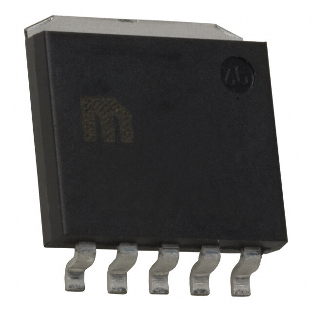
| 产品图片 |
|
| rohs | 符合RoHS无铅 / 符合限制有害物质指令(RoHS)规范要求 |
| 产品系列 | 电源管理 IC,线性稳压器,ON Semiconductor NCP4640H033T1G- |
| 数据手册 | |
| 产品型号 | NCP4640H033T1G |
| PSRR/纹波抑制—典型值 | 30 dB |
| 产品种类 | 线性稳压器 |
| 供应商器件封装 | SOT-89-5 |
| 其它名称 | NCP4640H033T1G-ND |
| 包装 | 带卷 (TR) |
| 商标 | ON Semiconductor |
| 安装类型 | 表面贴装 |
| 安装风格 | SMD/SMT |
| 封装 | Reel |
| 封装/外壳 | SOT-89-5/6 |
| 封装/箱体 | SOT-89-5 |
| 工作温度 | -40°C ~ 150°C |
| 工厂包装数量 | 1000 |
| 最大功率耗散 | 900 mW |
| 最大工作温度 | + 125 C |
| 最大输入电压 | 36 V |
| 最小工作温度 | - 40 C |
| 最小输入电压 | 4 V |
| 极性 | Positive |
| 标准包装 | 1,000 |
| 电压-跌落(典型值) | - |
| 电压-输入 | 4 V ~ 36 V |
| 电压-输出 | 3.3V |
| 电流-输出 | 50mA |
| 电流-限制(最小值) | - |
| 稳压器拓扑 | 正,固定式 |
| 稳压器数 | 1 |
| 系列 | NCP4640 |
| 线路调整率 | 0.5 % / V |
| 负载调节 | 20 mV |
| 输出电压 | 3.3 V |
| 输出电流 | 0.05 A |
| 输出端数量 | 1 |
| 输出类型 | Fixed |


PDF Datasheet 数据手册内容提取
NCP4640 50 mA, Wide Input Range, Voltage Regulator The NCP4640 is a CMOS 50 mA linear voltage regulator with high input voltage and ultra−low supply current. It incorporates multiple protection features such as peak current limit, short circuit current limit and thermal shutdown to ensure a very robust device. http://onsemi.com A high maximum input voltage tolerance of 50 V and a wide MARKING temperature range make the NCP4640 suitable for a variety of DIAGRAMS demanding applications. Features • Operating Input Voltage Range: 4 V to 36 V XXX • XMM Output Voltage Range: 2.0 to 12.0 V (0.1 steps) SOIC6−TL • ±2% Output Voltage Accuracy CASE 751BR 1 • Output Current: min 50 mA (V = 8 V, V = 5 V) IN OUT • Line Regulation: 0.05%/V • Peak Current Limit Circuit 1 • Short Current Limit Circuit XXX • Thermal Shutdown Circuit XMM • Available in SOT−89−5 and SOIC6−TLPackage SOT−89 5 • CASE 528AB These are Pb−Free Devices Typical Applications • XXXX = Specific Device Code Power source for home appliances MM = Date Code • Power source for car audio equipment, navigation system • (Note: Microdot may be in either location) Power source for notebooks, digital TVs, cordless phones and private LAN systems • Power source for office equipment machines such as copiers, ORDERING INFORMATION See detailed ordering and shipping information in the package printers, facsimiles, scanners, projectors, etc. dimensions section on page 15 of this data sheet. NCP4640x VIN VOUT VIN VOUT C1 CE C2 100n GND 100n Figure 1. Typical Application Schematic © Semiconductor Components Industries, LLC, 2011 1 Publication Order Number: February, 2011 − Rev. 1 NCP4640/D
NCP4640 VIN VOUT Internal VR Vref Current Limit Short Protection CE Thermal Shutdown GND Figure 2. Simplified Schematic Block Diagram PIN FUNCTION DESCRIPTION Pin No. Pin No. SOT89 SOIC6−TL Pin Name Description 5 6 VIN Input pin 2 2 GND Ground pin, all ground pins must be connected together when it is mounted on board 4 4 GND Ground pin, all ground pins must be connected together when it is mounted on board − 5 GND Ground pin, all ground pins must be connected together when it is mounted on board 3 3 CE Chip enable pin (“H” active) 1 1 VOUT Output pin http://onsemi.com 2
NCP4640 ABSOLUTE MAXIMUM RATINGS Rating Symbol Value Unit Input Voltage V −0.3 to 50 V IN Peak Input Voltage (Note 1) V 60 V IN Output Voltage VOUT −0.3 to VIN + 0.3 ≤ 50 V Chip Enable Input VCE −0.3 to VIN + 0.3 ≤ 50 V Output Current IOUT 150 mA Power Dissipation SOT−89 PD 900 mW Power Dissipation SOIC6−TL 1700 Junction Temperature T −40 to 150 °C J Storage Temperature T −55 to 125 °C STG ESD Capability, Human Body Model (Note 2) ESD 2000 V HBM ESD Capability, Machine Model (Note 2) ESD 200 V MM Stresses exceeding Maximum Ratings may damage the device. Maximum Ratings are stress ratings only. Functional operation above the Recommended Operating Conditions is not implied. Extended exposure to stresses above the Recommended Operating Conditions may affect device reliability. 1. Duration time = 200 ms 2. This device series incorporates ESD protection and is tested by the following methods: ESD Human Body Model tested per AEC−Q100−002 (EIA/JESD22−A114) ESD Machine Model tested per AEC−Q100−003 (EIA/JESD22−A115) Latchup Current Maximum Rating tested per JEDEC standard: JESD78. THERMAL CHARACTERISTICS Rating Symbol Value Unit Thermal Characteristics, SOT−89 R(cid:2)JA 111 °C/W Thermal Resistance, Junction−to−Air Thermal Characteristics, SOIC6−TL R(cid:2)JA 59 °C/W Thermal Resistance, Junction−to−Air http://onsemi.com 3
NCP4640 ELECTRICAL CHARACTERISTICS TA = 25°C Parameter Test Conditions Symbol Min Typ Max Unit Operating Input Voltage VIN 4 36 V Output Voltage VIN = VOUT + 3 V, IOUT = 1 mA VOUT x0.98 x1.02 V Output Voltage Temp. VIN = VOUT + 3 V, IOUT = 1 mA, TA = −40 to ±100 ppm/°C Coefficient 105°C Line Regulation VIN = VOUT + 1.5 V to 36 V, IOUT = 1 mA LineReg 0.05 0.20 %/V Load Regulation VIN = VOUT + 3 V, 2.0 V ≤ VOUT < 5.0 V LoadReg 10 25 mV IOUT = 1 mA to 40 mA 5.0 V ≤ VOUT < 12.0 V 20 35 Dropout Voltage IOUT = 20 mA 2.0 V ≤ VOUT < 3.7 V VDO (Note 3) V 3.7 V ≤ VOUT < 4.0 V 0.35 0.60 4.0 V ≤ VOUT < 5.0 V 0.25 0.40 5.0 V ≤ VOUT < 12.0 V 0.20 0.35 Output Current VIN = VOUT + 3 V IOUT 50 mA Short Current Limit VOUT = 0 V ISC 50 mA Quiescent Current VIN = VOUT + 3 V, IOUT = 0 mA IQ 9 20 (cid:3)A Standby Current VIN = 36 V, VCE = 0 V ISTB 0.1 1 (cid:3)A CE Pin Threshold Voltage CE Input Voltage “H” VCEH 1.5 VIN V CE Input Voltage “L” VCEL 0 0.3 Thermal Shutdown Temperature TSD 150 °C Thermal Shutdown Release TSR 125 °C Temperature Power Supply Rejection Ratio VIN = 5.0 V, VOUT = 2.0 V, ΔVIN PK−PK = 0.2 V, PSRR 30 dB IOUT = 30 mA, f = 1 kHz Output Noise Voltage VOUT = 2.0 V, IOUT = 30 mA, f = 10 Hz to VN 80 (cid:3)Vrms 100 kHz 3. Dropout voltage for 2.0 V ≤ VOUT < 3.7 V can be computed by this formula: VDO = 4 V − VOUTSET http://onsemi.com 4
NCP4640 TYPICAL CHARACTERISTICS 2.5 3.5 5.0 V 3.0 6.0 V 2.0 4.5 V V) 1.5 VIN = 4.0 V 55..50 VV V) 22..05 VIN = 6.5 V 5.5 V (T (T U U O O 1.5 V 1.0 V 1.0 0.5 0.5 0.0 0.0 0 50 100 150 200 0 50 100 150 200 IOUT (mA) IOUT (mA) Figure 3. Output Voltage vs. Output Current Figure 4. Output Voltage vs. Output Current 2.0 V Version (T = 25(cid:2)C) 3.3 V Version (T = 25(cid:2)C) J J 9.0 14.0 8.0 10.5 V 12.0 14.5 V 11 V 7.0 15 V 10.0 6.0 11.5 V 15.5 V (V)T 5.0 10 V (V)T 8.0 14 V U U O 4.0 O 6.0 V V 3.0 4.0 2.0 2.0 1.0 0.0 0.0 0 50 100 150 200 0 50 100 150 200 IOUT (mA) IOUT (mA) Figure 5. Output Voltage vs. Output Current Figure 6. Output Voltage vs. Output Current 8.0 V Version (T = 25(cid:2)C) 12 V Version (T = 25(cid:2)C) J J 1.50 1.50 1.25 1.25 1.00 1.00 V) V) (O0.75 (O 0.75 D D V V 0.50 0.50 0.25 TJ = 25°C 105°C 0.25 TJ = 25°C 105°C −40°C −40°C 0.00 0.00 0 10 20 30 40 50 0 10 20 30 40 50 IOUT (mA) IOUT (mA) Figure 7. Dropout Voltage vs. Output Current Figure 8. Dropout Voltage vs. Output Current 8.0 V Version 12 V Version http://onsemi.com 5
NCP4640 TYPICAL CHARACTERISTICS 2.10 3.40 2.08 VIN = 5.0 V 3.38 VIN = 6.3 V 2.06 3.36 2.04 3.34 V) 2.02 V) 3.32 (T 2.00 (T 3.30 U U O O V 1.98 V 3.28 1.96 3.26 1.94 3.24 1.92 3.22 1.90 3.20 −40 −20 0 20 40 60 80 100 −40 −20 0 20 40 60 80 100 TJ, JUNCTION TEMPERATURE (°C) TJ, JUNCTION TEMPERATURE (°C) Figure 9. Output Voltage vs. Temperature, Figure 10. Output Voltage vs. Temperature, 2.0 V Version 3.3 V Version 8.20 12.20 8.15 VIN = 11 V 12.15 VIN = 15 V 8.10 12.10 8.05 12.05 V) V) (T 8.00 (T12.00 U U O O V V 7.95 11.95 7.90 11.90 7.85 11.85 7.80 11.80 −40 −20 0 20 40 60 80 100 −40 −20 0 20 40 60 80 100 TJ, JUNCTION TEMPERATURE (°C) TJ, JUNCTION TEMPERATURE (°C) Figure 11. Output Voltage vs. Temperature, Figure 12. Output Voltage vs. Temperature, 8.0 V Version 12 V Version 14 16 12 V 12 8.0 V 14 8.0 V 12 12 V 10 10 (cid:3)A) 8 VOUT = 2.0 V (cid:3)A) (D 3.3 V (D 8 GN 6 GN 3.3 V VOUT = 2.0 V I I 6 4 4 2 2 0 0 −40 −20 0 20 40 60 80 100 0 5 10 15 20 25 30 35 TJ, JUNCTION TEMPERATURE (°C) TJ, JUNCTION TEMPERATURE (°C) Figure 13. Supply Current vs. Temperature Figure 14. Supply Current vs. Input Voltage http://onsemi.com 6
NCP4640 TYPICAL CHARACTERISTICS 2.5 3.5 3.0 2.0 2.5 1 mA 1 mA V) 1.5 V) 2.0 (UT (UT 20 mA O 20 mA O 1.5 V 1.0 V 1.0 0.5 IOUT = 40 mA IOUT = 40 mA 0.5 0.0 0.0 0 5 10 15 20 25 30 35 0 5 10 15 20 25 30 35 VIN, INPUT VOLTAGE (V) VIN, INPUT VOLTAGE (V) Figure 15. Output Voltage vs. Input Voltage, Figure 16. Output Voltage vs. Input Voltage, 2.0 V Version 3.3 V Version 9.0 14.0 8.0 12.0 7.0 10.0 6.0 1 mA V) 5.0 V) 8.0 1 mA (T (T U U O4.0 O 6.0 V V 3.0 20 mA 4.0 20 mA 2.0 IOUT = 40 mA 2.0 1.0 IOUT = 40 mA 0.0 0.0 0 5 10 15 20 25 30 35 0 5 10 15 20 25 30 35 VIN, INPUT VOLTAGE (V) VIN, INPUT VOLTAGE (V) Figure 17. Output Voltage vs. Input Voltage, Figure 18. Output Voltage vs. Input Voltage, 8.0 V Version 12 V Version 100 100 90 90 80 80 70 70 B) 60 B) 60 d d R ( 50 R ( 50 R R S 40 S 40 P 30 IOUT = 1 mA P 30 IOUT = 1 mA 10 mA 10 mA 20 20 10 30 mA 10 30 mA 0 0 0.01 0.1 1 10 100 1000 0.01 0.1 1 10 100 1000 FREQUENCY (kHz) FREQUENCY (kHz) Figure 19. PSRR, 2.0 V Version, V = 5.0 V Figure 20. PSRR, 3.3 V Version, V = 6.3 V IN IN http://onsemi.com 7
NCP4640 TYPICAL CHARACTERISTICS 100 5 90 80 4 70 z) R (dB) 5600 √/Hms 3 R Vr PS 40 IOUT = 1 mA (cid:3)V (N 2 30 10 mA 20 1 10 30 mA 0 0 0.01 0.1 1 10 100 1000 0.01 0.1 1 10 100 1000 FREQUENCY (kHz) FREQUENCY (kHz) Figure 21. PSRR, 3.3 V Version, V = 6.3 V Figure 22. Output Voltage Noise, 2.0 V Version, IN V = 5.0 V, I = 30 mA IN OUT 12 45 40 10 35 z) 8 z) 30 H H √/s √/s25 m 6 m Vr Vr20 (cid:3) (cid:3) V (N 4 V (N15 10 2 5 0 0 0.01 0.1 1 10 100 1000 0.01 0.1 1 10 100 1000 FREQUENCY (kHz) FREQUENCY (kHz) Figure 23. Output Voltage Noise, 3.3 V Version, Figure 24. Output Voltage Noise, 8.0 V Version, V = 6.3 V, I = 30 mA V = 11.0 V, I = 30 mA IN OUT IN OUT 70 60 50 z) H √ 40 /s m Vr (cid:3) 30 (N V 20 10 0 0.01 0.1 1 10 100 1000 FREQUENCY (kHz) Figure 25. Output Voltage Noise, 12.0 V Version, V = 15.0 V, I = 30 mA IN OUT http://onsemi.com 8
NCP4640 TYPICAL CHARACTERISTICS 6.5 6.0 5.5 5.0 (V)UT 2.10 (V)N O VI V 2.05 2.00 1.95 1.90 0 0.2 0.4 0.6 0.8 1.0 1.2 1.4 1.6 1.8 2.0 t ((cid:3)s) Figure 26. Line Transients, 2.0 V Version, t = t = 50 (cid:2)s, I = 1 mA R F OUT 8.0 7.5 7.0 6.5 (V)UT 3.5 6.0 (V)N O VI V 3.4 3.3 3.2 3.1 0 0.2 0.4 0.6 0.8 1.0 1.2 1.4 1.6 1.8 2.0 t ((cid:3)s) Figure 27. Line Transients, 3.3 V Version, t = t = 50 (cid:2)s, I = 1 mA R F OUT 12.5 12.0 11.5 11.0 (V)UT 8.4 (V)N O VI V 8.2 8.0 7.8 7.6 0 0.2 0.4 0.6 0.8 1.0 1.2 1.4 1.6 1.8 2.0 t ((cid:3)s) Figure 28. Line Transients, 8.0 V Version, t = t = 50 (cid:2)s, I = 1 mA R F OUT http://onsemi.com 9
NCP4640 TYPICAL CHARACTERISTICS 16.5 16.0 15.5 15.0 (V)UT12.4 (V)N O VI V 12.2 12.0 11.8 11.6 0 0.2 0.4 0.6 0.8 1.0 1.2 1.4 1.6 1.8 2.0 t ((cid:3)s) Figure 29. Line Transients, 12.0 V Version, t = t = 50 (cid:2)s, I = 1 mA R F OUT 30 20 10 0 V) A) (UT 2.2 (mT O U V 2.1 O I 2.0 1.9 1.8 1.7 0 0.2 0.4 0.6 0.8 1.0 1.2 1.4 1.6 1.8 2.0 t (ms) Figure 30. Load Transients, 2.0 V Version, I = 1 – 20 mA, t = t = 50 (cid:2)s, V = 5.0 V OUT R F IN 30 20 10 0 V) A) (UT 3.7 (mT O U V 3.5 O I 3.3 3.1 2.9 2.7 0 0.2 0.4 0.6 0.8 1.0 1.2 1.4 1.6 1.8 2.0 t (ms) Figure 31. Load Transients, 3.3 V Version, I = 1 – 20 mA, t = t = 50 (cid:2)s, V = 6.3 V OUT R F IN http://onsemi.com 10
NCP4640 TYPICAL CHARACTERISTICS 30 20 10 8.6 0 V) 8.4 A) (UT 8.2 (mT O U V 8.0 O I 7.8 7.6 7.4 7.2 0 0.2 0.4 0.6 0.8 1.0 1.2 1.4 1.6 1.8 2.0 t (ms) Figure 32. Load Transients, 8.0 V Version, I = 1 – 20 mA, t = t = 50 (cid:2)s, V = 11.0 V OUT R F IN 30 20 10 0 V) A) (UT 12.8 (mT O U V 12.4 O I 12.0 11.6 11.2 10.8 0 0.2 0.4 0.6 0.8 1.0 1.2 1.4 1.6 1.8 2.0 t (ms) Figure 33. Load Transients, 12.0 V Version, I = 1 – 20 mA, t = t = 50 (cid:2)s, V = 15.0 V OUT R F IN 60 50 40 30 V) 20A) (UT 2.2 (mT O U V 2.1 O I 2.0 1.9 1.8 1.7 0 0.2 0.4 0.6 0.8 1.0 1.2 1.4 1.6 1.8 2.0 t (ms) Figure 34. Load Transients, 2.0 V Version, I = 20 – 50 mA, t = t = 50 (cid:2)s, V = 5.0 V OUT R F IN http://onsemi.com 11
NCP4640 TYPICAL CHARACTERISTICS 60 50 40 30 V) A) (UT 3.7 (mT VO 3.5 OU I 3.3 3.1 2.9 2.7 0 0.2 0.4 0.6 0.8 1.0 1.2 1.4 1.6 1.8 2.0 t (ms) Figure 35. Load Transients, 3.3 V Version, I = 20 – 50 mA, t = t = 50 (cid:2)s, V = 6.3 V OUT R F IN 60 50 40 30 V) 20A) (UT 8.4 (mT O U V 8.2 O I 8.0 7.8 7.6 7.4 0 0.2 0.4 0.6 0.8 1.0 1.2 1.4 1.6 1.8 2.0 t (ms) Figure 36. Load Transients, 8.0 V Version, I = 20 – 50 mA, t = t = 50 (cid:2)s, V = 11.0 V OUT R F IN 60 50 40 30 V) 20A) (UT12.8 (mT O U V12.4 O I 12.0 11.6 11.2 10.8 0 0.2 0.4 0.6 0.8 1.0 1.2 1.4 1.6 1.8 2.0 t (ms) Figure 37. Load Transients, 12.0 V Version, I = 20 – 50 mA, t = t = 50 (cid:2)s, V = 15.0 V OUT R F IN http://onsemi.com 12
NCP4640 TYPICAL CHARACTERISTICS 8 Chip Enable 6 4 2 0 V) V) V (OUT 12..50 IOUT = 1 mA IOUT = 20 mA V (CE 1.0 IOUT = 50 mA 0.5 0 −0.5 0 50 100 150 200 250 300 350 400 450 500 t ((cid:3)s) Figure 38. Start−up, 2.0 V Version, V = 5.0 V IN 8 Chip Enable 6 4 2 V) 0 V) V (OUT 34 IOUT = 1 mA IOUT = 20 mA V (CE 2 1 IOUT = 50 mA 0 −1 0 50 100 150 200 250 300 350 400 450 500 t ((cid:3)s) Figure 39. Start−up, 3.3 V Version, V = 6.3 V IN 16 Chip Enable 12 8 4 V) 0 V) V (OUT 68 IOUT = 20 mA V (CE IOUT = 1 mA 4 2 IOUT = 50 mA 0 −2 0 50 100 150 200 250 300 350 400 450 500 t ((cid:3)s) Figure 40. Start−up, 8.0 V Version, V = 11.0 V IN http://onsemi.com 13
NCP4640 TYPICAL CHARACTERISTICS 20 Chip Enable 15 10 5 0 V) V) V (OUT1126 IOUT = 20 mA V (CE 8 IOUT = 1 mA 4 IOUT = 50 mA 0 −4 0 50 100 150 200 250 300 350 400 450 500 t ((cid:3)s) Figure 41. Start−up, 12.0 V Version, V = 15.0 V IN http://onsemi.com 14
NCP4640 APPLICATION INFORMATION A typical application circuit for NCP4640 series is shown connected to CE pin. Do not keep CE pin not connected or in Figure 42. between VCEH and VCEL voltage levels. Otherwise output voltage would be unstable or indefinite and unexpected NCP4640x would flow internally. VIN VOUT VIN VOUT Thermal C1 C2 As a power across the IC increase, it might become CE 100n 100n necessary to provide some thermal relief. The maximum GND power dissipation supported by the device is dependent upon board design and layout. Mounting pad configuration on the PCB, the board material, and also the ambient temperature affect the rate of temperature increase for the part. When the device has good thermal conductivity Figure 42. Typical Application Schematic through the PCB the junction temperature will be relatively low in high power dissipation applications. The IC includes internal thermal shutdown circuit that Input Decoupling Capacitor (C1) stops operation of regulator, if junction temperature is The device is stable without any input capacitance, but if higher than 150°C. After that, when junction temperature input line is long and has high impedance or if more stable decreases below 125°C, the operation of voltage regulator operation is needed, input capacitor C1 should be connected would restart. While high power dissipation condition is, the as close as possible to the IC. Recommended range of input regulator starts and stops repeatedly and protects itself capacitor value is 100 nF to 10 (cid:3)F. against overheating. Output Decoupling Capacitor (C2) PCB layout The NCP4641 can work stable without output capacitor, Pins number 2 and 4 of SOT89−5 package and pins but if faster response and higher stability reserve is needed, number 2, 4 and 5 of SOIC6−TL must be wired to the GND output capacitor should be connected as close as possible to plane while it is mounted on board. Make VIN and GND the device. Recommended range of output capacitance is lines sufficient. If their impedance is high, noise pickup or 100 nF to 10 (cid:3)F. Larger values of output capacitance and unstable operation may result. Connect capacitors C1 and lower ESR improves dynamic parameters. C2 as close as possible to the IC, and make wiring as short as possible. Enable Operation The enable pin CE may be used for turning the regulator on and off. The device is activated when high level is ORDERING INFORMATION Nominal Output Device Voltage Description Marking Package Shipping† NCP4640H020T1G 2.0 V Enable High N020 SOT89−5 1000 / Tape & Reel (Pb−Free) NCP4640H030T1G 3.0 V Enable High N030 SOT89−5 1000 / Tape & Reel (Pb−Free) NCP4640H033T1G 3.3 V Enable High N033 SOT89−5 1000 / Tape & Reel (Pb−Free) NCP4640H080T1G 8.0 V Enable High N080 SOT89−5 1000 / Tape & Reel (Pb−Free) NCP4640H120T1G 12.0 V Enable High N120 SOT89−5 1000 / Tape & Reel (Pb−Free) †For information on tape and reel specifications, including part orientation and tape sizes, please refer to our Tape and Reel Packaging Specifications Brochure, BRD8011/D. *To order other package and voltage variants, please contact your ON Semiconductor sales representative. http://onsemi.com 15
NCP4640 PACKAGE DIMENSIONS SOIC6 (HSOP6) CASE 751BR−01 ISSUE O NOTES: D b1 A 1. DIMENSIONING AND TOLERANCING PER ASME F Y14.5M, 1994. 2. CONTROLLING DIMENSION: MILLIMETERS 3. DIMENSION b AND b1 DO NOT INCLUDE DAMBAR 6 4 A3 PROTRUSION. ALLOWAQBLE PROTRUSION SHALL BE 0.10 mm IN EXCESS OF MAXIMUM MATERIAL H E CONDITION. 4. DIMENSIONS D AND E DO NOT INCLUDE MOLD FLASH, PROTRUSIONS, OR GATE BURRS. MOLD 1 3 L2 L C SEATING FNLOATS EHX, CPEREODT R0U.1S5I OmNmS P, EORR SGIADTEE. DBIUMRERNSS ISOHNASL DL 4Xb DETAIL A PLANE 5. ADNATDU EM ASR AE A DNEDT EBR AMRIEN EDDE TAETR DMAITNUEMD FA.T DATUM F. B 0.12 M C A-B D 6. A1 IS DEFINED AS THE VERTICAL DISTANCE FROM THE SEATING PLANE TO THE LOWEST POINT ON THE PACKAGE BODY. MILLIMETERS D 6X DIM MIN MAX 0.10 C A 1.45 1.85 A1 0.05 0.25 A3 0.19 0.30 b 0.30 0.50 b1 1.57 1.77 A1 A e C PSLEAANTIENG DETAIL A ED 43..7720 54..3120 e 3.81 BSC H 5.70 6.30 RECOMMENDED L 0.40 0.60 L2 0.25 BSC SOLDERING FOOTPRINT* 3.81 PITCH 6X 1.05 6.40 1 2X1.87 4X 0.60 DIMENSIONS: MILLIMETERS *For additional information on our Pb−Free strategy and soldering details, please download the ON Semiconductor Soldering and Mounting Techniques Reference Manual, SOLDERRM/D. http://onsemi.com 16
NCP4640 PACKAGE DIMENSIONS SOT−89, 5 LEAD CASE 528AB−01 ISSUE O D NOTES: 1. DIMENSIONING AND TOLERANCING PER ASME Y14.5M, 1994. 2. CONTROLLING DIMENSION: MILLIMETERS. 3. LEAD THICKNESS INCLUDES LEAD FINISH. 4. DIMENSIONS D AND E DO NOT INCLUDE MOLD FLASH, PROTRUSIONS, OR GATE BURRS. E H 5. DIMENSIONS L, L2, L3, L4, L5, AND H ARE MEAS- URED AT DATUM PLANE C. MILLIMETERS DIM MIN MAX 1 A 1.40 1.60 b 0.32 0.52 b1 0.37 0.57 TOP VIEW c 0.30 0.50 D 4.40 4.60 D2 1.40 1.80 E 2.40 2.60 c e 1.40 1.60 A H 4.25 4.45 L 1.10 1.50 0.10 C L2 0.80 1.20 L3 0.95 1.35 C SIDE VIEW L4 0.65 1.05 L5 0.20 0.60 e e RECOMMENDED b1 b L2 MOUNTING FOOTPRINT* L 1 2 3 4X0.57 1.75 1.50 L5 0.45 2.79 5 4 4.65 L3 L4 D2 1.65 BOTTOM VIEW 1.30 1 2X 0.62 2X1.50 DIMENSIONS: MILLIMETERS *For additional information on our Pb−Free strategy and soldering details, please download the ON Semiconductor Soldering and Mounting Techniques Reference Manual, SOLDERRM/D. ON Semiconductor and are registered trademarks of Semiconductor Components Industries, LLC (SCILLC). SCILLC reserves the right to make changes without further notice to any products herein. SCILLC makes no warranty, representation or guarantee regarding the suitability of its products for any particular purpose, nor does SCILLC assume any liability arising out of the application or use of any product or circuit, and specifically disclaims any and all liability, including without limitation special, consequential or incidental damages. “Typical” parameters which may be provided in SCILLC data sheets and/or specifications can and do vary in different applications and actual performance may vary over time. All operating parameters, including “Typicals” must be validated for each customer application by customer’s technical experts. SCILLC does not convey any license under its patent rights nor the rights of others. SCILLC products are not designed, intended, or authorized for use as components in systems intended for surgical implant into the body, or other applications intended to support or sustain life, or for any other application in which the failure of the SCILLC product could create a situation where personal injury or death may occur. Should Buyer purchase or use SCILLC products for any such unintended or unauthorized application, Buyer shall indemnify and hold SCILLC and its officers, employees, subsidiaries, affiliates, and distributors harmless against all claims, costs, damages, and expenses, and reasonable attorney fees arising out of, directly or indirectly, any claim of personal injury or death associated with such unintended or unauthorized use, even if such claim alleges that SCILLC was negligent regarding the design or manufacture of the part. SCILLC is an Equal Opportunity/Affirmative Action Employer. This literature is subject to all applicable copyright laws and is not for resale in any manner. PUBLICATION ORDERING INFORMATION LITERATURE FULFILLMENT: N. American Technical Support: 800−282−9855 Toll Free ON Semiconductor Website: www.onsemi.com Literature Distribution Center for ON Semiconductor USA/Canada P.O. Box 5163, Denver, Colorado 80217 USA Europe, Middle East and Africa Technical Support: Order Literature: http://www.onsemi.com/orderlit Phone: 303−675−2175 or 800−344−3860 Toll Free USA/Canada Phone: 421 33 790 2910 Fax: 303−675−2176 or 800−344−3867 Toll Free USA/Canada Japan Customer Focus Center For additional information, please contact your local Email: orderlit@onsemi.com Phone: 81−3−5773−3850 Sales Representative http://onsemi.com NCP4640/D 17