ICGOO在线商城 > NCP4586DSQ12T1G
 Datasheet下载
- 型号: NCP4586DSQ12T1G
- 制造商: ON Semiconductor
- 库位|库存: xxxx|xxxx
- 要求:
| 数量阶梯 | 香港交货 | 国内含税 |
| +xxxx | $xxxx | ¥xxxx |
查看当月历史价格
查看今年历史价格
NCP4586DSQ12T1G产品简介:
ICGOO电子元器件商城为您提供NCP4586DSQ12T1G由ON Semiconductor设计生产,在icgoo商城现货销售,并且可以通过原厂、代理商等渠道进行代购。 提供NCP4586DSQ12T1G价格参考以及ON SemiconductorNCP4586DSQ12T1G封装/规格参数等产品信息。 你可以下载NCP4586DSQ12T1G参考资料、Datasheet数据手册功能说明书, 资料中有NCP4586DSQ12T1G详细功能的应用电路图电压和使用方法及教程。
| 参数 | 数值 |
| 产品目录 | 集成电路 (IC)半导体 |
| 描述 | IC REG LDO 1.2V 0.15A SC82AB低压差稳压器 |
| 产品分类 | |
| 品牌 | ON Semiconductor |
| 产品手册 | |
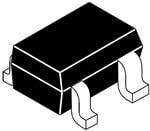
| 产品图片 |
|
| rohs | 符合RoHS无铅 / 符合限制有害物质指令(RoHS)规范要求 |
| 产品系列 | 电源管理 IC,低压差稳压器,ON Semiconductor NCP4586DSQ12T1G- |
| 数据手册 | |
| 产品型号 | NCP4586DSQ12T1G |
| 产品种类 | 低压差稳压器 |
| 供应商器件封装 | SC-82AB |
| 包装 | 带卷 (TR) |
| 商标 | ON Semiconductor |
| 回动电压—最大值 | 1 V |
| 安装类型 | 表面贴装 |
| 安装风格 | SMD/SMT |
| 封装 | Reel |
| 封装/外壳 | SC-82A,SOT-343 |
| 封装/箱体 | SC-82 AB |
| 工作温度 | -40°C ~ 85°C |
| 工厂包装数量 | 3000 |
| 最大功率耗散 | 380 mW |
| 最大工作温度 | + 85 C |
| 最大输入电压 | 7 V |
| 最小工作温度 | - 40 C |
| 标准包装 | 3,000 |
| 电压-跌落(典型值) | 0.67V @ 150mA |
| 电压-输入 | 最高 6.5V |
| 电压-输出 | 1.2V |
| 电压调节准确度 | 1 % |
| 电流-输出 | 150mA |
| 电流-限制(最小值) | - |
| 稳压器拓扑 | 正,固定式 |
| 稳压器数 | 1 |
| 系列 | NCP4586 |
| 负载调节 | 10 mV |
| 输出电压 | 1.2 V |
| 输出电流 | 150 mA |
| 输出端数量 | 1 Output |
| 输出类型 | Adjustable |


- 商务部:美国ITC正式对集成电路等产品启动337调查
- 曝三星4nm工艺存在良率问题 高通将骁龙8 Gen1或转产台积电
- 太阳诱电将投资9.5亿元在常州建新厂生产MLCC 预计2023年完工
- 英特尔发布欧洲新工厂建设计划 深化IDM 2.0 战略
- 台积电先进制程称霸业界 有大客户加持明年业绩稳了
- 达到5530亿美元!SIA预计今年全球半导体销售额将创下新高
- 英特尔拟将自动驾驶子公司Mobileye上市 估值或超500亿美元
- 三星加码芯片和SET,合并消费电子和移动部门,撤换高东真等 CEO
- 三星电子宣布重大人事变动 还合并消费电子和移动部门
- 海关总署:前11个月进口集成电路产品价值2.52万亿元 增长14.8%


PDF Datasheet 数据手册内容提取
NCP4586 150 mA, Low Noise, Low Dropout Regulator The NCP4586 is a CMOS 150 mA low dropout linear with low noise, high ripple rejection, low dropout, high output voltage accuracy and low supply current. The device is available in three configurations: enable high, enable low and enable high plus http://onsemi.com auto−discharge. Small packages allow mounting on high density MARKING PCBs. This is an excellent general purpose regulator, well suited to DIAGRAMS many applications. Features 1 XX • Operating Input Voltage Range: 1.7 V to 6.5 V UDFN4 MM • Output Voltage Range: 1.2 to 5.0 V (available in 0.1 V steps) CASE 517BR 1 • Very Low Dropout: 320 mV Typ. at 150 mA • ±1% Output Voltage Accuracy (V > 2 V, T = 25°C) OUT J • High PSRR: 80 dB at 1 kHz XX • MM Current Fold Back Protection • Stable with a 0.47 (cid:2)F Ceramic Capacitors SC−82AB 1 • CASE 419C Available in 1.0 x 1.0 UDFN, SC−82AB and SOT23−5 Package • These are Pb−Free Devices XXXMM Typical Applications • Battery Powered Equipment SOT−23−5 1 • Portable Communication Equipment CASE 1212 • Cameras, MP3 Players and Camcorder • High Stability Voltage Reference XX, XXX= Specific Product Code MM = Lot Number NCP4586x VIN VOUT VIN VOUT ORDERING INFORMATION C1 C2 CE 470n 470n See detailed ordering and shipping information in the package GND dimensions section on page 15 of this data sheet. Figure 1. Typical Application Schematic © Semiconductor Components Industries, LLC, 2012 1 Publication Order Number: February, 2012 − Rev. 5 NCP4586/D
NCP4586 NCP4586Lxxxxxxxx NCP4586Hxxxxxxxx VIN VOUT VIN VOUT Vref Vref Current Limit Current Limit CE CE GND GND NCP4586Dxxxxxxxx VIN VOUT Vref Current Limit CE GND Figure 2. Simplified Schematic Block Diagram PIN FUNCTION DESCRIPTION Pin No. Pin No. Pin No. UDFN4 SC82−AB SOT23−5 Pin Name Description 4 4 1 VIN Input pin 2 2 2 GND Ground 3 1 3 CE/CE Chip enable pin (“L” active / “H” active) 1 3 5 VOUT Output pin − − 4 NC No connection http://onsemi.com 2
NCP4586 ABSOLUTE MAXIMUM RATINGS Rating Symbol Value Unit Input Voltage (Note 1) V 7 V IN Output Voltage VOUT −0.3 to VIN + 0.3 V Chip Enable Input VCE −0.3 to 7 V Output Current IOUT 200 mA Power Dissipation UDFN4 PD 400 Power Dissipation SC−82AB 380 mW Power Dissipation SOT23−5 420 Maximum Junction Temperature TJ(MAX) +150 °C Operating Ambient Temperature TA −40 to +85 °C Storage Temperature TSTG −55 to +125 °C ESD Capability, Human Body Model (Note 2) ESDHBM 2000 V ESD Capability, Machine Model (Note 2) ESDMM 200 V Stresses exceeding Maximum Ratings may damage the device. Maximum Ratings are stress ratings only. Functional operation above the Recommended Operating Conditions is not implied. Extended exposure to stresses above the Recommended Operating Conditions may affect device reliability. 1. Refer to ELECTRICAL CHARACTERISTIS and APPLICATION INFORMATION for Safe Operating Area. 2. This device series incorporates ESD protection and is tested by the following methods: ESD Human Body Model tested per AEC−Q100−002 (EIA/JESD22−A114) ESD Machine Model tested per AEC−Q100−003 (EIA/JESD22−A115) Latchup Current Maximum Rating tested per JEDEC standard: JESD78. THERMAL CHARACTERISTICS Rating Symbol Value Unit Thermal Characteristics, UDFN4 R(cid:3)JA 250 °C/W Thermal Resistance, Junction−to−Air Thermal Characteristics, SOT23−5 R(cid:3)JA 238 °C/W Thermal Resistance, Junction−to−Air Thermal Characteristics, SC 82AB R(cid:3)JA 263 °C/W Thermal Resistance, Junction−to−Air http://onsemi.com 3
NCP4586 ELECTRICAL CHARACTERISTICS −40°C ≤ TA ≤ 85°C; VIN = VOUT(NOM) + 1 V or 2.5 V, whichever is greater; IOUT = 1 mA, CIN = COUT = 0.47 (cid:2)F, unless otherwise noted. Typical values are at TA = +25 °C. Parameter Test Conditions Symbol Min Typ Max Unit Operating Input Voltage VIN 1.7 6.5 V Output Voltage TA = +25 °C VOUT > 2 V VOUT x0.99 x1.01 V VOUT ≤ 2 V −20 20 mV −40°C ≤ TA ≤ 85°C VOUT > 2 V x0.985 x1.015 V VOUT ≤ 2 V −30 30 mV Output Voltage Temp. Coefficient TA = −40 to 85°C ±20 ppm/°C Line Regulation VIN = VOUT + 0.5 V to 5 V LineReg 0.02 0.10 %/V Load Regulation IOUT = 1 mA to 150 mA LoadReg 10 30 mV Dropout Voltage IOUT = 150 mA 1.2 V ≤ VOUT < 1.5 V VDO 0.67 1.00 V 1.5 V ≤ VOUT < 1.7 V 0.54 0.81 1.7 V ≤ VOUT < 2.0 V 0.46 0.68 2.0 V ≤ VOUT < 2.5 V 0.41 0.60 2.5 V ≤ VOUT < 4.0 V 0.32 0.51 4.0 V ≤ VOUT 0.24 0.37 Output Current IOUT 150 mA Short Current Limit VOUT = 0 V ISC 40 mA Quiescent Current IOUT = 0 mA IQ 38 58 (cid:2)A Standby Current VCE = VIN (L version), VCE = 0 V(H and ISTB 0.1 1 (cid:2)A D version), TA = 25°C CE/CE Pin Threshold Voltage CE / CE Input Voltage “H” VCEH 1.0 V CE / CE Input Voltage “L” VCEL 0.4 CE Pull Down Current H and D version IPD 0.4 (cid:2)A Power Supply Rejection Ratio VIN = VOUT + 1 V or 3.0 V whichever is higher, PSRR 80 dB IOUT = 30 mA, f = 1 kHz Output Noise Voltage VOUT = 1.2 V, IOUT = 30 mA, f = 10 Hz to VN 30 (cid:2)Vrms 100 kHz Low Output N−ch Tr. On D Version only, VIN = 4 V, VCE = 0 V RLOW 30 (cid:4) Resistance http://onsemi.com 4
NCP4586 TYPICAL CHARACTERISTICS 1.4 3.0 4.2 V 1.2 2.5 6.0 V VIN = 2.2 V 3.6 V 1.0 4.2 V 2.0 V) 0.8 6.0 V V) VIN = 6.5 V (T (T1.5 3.8 V U 6.5 V U O 0.6 O V V 1.0 0.4 0.2 0.5 0.0 0.0 0 100 200 300 400 500 0 100 200 300 400 500 IOUT (mA) IOUT (mA) Figure 3. Output Voltage vs. Output Current Figure 4. Output Voltage vs. Output Current 1.2 V Version (T = 25 (cid:2)C) 2.8 V Version (T = 25 (cid:2)C) A A 6 0.8 0.7 5 0.6 6.0 V 4 25°C 0.5 V) VIN = 6.5 V V) (UT 3 (O 0.4 85°C O D V V 0.3 −40°C 2 0.2 1 0.1 0 0 0 100 200 300 400 500 0 100 200 300 400 500 IOUT (mA) IOUT (mA) Figure 5. Output Voltage vs. Output Current Figure 6. Dropout Voltage vs. Output Current 5.0 V version (T = 25(cid:2)C) 1.2 V version A 0.40 0.30 0.35 0.25 0.30 0.20 (V)DO 00..2205 25°C (V)O0.15 25°C V D 85°C 0.15 85°C V 0.10 −40°C 0.10 −40°C 0.05 0.05 0.00 0.00 0 100 200 300 400 500 0 25 50 75 100 125 150 IOUT (mA) IOUT (mA) Figure 7. Dropout Voltage vs. Output Current Figure 8. Dropout Voltage vs. Output Current 2.8 V Version 5.0 V Version http://onsemi.com 5
NCP4586 TYPICAL CHARACTERISTICS 1.25 2.85 VIN = 2.2 V VIN = 3.8 V 1.23 2.83 V) 1.21 V) 2.81 (T (T U U O O V 1.19 V 2.79 1.17 2.77 1.15 2.75 −40 −20 0 20 40 60 80 −40 −20 0 20 40 60 80 TJ, JUNCTION TEMPERATURE (°C) TJ, JUNCTION TEMPERATURE (°C) Figure 9. Output Voltage vs. Temperature, 1.2 V Figure 10. Output Voltage vs. Temperature, Version 2.8 V version 5.05 50.0 5.04 VIN = 6.0 V 45.0 5.03 40.0 5.02 35.0 (V)OUT55..0001 (cid:2) (A)N 2350..00 V 4.99 II 20.0 4.98 15.0 4.97 10.0 4.96 5.0 4.95 0.0 −40 −20 0 20 40 60 80 0 1 2 3 4 5 6 TJ, JUNCTION TEMPERATURE (°C) VIN (V) Figure 11. Output Voltage vs. Temperature, Figure 12. Supply Current vs. Input Voltage, 5.0 V Version 1.2 V Version 50.0 50.0 45.0 45.0 40.0 40.0 35.0 35.0 30.0 30.0 A) A) (cid:2) 25.0 (cid:2) 25.0 (N (N II20.0 II 20.0 15.0 15.0 10.0 10.0 5.0 5.0 0.0 0.0 0 1 2 3 4 5 6 0 1 2 3 4 5 6 VIN (V) VIN (V) Figure 14. Supply Current vs. Input Voltage, Figure 13. Supply Current vs. Input Voltage, 2.8 V Version 5.0 V version http://onsemi.com 6
NCP4586 TYPICAL CHARACTERISTICS 40.0 40.0 39.0 VIN = 2.2 V 39.0 VIN = 3.8 V 38.0 38.0 37.0 37.0 36.0 36.0 A) A) (cid:2) 35.0 (cid:2) 35.0 (N (N II34.0 II 34.0 33.0 33.0 32.0 32.0 31.0 31.0 30.0 30.0 −40 −20 0 20 40 60 80 −40 −20 0 20 40 60 80 TJ, JUNCTION TEMPERATURE (°C) TJ, JUNCTION TEMPERATURE (°C) Figure 15. Supply Current vs. Temperature, Figure 16. Supply Current vs. Temperature, 1.2 V Version 2.8 V Version 45 1.4 44 VIN = 6.0 V 1.2 43 42 1.0 1 mA (cid:2)I (A)IN 344091 V (V)OUT 00..68 30 mA 38 0.4 37 IOUT = 50 mA 0.2 36 35 0.0 −40 −20 0 20 40 60 80 0 1 2 3 4 5 6 7 TJ, JUNCTION TEMPERATURE (°C) VIN (V) Figure 17. Supply Current vs. Temperature, Figure 18. Output Voltage vs. Input Voltage, 5.0 V Version 1.2 V Version 3.0 6.0 2.5 5.0 2.0 4.0 1 mA V) V) (T 1.5 (T 3.0 U U O O V V 1.0 2.0 30 mA 1 mA 0.5 1.0 30 mA IOUT = 50 mA IOUT = 50 mA 0.0 0.0 0 1 2 3 4 5 6 7 0 1 2 3 4 5 6 7 VIN (V) VIN (V) Figure 19. Output Voltage vs. Input Voltage, Figure 20. Output Voltage vs. Input Voltage, 2.8 V Version 5.0 V Version http://onsemi.com 7
NCP4586 TYPICAL CHARACTERISTICS 100 100 90 1 mA 90 1 mA 80 30 mA 80 30 mA 70 70 IOUT = 150 mA B) 60 IOUT = 150 mA B) 60 d d R ( 50 R ( 50 R R PS 40 PS 40 30 30 20 20 10 10 0 0 0.01 0.1 1 10 100 1000 0.01 0.1 1 10 100 1000 FREQUENCY (kHz) FREQUENCY (kHz) Figure 21. PSRR, 1.2 V Version Figure 22. PSRR, 2.8 V Version 100 1.6 90 1.4 80 1 mA 1.2 70 30 mA z) 1.0 RR (dB) 5600 IOUT = 150 mA √V/Hrms0.8 PS 40 (cid:2) (N0.6 30 V 0.4 20 0.2 10 0 0 0.01 0.1 1 10 100 1000 0.01 0.1 1 10 100 1000 FREQUENCY (kHz) FREQUENCY (kHz) Figure 23. PSRR, 5.0 V Version Figure 24. Output Voltage Noise, 1.2 V Version 7.0 7.0 6.0 6.0 5.0 5.0 z) z) H H √/s4.0 √/s4.0 m m Vr Vr (cid:2) 3.0 (cid:2) 3.0 (N (N V V 2.0 2.0 1.0 1.0 0 0 0.01 0.1 1 10 100 1000 0.01 0.1 1 10 100 1000 FREQUENCY (kHz) FREQUENCY (kHz) Figure 25. Output Voltage Noise, 2.8 V Version Figure 26. Output Voltage Noise, 5.0 V Version http://onsemi.com 8
NCP4586 TYPICAL CHARACTERISTICS 4 3 2 (V)UT 1 (V)N O1.205 VI V 1.200 1.195 1.190 0 10 20 30 40 50 60 70 80 90 100 t ((cid:2)s) Figure 27. Line Transients, 1.2 V Version, t = t = 5 (cid:2)s, I = 30 mA R F OUT 6 5 4 (V)UT 3 (V)N O2.805 VI V 2.800 2.795 2.790 0 10 20 30 40 50 60 70 80 90 100 t ((cid:2)s) Figure 28. Line Transients, 2.8 V Version, t = t = 5 (cid:2)s, I = 30 mA R F OUT 7 6 5 (V)UT 4 (V)N O5.005 VI V 5.000 4.995 4.990 0 10 20 30 40 50 60 70 80 90 100 t ((cid:2)s) Figure 29. Line Transients, 5.0 V Version, t = R t = 5 (cid:2)s, I = 30 mA F OUT http://onsemi.com 9
NCP4586 TYPICAL CHARACTERISTICS 200 150 100 50 V) 0 A) (UT (mT O U V 1.23 O I 1.22 1.21 1.20 1.19 1.18 0 10 20 30 40 50 60 70 80 90 100 t ((cid:2)s) Figure 30. Load Transients, 1.2 V Version, I = 50 − 100 mA, t = t = 0.5 (cid:2)s, V = 2.2 V OUT R F IN 200 150 100 50 V) 0 A) (UT (mT O U V 2.83 IO 2.82 2.81 2.80 2.79 2.78 0 10 20 30 40 50 60 70 80 90 100 t ((cid:2)s) Figure 31. Load Transients, 2.8 V Version, I = 50 − 100 mA, t = t = 0.5 (cid:2)s, V = 3.8 V OUT R F IN 200 150 100 50 V) 0 A) (UT (mT O U V 5.03 O I 5.02 5.01 4.99 4.98 0 10 20 30 40 50 60 70 80 90 100 t ((cid:2)s) Figure 32. Load Transients, 5.0 V Version, I = 50 − 100 mA, t = t = 0.5 (cid:2)s, V = 6.0 V OUT R F IN http://onsemi.com 10
NCP4586 TYPICAL CHARACTERISTICS 200 150 100 50 V) A) (UT 0 (mT O U V 1.30 O I 1.25 1.20 1.15 1.10 1.05 0 10 20 30 40 50 60 70 80 90 100 t ((cid:2)s) Figure 33. Load Transients, 1.2 V Version, I = 1 − 150 mA, t = t = 0.5 (cid:2)s, V = 2.2 V OUT R F IN 200 150 100 50 V) A) (UT 0 (mT O U V 2.90 O I 2.85 2.80 2.75 2.70 2.65 0 10 20 30 40 50 60 70 80 90 100 t ((cid:2)s) Figure 34. Load Transients, 2.8 V Version, I = 1 − 150 mA, t = t = 0.5 (cid:2)s, V = 3.8 V OUT R F IN 200 150 100 50 V) A) (UT 0 (mT O U V 5.10 O I 5.05 5.00 4.95 4.90 4.85 0 10 20 30 40 50 60 70 80 90 100 t ((cid:2)s) Figure 35. Load Transients, 5.0 V Version, I = 1 − 150 mA, t = t = 0.5 (cid:2)s, V = 6.0 V OUT R F IN http://onsemi.com 11
NCP4586 TYPICAL CHARACTERISTICS 4 Chip Enable 3 2 1 V) 0 V) V (OUT 21..05 IOUT = 150 mA (VCE 1.0 IOUT = 1 mA 0.5 0.0 −0.5 0 2 4 6 8 10 12 14 16 18 20 t ((cid:2)s) Figure 36. Start−up, 1.2 V Version, V = 2.2 V IN 5 Chip Enable 4 3 2 V) 1 V) V (OUT 43 (VCE 2 IOUT = 1 mA 1 IOUT = 150 mA 0 −1 0 2 4 6 8 10 12 14 16 18 20 t ((cid:2)s) Figure 37. Start−up, 2.8 V Version, V = 3.8 V IN 10 8 Chip Enable 6 4 V) 2 V) V (OUT 86 0 (VCE 4 2 IOUT = 1 mA IOUT = 150 mA 0 −2 0 5 10 15 20 25 30 35 40 45 50 t ((cid:2)s) Figure 38. Start−up, 5.0 V Version, V = 6.0 V IN http://onsemi.com 12
NCP4586 TYPICAL CHARACTERISTICS 4 3 2 1 Chip Enable V) 0 V) V (OUT 21..05 V (CE 1.0 IOUT = 1 mA IOUT = 30 mA 0.5 0.0 IOUT = 150 mA −0.5 0 10 20 30 40 50 60 70 80 90 100 t ((cid:2)s) Figure 39. Shutdown, 1.2 V Version D, V = 2.2 V IN 5 4 3 2 V) Chip Enable V) V (OUT 21..05 1 V (CE 1.0 IOUT = 1 mA 0.5 IOUT = 30 mA 0.0 IOUT = 150 mA −0.5 0 10 20 30 40 50 60 70 80 90 100 t ((cid:2)s) Figure 40. Shutdown, 2.8 V Version D, V = 3.8 V IN 10 8 6 4 V (V)OUT 86 Chip Enable 20 V (V)CE 4 IOUT = 1 mA 2 IOUT = 30 mA 0 IOUT = 150 mA −2 0 10 20 30 40 50 60 70 80 90 100 t ((cid:2)s) Figure 41. Shutdown, 5.0 V version D, V = 6.0 V IN http://onsemi.com 13
NCP4586 APPLICATION INFORMATION A typical application circuit for NCP4586 series is shown version of IC. Active high or low versions are available; in Figure 42. please see the ordering information table. The Enable pin has an internal pull down current source for versions H and NCP4586x D. If the enable function is not needed connect the CE pin to VIN VOUT ground for version L or connect the CE pin to VIN for VIN VOUT versions H and D. C1 C2 CE 470n 470n Output Discharger GND The D version includes a transistor between VOUT and GND that is used for faster discharging of the output capacitor. This function is activated when the IC goes into disable mode. Figure 42. Typical Application Schematic Thermal As power across the IC increases, it might become necessary to provide some thermal relief. The maximum Input Decoupling Capacitor (C1) power dissipation supported by the device is dependent A 470 nF ceramic input decoupling capacitor should be upon board design and layout. Mounting pad configuration connected as close as possible to the input and ground pin of on the PCB, the board material, and also the ambient the NCP4586. Higher values and lower ESR improves line temperature affect the rate of temperature rise for the part. transient response. That is to say, when the device has good thermal conductivity through the PCB, the junction temperature will Output Decoupling Capacitor (C2) be relatively low with high power dissipation applications. A 470 nF or larger ceramic output decoupling capacitor is sufficient to achieve stable operation of the IC. If a tantalum PCB Layout capacitor is used, and its ESR is high, loop oscillation may Make VIN and GND line sufficient. If their impedance is result. The capacitors should be connected as close as high, noise pickup or unstable operation may result. Connect possible to the output and ground pins. Larger values and capacitors C1 and C2 as close as possible to the IC, and make lower ESR improves dynamic parameters. wiring as short as possible. Enable Operation The Enable pin CE or CE may be used for turning the regulator on and off. Control polarity is dependent on http://onsemi.com 14
NCP4586 ORDERING INFORMATION Nominal Output Device Voltage Description Marking Package Shipping† NCP4586DSQ12T1G 1.2 V LA NCP4586DSQ18T1G 1.8 V LG NCP4586DSQ28T1G 2.8 V MH SC82AB 3000 / Tape & Reel NCP4586DSQ30T1G 3.0 V NA (Pb−Free) NCP4586DSQ33T1G 3.3 V ND NCP4586DSQ50T1G 5.0 V QA NCP4586DMU12TCG 1.2 V VA NCP4586DMU14TCG 1.4 V VC NCP4586DMU15TCG 1.5 V VD NCP4586DMU18TCG 1.8 V VG Enable High, UDFN4 NCP4586DMU25TCG 2.5 V VQ 10000 / Tape & Reel Auto discharge (Pb−Free) NCP4586DMU28TCG 2.8 V VT NCP4586DMU30TCG 3.0 V VW NCP4586DMU33TCG 3.3 V VZ NCP4586DMU50TCG 5.0 V WS NCP4586DSN12T1G 1.2 V H2A NCP4586DSN18T1G 1.8 V H2G NCP4586DSN28T1G 2.8 V H2T SOT−23−5 3000 / Tape & Reel NCP4586DSN30T1G 3.0 V H2W (Pb−Free) NCP4586DSN33T1G 3.3 V H2Z NCP4586DSN50T1G 5.0 V J2S †For information on tape and reel specifications, including part orientation and tape sizes, please refer to our Tape and Reel Packaging Specifications Brochure, BRD8011/D. NOTE: To order other package and voltage variants, please contact your ON Semiconductor sales representative. http://onsemi.com 15
NCP4586 PACKAGE DIMENSIONS UDFN4 1.0x1.0, 0.65P CASE 517BR−01 ISSUE O NOTES: D A 4XL3 1. DIMENSIONING AND TOLERANCING PER ASME Y14.5M, 1994. B 2. CONTROLLING DIMENSION: MILLIMETERS. 3. DIMENSION b APPLIES TO PLATED TERMINAL AND IS MEASURED BETWEEN 0.15 AND c 0.18 REFEPRINE ONCNEE ÉÉ L2 typ 4. 0C.O20P LmAmN AFRRIOTMY ATEPRPLMIEINSA TLO. THE EXPOSED E PAD AS WELL AS THE TERMINALS. 2X 0.05 C ÉÉ DETAIL A MILLIMETERS DIM MIN MAX 2X 0.05 C A −−− 0.60 3X0.43 4X0.23 A1 0.00 0.05 TOP VIEW A3 0.10 REF b 0.20 0.30 0.05 C (A3) D 1.00 BSC D2 0.43 0.53 A E 1.00 BSC e 0.65 BSC 0.05 C 3X0.10 L 0.20 0.30 L2 0.27 0.37 NOTE 4 SIDE VIEW A1 C SPELAATNIENG DETAIL B L3 0.02 0.12 RECOMMENDED e MOUNTING FOOTPRINT* e/2 DETAIL A 1 2 3XL PIT0C.6H5 DETAIL B 2X 0.52 D2 D2 PACKAGE OUTLINE 45(cid:2) 4 3 1.30 4Xb 0.05 M C A B BOTTOM VIEW NOTE 3 0.53 4X 0.30 DIMENSIONS: MILLIMETERS *For additional information on our Pb−Free strategy and soldering details, please download the ON Semiconductor Soldering and Mounting Techniques Reference Manual, SOLDERRM/D. http://onsemi.com 16
NCP4586 PACKAGE DIMENSIONS SC−82AB CASE 419C−02 ISSUE E NOTES: 1. DIMENSIONING AND TOLERANCING PER ANSI Y14.5M, 1982. A 2. CONTROLLING DIMENSION: MILLIMETER. 3. 419C−01 OBSOLETE. NEW STANDARD IS G 419C−02. C 4. DIMENSIONS A AND B DO NOT INCLUDE D3 PL N MBUORLRDS F.LASH, PROTRUSIONS, OR GATE MILLIMETERS INCHES 4 3 DIM MIN MAX MIN MAX A 1.8 2.2 0.071 0.087 S B K B 1.15 1.35 0.045 0.053 C 0.8 1.1 0.031 0.043 1 2 D 0.2 0.4 0.008 0.016 F 0.3 0.5 0.012 0.020 G 1.1 1.5 0.043 0.059 F H H 0.0 0.1 0.000 0.004 J J 0.10 0.26 0.004 0.010 L K 0.1 −−− 0.004 −−− 0.05 (0.002) L 0.05 BSC 0.002 BSC N 0.2 REF 0.008 REF S 1.8 2.4 0.07 0.09 SOLDERING FOOTPRINT* 1.30 0.0512 0.65 0.026 1.90 0.075 0.95 0.037 0.90 0.035 (cid:2) (cid:3) 0.70 mm SCALE 10:1 0.028 inches *For additional information on our Pb−Free strategy and soldering details, please download the ON Semiconductor Soldering and Mounting Techniques Reference Manual, SOLDERRM/D. http://onsemi.com 17
NCP4586 PACKAGE DIMENSIONS SOT−23 5−LEAD CASE 1212−01 ISSUE A NOTES: A 1. DIMENSIONING AND TOLERANCING PER ASME Y14.5M, 1994. A D B A2 2. CONTROLLING DIMENSIONS: MILLIMETERS. 0.05 S A1 3. DATUM C IS THE SEATING PLANE. MILLIMETERS 5 4 DIM MIN MAX E L A --- 1.45 1 2 3 A1 0.00 0.10 E1 A2 1.00 1.30 L1 5Xb C b 0.30 0.50 c 0.10 0.25 e 0.10 M C B S A S C D 2.70 3.10 E 2.50 3.10 E1 1.50 1.80 e 0.95 BSC L 0.20 --- L1 0.45 0.75 RECOMMENDED SOLDERING FOOTPRINT* 3.30 5X 0.85 5X 0.56 0.95 PITCH DIMENSIONS: MILLIMETERS *For additional information on our Pb−Free strategy and soldering details, please download the ON Semiconductor Soldering and Mounting Techniques Reference Manual, SOLDERRM/D. ON Semiconductor and are registered trademarks of Semiconductor Components Industries, LLC (SCILLC). SCILLC reserves the right to make changes without further notice to any products herein. SCILLC makes no warranty, representation or guarantee regarding the suitability of its products for any particular purpose, nor does SCILLC assume any liability arising out of the application or use of any product or circuit, and specifically disclaims any and all liability, including without limitation special, consequential or incidental damages. “Typical” parameters which may be provided in SCILLC data sheets and/or specifications can and do vary in different applications and actual performance may vary over time. All operating parameters, including “Typicals” must be validated for each customer application by customer’s technical experts. SCILLC does not convey any license under its patent rights nor the rights of others. SCILLC products are not designed, intended, or authorized for use as components in systems intended for surgical implant into the body, or other applications intended to support or sustain life, or for any other application in which the failure of the SCILLC product could create a situation where personal injury or death may occur. Should Buyer purchase or use SCILLC products for any such unintended or unauthorized application, Buyer shall indemnify and hold SCILLC and its officers, employees, subsidiaries, affiliates, and distributors harmless against all claims, costs, damages, and expenses, and reasonable attorney fees arising out of, directly or indirectly, any claim of personal injury or death associated with such unintended or unauthorized use, even if such claim alleges that SCILLC was negligent regarding the design or manufacture of the part. SCILLC is an Equal Opportunity/Affirmative Action Employer. This literature is subject to all applicable copyright laws and is not for resale in any manner. PUBLICATION ORDERING INFORMATION LITERATURE FULFILLMENT: N. American Technical Support: 800−282−9855 Toll Free ON Semiconductor Website: www.onsemi.com Literature Distribution Center for ON Semiconductor USA/Canada P.O. Box 5163, Denver, Colorado 80217 USA Europe, Middle East and Africa Technical Support: Order Literature: http://www.onsemi.com/orderlit Phone: 303−675−2175 or 800−344−3860 Toll Free USA/Canada Phone: 421 33 790 2910 Fax: 303−675−2176 or 800−344−3867 Toll Free USA/Canada Japan Customer Focus Center For additional information, please contact your local Email: orderlit@onsemi.com Phone: 81−3−5817−1050 Sales Representative http://onsemi.com NCP4586/D 18
Mouser Electronics Authorized Distributor Click to View Pricing, Inventory, Delivery & Lifecycle Information: O N Semiconductor: NCP4586DMU33TCG NCP4586DSN50T1G NCP4586DSN18T1G NCP4586DSN12T1G NCP4586DSN28T1G NCP4586DSN33T1G NCP4586DMU12TCG NCP4586DMU18TCG NCP4586DMU28TCG NCP4586DMU30TCG NCP4586DMU50TCG NCP4586DSQ12T1G NCP4586DSQ18T1G NCP4586DSQ28T1G NCP4586DSQ30T1G NCP4586DSQ33T1G NCP4586DSQ50T1G NCP4586DMU14TCG NCP4586DMU15TCG NCP4586DMU25TCG NCP4586DSN30T1G