ICGOO在线商城 > 电路保护 > TVS - 混合技术 > NCP360SNT1G

 Datasheet下载
- 型号: NCP360SNT1G
- 制造商: ON Semiconductor
- 库位|库存: xxxx|xxxx
- 要求:
| 数量阶梯 | 香港交货 | 国内含税 |
| +xxxx | $xxxx | ¥xxxx |
查看当月历史价格
查看今年历史价格
NCP360SNT1G产品简介:
ICGOO电子元器件商城为您提供NCP360SNT1G由ON Semiconductor设计生产,在icgoo商城现货销售,并且可以通过原厂、代理商等渠道进行代购。 NCP360SNT1G价格参考。ON SemiconductorNCP360SNT1G封装/规格:TVS - 混合技术, 。您可以下载NCP360SNT1G参考资料、Datasheet数据手册功能说明书,资料中有NCP360SNT1G 详细功能的应用电路图电压和使用方法及教程。
| 参数 | 数值 |
| 产品目录 | |
| 描述 | IC CTLR USB POS OVP FET 5TSOP监控电路 USB OVP SUPERVISORY |
| 产品分类 | TVS - 其它复合集成电路 - IC |
| 品牌 | ON Semiconductor |
| 产品手册 | |
| 产品图片 |
|
| rohs | 符合RoHS无铅 / 符合限制有害物质指令(RoHS)规范要求 |
| 产品系列 | 电源管理 IC,监控电路,ON Semiconductor NCP360SNT1G- |
| NumberofInputsMonitored | 1 Input |
| 数据手册 | |
| 产品型号 | NCP360SNT1G |
| 产品目录页面 | |
| 产品种类 | Drivers- MOSFET/IGBT |
| 人工复位 | No Manual Reset |
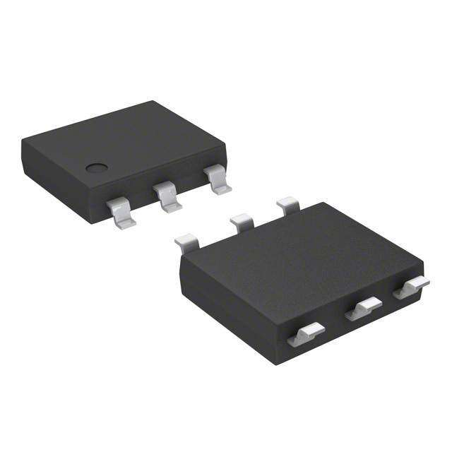
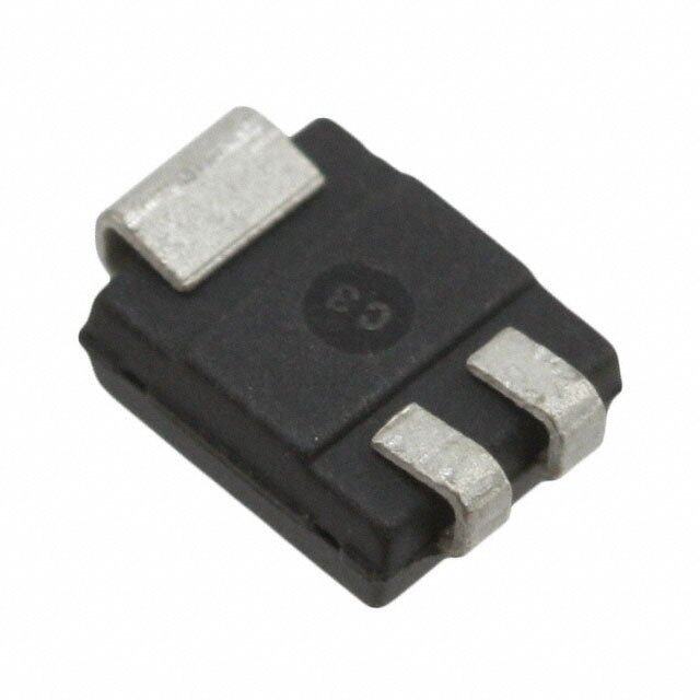
| 供应商器件封装 | 5-TSOP |
| 其它名称 | NCP360SNT1GOSCT |
| 功率(W) | - |
| 包装 | 剪切带 (CT) |
| 商标 | ON Semiconductor |
| 安装风格 | SMD/SMT |
| 封装 | Reel |
| 封装/外壳 | 6-TSOP(0.059",1.50mm 宽)5 引线 |
| 封装/箱体 | TSOP-5 |
| 工厂包装数量 | 3000 |
| 应用 | USB |
| 技术 | 混合技术 |
| 最大工作温度 | + 85 C |
| 最小工作温度 | - 40 C |
| 标准包装 | 1 |
| 电压-工作 | 1.2 ~ 20V |
| 电压-箝位 | 7.4V |
| 电池备用开关 | No Backup |
| 电源电压-最大 | 20 V |
| 电源电压-最小 | 1.2 V |
| 电路数 | 1 |
| 监视器 | No Watchdog |
| 类型 | Voltage Supervisory |
| 系列 | NCP360 |
| 被监测输入数 | 1 Input |
| 阈值电压 | 1.2 V to 20 V |


- 商务部:美国ITC正式对集成电路等产品启动337调查
- 曝三星4nm工艺存在良率问题 高通将骁龙8 Gen1或转产台积电
- 太阳诱电将投资9.5亿元在常州建新厂生产MLCC 预计2023年完工
- 英特尔发布欧洲新工厂建设计划 深化IDM 2.0 战略
- 台积电先进制程称霸业界 有大客户加持明年业绩稳了
- 达到5530亿美元!SIA预计今年全球半导体销售额将创下新高
- 英特尔拟将自动驾驶子公司Mobileye上市 估值或超500亿美元
- 三星加码芯片和SET,合并消费电子和移动部门,撤换高东真等 CEO
- 三星电子宣布重大人事变动 还合并消费电子和移动部门
- 海关总署:前11个月进口集成电路产品价值2.52万亿元 增长14.8%


PDF Datasheet 数据手册内容提取
NCP360, NCV360 USB Positive Overvoltage Protection Controller with Internal PMOS FET and Status FLAG The NCP360 disconnects systems at its output when wrong VBUS http://onsemi.com operating conditions are detected at its input. The system is positive overvoltage protected up to +20V. MARKING DIAGRAMS Thanks to an integrated PMOS FET, no external device is necessary, reducing the system cost and the PCB area of the UDFN6 1 application board. MU SUFFIX xx M (cid:2) The NCP360 is able to instantaneously disconnect the output from CASE 517AB the input if the input voltage exceeds the overvoltage threshold M = Date Code (OVLO). (cid:2) = Pb−Free Package The NCP360 provides a negative going flag (FLAG) output, which alerts the system that a fault has occurred. In addition, the device has ESD−protected input (15kV Air) when TSOP−5 xxxAYW(cid:2) bypassed with a 1(cid:2)F or larger capacitor. 5 SN SUFFIX (cid:2) CASE 483 1 1 Features • Very Fast Protection, Up to 20V, with 25 (cid:2)A Current Consumption A = Assembly Location Y = Year • On−chip PMOS Transistor W = Work Week • Overvoltage Lockout (OVLO) (cid:2) = Pb−Free Package • (Note: Microdot may be in either location) Undervoltage Lockout (UVLO) • Alert FLAG Output • EN Enable Pin ORDERING INFORMATION • Thermal Shutdown See detailed ordering, marking and shipping information in the • Compliance to IEC61000−4−2 (Level 4) package dimensions section on page 11 of this data sheet. 8kV (Contact) 15kV (Air) • ESD Ratings: Machine Model = B ESD Ratings: Human Body Model = 2 • 6 Lead UDFN 2x2 mm Package • 5 Lead TSOP 3x3 mm Package • NCV Prefix for Automotive and Other Applications Requiring Unique Site and Control Change Requirements; AEC−Q100 Qualified and PPAP Capable • These are Pb−Free Devices Applications • USB Devices • Mobile Phones • Peripheral • Personal Digital Applications • MP3 Players Q © Semiconductor Components Industries, LLC, 2012 1 Publication Order Number: March, 2012 − Rev. 10 NCP360/D
NCP360, NCV360 PIN CONNECTIONS EN 1 6 FLAG IN 1 5 OUT GND 2 PAD1 5 OUT GND 2 IN 3 4 OUT EN 3 4 FLAG UDFN6 TSOP−5 (Top Views) PIN FUNCTION DESCRIPTION (cid:2)UDFN6 Package) Pin No. Name Type Description 1 EN INPUT Enable Pin. The device enters in shutdown mode when this pin is tied to a high level. In this case the output is disconnected from the input. To allow normal functionality, the EN pin shall be connected to GND or to a I/O pin. This pin does not have an impact on the fault detection. 2 GND POWER Ground 3 IN POWER Input Voltage Pin. This pin is connected to the VBUS. A 1 (cid:2)F low ESR ceramic capacitor, or larger, must be connected between this pin and GND. 4, 5 OUT OUTPUT Output Voltage Pin. The output is disconnected from the VBUS power supply when the input voltage is above OVLO threshold or below UVLO threshold. A 1 (cid:2)F capacitor must be connected to these pins. The two OUT pins must be hardwired to common supply. 6 FLAG OUTPUT Fault Indication Pin. This pin allows an external system to detect a fault on VBUS pin. The FLAG pin goes low when input voltage exceeds OVLO threshold. Since the FLAG pin is open drain functionality, an external pull up resistor to VCC must be added. − PAD1 POWER Exposed Pad. Can be connected to GND or isolated plane. Must be used to thermal dissipation. PIN FUNCTION DESCRIPTION (TSOP−5 Package) Pin No. Name Type Description 1 IN POWER Input Voltage Pin. This pin is connected to the VBUS. A 1 (cid:2)F low ESR ceramic capacitor, or larger, must be connected between this pin and GND. 2 GND POWER Ground 3 EN INPUT Enable Pin. The device enters in shutdown mode when this pin is tied to a high level. In this case the output is disconnected from the input. To allow normal functionality, the EN pin shall be connected to GND or to a I/O pin. This pin does not have an impact on the fault detection. 4 FLAG OUTPUT Fault Indication Pin. This pin allows an external system to detect a fault on VBUS pin. The FLAG pin goes low when input voltage exceeds OVLO threshold. Since the FLAG pin is open drain functionality, an external pull up resistor to VCC must be added. 5 OUT OUTPUT Output Voltage Pin. The output is disconnected from the VBUS power supply when the input voltage is above OVLO threshold or below UVLO threshold. A 1 (cid:2)F capacitor must be connected to this pin. http://onsemi.com 2
NCP360, NCV360 INPUT OUTPUT 3 4 IN OUT 5 FLAG Power OUT C2 1 (cid:2)F 25 V X5R 0603 1 (cid:2)F 25 V X5R 0603 C1 NCP360 R1 1M 1 6 EN FLAG FLAG J2 GND 2 2 1 FLAG_State Figure 1. Typical Application Circuit (UDFN Pinout) INPUT OUTPUT (2 out pins in UDFN package) Thermal Shutdown FLAGV Soft Start EN UVLO LDO VREF OVLO Figure 2. Functional Block Diagram http://onsemi.com 3
NCP360, NCV360 MAXIMUM RATINGS Rating Symbol Value Unit Minimum Voltage (IN to GND) Vminin −0.3 V Minimum Voltage (All others to GND) Vmin −0.3 V Maximum Voltage (IN to GND) Vmaxin 21 V Maximum Voltage (All others to GND) Vmax 7.0 V Maximum Current from Vin to Vout (PMOS) (Note 1) Imax 600 mA Thermal Resistance, Junction−to−Air (Note 2) TSOP−5 R(cid:3)JA 305 °C/W UDFN 260 Operating Ambient Temperature Range TA −40 to +85 °C Storage Temperature Range Tstg −65 to +150 °C Junction Operating Temperature TJ 150 °C ESD Withstand Voltage (IEC 61000−4−2) Vesd 15 Air, 8.0 Contact kV Human Body Model (HBM), Model = 2 (Note 3) 2000 V Machine Model (MM) Model = B (Note 4) 200 V Moisture Sensitivity MSL Level 1 − Stresses exceeding Maximum Ratings may damage the device. Maximum Ratings are stress ratings only. Functional operation above the Recommended Operating Conditions is not implied. Extended exposure to stresses above the Recommended Operating Conditions may affect device reliability. 1. With minimum PCB area. By decreasing R(cid:3)JA, the current capability increases. See PCB recommendation page 9. 2. R(cid:3)JA is highly dependent on the PCB heat sink area (connected to PAD1, UDFN). See PCB Recommendations. 3. Human Body Model, 100 pF discharged through a 1.5 k(cid:4) resistor following specification JESD22/A114. 4. Machine Model, 200 pF discharged through all pins following specification JESD22/A115. 5. Compliant with JEDEC Latch−up Test, up to maximum voltage range. http://onsemi.com 4
NCP360, NCV360 ELECTRICAL CHARACTERISTICS (Min/Max limits values (−40°C < TA < +85°C) and Vin = +5.0 V. Typical values are TA = +25°C, unless otherwise noted.) Characteristic Symbol Conditions Min Typ Max Unit Input Voltage Range Vin 1.2 20 V Undervoltage Lockout Threshold UVLO Vin falls below UVLO threshold 2.85 3.0 3.15 V Undervoltage Lockout UVLOhyst MU/SN, SNAE 50 70 90 mV Hysteresis SNAF, SNAI 30 50 70 Overvoltage Lockout Threshold OVLO Vin rises above OVLO threshold MU/SN 5.43 5.675 5.9 V SNAE 6.0 6.25 6.5 SNAF 6.75 7.07 7.4 SNAI 7.0 7.2 7.4 Overvoltage Lockout Hysteresis OVLOhyst 50 100 125 mV Vin versus Vout Dopout Vdrop Vin = 5 V, I charge = 500 mA 105 200 mV Supply Quiescent Current Idd No Load, Vin = 5.25 V 24 35 (cid:2)A OVLO Supply Current Iddovlo Vin = 7 V MU/SN, SNAE 50 85 (cid:2)A Vin = 8 V SNAF, SNAI 50 85 Output Off State Current Istd Vin = 5.25 V, EN = 1.2 V 26 37 (cid:2)A FLAG Output Low Voltage Volflag Vin > OVLO, Sink 1 mA on FLAG pin 400 mV FLAG Leakage Current FLAGleak FLAG level = 5 V 5.0 nA EN Voltage High Vih Vin from 3.3 V to 5.25 V 1.2 V EN Voltage Low Vil Vin from 3.3 V to 5.25 V 0.4 V EN Leakage Current ENleak EN = 5.5 V or GND 170 nA TIMINGS Start Up Delay ton From Vin: (0 to (OVLO − 300 mV) < Vin < OVLO) 4.0 15 ms to Vout = 0.8xVin, Rise time<4(cid:2)s See Figures 3&9 FLAG going up Delay tstart From Vin > UVLO to FLAG = 1.2 V, See Fig 3 & 10 3.0 (cid:2)s Output Turn Off Time toff From Vin > OVLO to Vout ≤ 0.3 V, See Fig 4 & 11 0.8 1.5 (cid:2)s Vin increasing from normal operation to >OVLO at 1V/(cid:2)s. No output capacitor. Alert Delay tstop From Vin > OVLO to FLAG ≤ 0.4 V, See Fig 4 & 12 1.0 2.0 (cid:2)s Vin increasing from normal operation to >OVLO at 1V/(cid:2)s Disable Time tdis From EN 0.4 to 1.2V to Vout ≤ 0.3V, See Fig 5 & 13 2.0 (cid:2)s Vin = 4.75 V. No output capacitor. Thermal Shutdown Temperature Tsd 150 °C Thermal Shutdown Hysteresis Tsdhyst 30 °C NOTE: Thermal Shutdown parameter has been fully characterized and guaranteed by design. http://onsemi.com 5
NCP360, NCV360 <OVLO Vin > 1.2V UVLO OVLO Vin ton toff Vout 0.8 Vin Vin − RDS(on) x I VinV −o u(Rt DS(on) (cid:2) I) 0.3 V tstart FLAG FLAG 1.2 V tstop 0.4 V Figure 3. Start Up Sequence Figure 4. Shutdown on Over Voltage Detection EN 1.2 V EN 1.2 V tdis OVLO Vout Vin UVLO 0.3 V Vin − RDS(on) x I 3 (cid:2)s FLAG FLAG Figure 5. Disable on EN = 1 Figure 6. FLAG Response with EN = 1 CONDITIONS IN OUT VIN > OVLO or VIN < UVLO Voltage Detection Figure 7. CONDITIONS IN OUT UVLO < VIN < OVLO Voltage Detection Figure 8. http://onsemi.com 6
NCP360, NCV360 TYPICAL OPERATING CHARACTERISTICS Figure 9. Startup Figure 10. FLAG Going Up Delay V = Ch1, V = Ch3 V = Ch1, FLAG = Ch3 in out in Figure 11. Output Turn Off Time Figure 12. Alert Delay V = Ch1, V = Ch2 V = Ch1, FLAG = Ch3 in out out Figure 13. Disable Time Figure 14. Thermal Shutdown EN = Ch1, V = Ch2, FLAG = Ch3 V = Ch1, V = Ch2, FLAG = Ch3 out in out http://onsemi.com 7
NCP360, NCV360 TYPICAL OPERATING CHARACTERISTICS 450 400 350 Vin = 3.6 V 300 (cid:4)) m 250 (on) 200 Vin = 5 V S( D R 150 100 50 0 −50 0 50 100 150 TEMPERATURE (°C) Figure 15. Direct Output Short Circuit Figure 16. R vs. Temperature DS(on) (Load = 500 mA) A) 180 (cid:2) T ( 160 N E R 140 R U 120 C T N 100 E C 125°C ES 80 25°C QUI 60 Y PL 40 −40°C P U 20 S , Q 0 I 1 3 5 7 9 11 13 15 17 19 21 Vin, INPUT VOLTAGE (V) Figure 17. Supply Quiescent Current vs. V in http://onsemi.com 8
NCP360, NCV360 In Operation Internal PMOS FET NCP360 provides overvoltage protection for positive NCP360 includes an internal PMOS FET to protect the voltage, up to 20V. A PMOS FET protects the systems systems, connected on OUT pin, from positive (i.e.: VBUS) connected on the V pin, against positive overvoltage. Regarding electrical characteristics, the out over−voltage. The Output follows the VBUS level until R , during normal operation, will create low losses on DSon OVLO threshold is overtaken. V pin, characterized by V versus V dropout. (See out in out Figure 16). Undervoltage Lockout (UVLO) To ensure proper operation under any conditions, the ESD Tests device has a built−in undervoltage lock out (UVLO) NCP360 fully support the IEC61000−4−2, level 4 (Input circuit. During V positive going slope, the output remains pin, 1 (cid:2)F mounted on board). in disconnected from input until V voltage is above 3.2V That means, in Air condition, V has a ±15kV ESD in in nominal. The FLAGV output is pulled to low as long as V protected input. In Contact condition, V has ±8kV ESD in in does not reach UVLO threshold. This circuit has a UVLO protected input. hysteresis to provide noise immunity to transient condition. Please refer to Fig 19 to see the IEC 61000−4−2 electrostatic discharge waveform. Vin (V) 20 V OVLO UVLO 0 Vout OVLO UVLO 0 Figure 18. Output Characteristic vs. V in Overvoltage Lockout (OVLO) To protect connected systems on V pin from out Figure 19. overvoltage, the device has a built−in overvoltage lock out (OVLO) circuit. During overvoltage condition, the output PCB Recommendations remains disabled until the input voltage exceeds OVLO − The NCP360 integrates a 500 mA rated PMOS FET, and the PCB rules must be respected to properly evacuate the Hysteresis. heat out of the silicon. The UDFN PAD1 must be connected FLAG output is tied to low until V is higher than in to ground plane to increase the heat transfer if necessary OVLO. This circuit has a OVLO hysteresis to provide noise immunity to transient conditions. from an application standpoint. Of course, in any case, this pad shall be not connected to any other potential. FLAG Output By increasing PCB area, the R(cid:3)JA of the package can be NCP360 provides a FLAG output, which alerts external decreased, allowing higher charge current to fill the battery. systems that a fault has occurred. Taking into account that internal bondings (wires This pin is tied to low as soon the OVLO threshold is between package and silicon) can handle up to 1 A (higher exceeded When Vin level recovers normal condition, than thermal capability), the following calculation shows FLAG is held high. The pin is an open drain output, thus a two different example of current capability, depending on pull up resistor (typically 1 M(cid:4)− Minimum 10 k(cid:4)) must PCB area: be provided to Vbattery. FLAG pin is an open drain output. • With 305°C/W (without PCB area), allowing DC current is 500 mA EN Input • With 260°C/W (200 mm2), the charge DC current To enable normal operation, the EN pin shall be forced to low or connected to ground. A high level on the pin allows with a 85°C ambient temperature is: disconnects OUT pin from IN pin. EN does not overdrive I = √(TJ-TA)/(R(cid:3)JA x RDSON) an OVLO or UVLO fault. I = 625 mA http://onsemi.com 9
NCP360, NCV360 In every case, we recommend to make thermal measurement on final application board to make sure of the final Thermal Resistance. 380 50% 45% 330 40% TSOP−5 1.0 oz TSOP−5 2.0 oz 280 DDFFNN 22xx22..22 12..00 oozz 35% P−5 W) % Delta DFN vs TSOP−5 30% SO JA (C/ 230 25% N vs T heta 20% a DF T elt 180 D 15% % 10% 130 5% 80 0% 0 100 200 300 400 500 600 700 Copper heat spreader area (mm^2) Figure 20. Thermal Resistance of UDFN 2x2 and TSOP Packages as a Function of PCB Area and Thickness http://onsemi.com 10
NCP360, NCV360 ORDERING INFORMATION Device Marking Package Shipping† NCP360MUTBG ZD UDFN6 3000 / Tape & Reel (Pb−Free) NCP360MUTXG ZD UDFN6 10000 / Tape & Reel (Pb−Free) NCP360SNT1G SYA TSOP−5 3000 / Tape & Reel (Pb−Free) NCP360SNAET1G AAP TSOP−5 3000 / Tape & Reel (Pb−Free) NCP360SNAFT1G AA5 TSOP−5 3000 / Tape & Reel (Pb−Free) NCP360SNAIT1G ACE TSOP−5 3000 / Tape & Reel (Pb−Free) NCV360SNT1G* VUE TSOP−5 3000 / Tape & Reel (Pb−Free) NCV360SNAET1G* VEY TSOP−5 3000 / Tape & Reel (Pb−Free) NCV360SNAFT1G* VUM TSOP−5 3000 / Tape & Reel (Pb−Free) †For information on tape and reel specifications, including part orientation and tape sizes, please refer to our Tape and Reel Packaging Specifications Brochure, BRD8011/D. *NCV Prefix for Automotive and Other Applications Requiring Unique Site and Control Change Requirements SELECTION GUIDE The NCP360 can be available in several undervoltage and overvoltage thresholds versions. Part number is designated as follows: NCP360xxxxTxG a bc d Code Contents a Package MU = UDFN SN = TSOP5 b UVLO Typical Threshold b: − = 3.0 V b: A = 3.0 V c OVLO Typical Threshold c: − = 5.675 V c: E = 6.25 V c: F = 7.07 V c: I = 7.2 V d Tape & Reel Type (parts per reel) d: 1 = 3000 d: B = 3000 d: X = 10000 http://onsemi.com 11
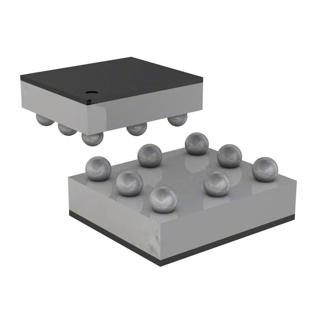
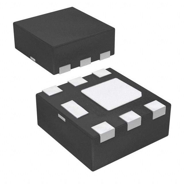
NCP360, NCV360 PACKAGE DIMENSIONS UDFN6 2x2, 0.65P CASE 517AB ISSUE B NOTES: D A 1. DIMENSIONING AND TOLERANCING PER B ASME Y14.5M, 1994. 2. CONTROLLING DIMENSION: MILLIMETERS. 3. COPLANARITY APPLIES TO THE EXPOSED PAD AS WELL AS THE TERMINALS. MILLIMETERS ÍÍÍ DIM MIN MAX A 0.45 0.55 E A1 0.00 0.05 PIN ONE ÍÍÍ A3 0.127 REF REFERENCE b 0.25 0.35 ÍÍÍ D 2.00 BSC D2 1.50 1.70 2X 0.10 C E 2.00 BSC E2 0.80 1.00 e 0.65 BSC 2X 0.10 C K 0.20 --- L 0.25 0.35 A3 0.10 C SOLDERING FOOTPRINT* 6X A 0.95 0.47 6X 0.08 C 6X A1 0.40 C SEATING 1 PLANE D2 6XL e 4X 1.70 1 3 E2 0.65 PITCH 2.30 6XK 6 4 6Xb DIMENSIONS: MILLIMETERS 0.10 C A B *For additional information on our Pb−Free strategy and soldering BOTTOM VIEW 0.05 C details, please download the ON Semiconductor Soldering and Mounting Techniques Reference Manual, SOLDERRM/D. http://onsemi.com 12
NCP360, NCV360 PACKAGE DIMENSIONS TSOP−5 CASE 483−02 ISSUE H NOTES: 1. DIMENSIONING AND TOLERANCING PER NOTE 5 D5X ASME Y14.5M, 1994. 2. CONTROLLING DIMENSION: MILLIMETERS. 2X 0.10 T 0.20 C A B 3. MLEAAXDIM FUINMIS LHE ATDH ITCHKINCEKSNSE.S MSI NINIMCULUMD LEESAD THICKNESS IS THE MINIMUM THICKNESS M OF BASE MATERIAL. 2X 0.20 T 5 4 B S 4. DMIOMLEDN FSLIOANSHS ,A P ARNODT RBU DSOIO NNOST, OINRC GLUATDEE 1 2 3 BURRS. K 5. OPTIONAL CONSTRUCTION: AN L DETAIL Z ADDITIONAL TRIMMED LEAD IS ALLOWED G IN THIS LOCATION. TRIMMED LEAD NOT TO EXTEND MORE THAN 0.2 FROM BODY. A MILLIMETERS DIM MIN MAX DETAIL Z A 3.00 BSC J B 1.50 BSC C C 0.90 1.10 0.05 H SPELAATNIENG DG 0.02.595 BS0C.50 H 0.01 0.10 T J 0.10 0.26 K 0.20 0.60 L 1.25 1.55 M 0 (cid:3) 10 (cid:3) S 2.50 3.00 SOLDERING FOOTPRINT* 1.9 0.074 0.95 0.037 2.4 0.094 1.0 0.039 0.7 (cid:3) (cid:4) 0.028 SCALE 10:1 mm inches *For additional information on our Pb−Free strategy and soldering details, please download the ON Semiconductor Soldering and Mounting Techniques Reference Manual, SOLDERRM/D. ON Semiconductor and are registered trademarks of Semiconductor Components Industries, LLC (SCILLC). SCILLC reserves the right to make changes without further notice to any products herein. SCILLC makes no warranty, representation or guarantee regarding the suitability of its products for any particular purpose, nor does SCILLC assume any liability arising out of the application or use of any product or circuit, and specifically disclaims any and all liability, including without limitation special, consequential or incidental damages. “Typical” parameters which may be provided in SCILLC data sheets and/or specifications can and do vary in different applications and actual performance may vary over time. All operating parameters, including “Typicals” must be validated for each customer application by customer’s technical experts. SCILLC does not convey any license under its patent rights nor the rights of others. SCILLC products are not designed, intended, or authorized for use as components in systems intended for surgical implant into the body, or other applications intended to support or sustain life, or for any other application in which the failure of the SCILLC product could create a situation where personal injury or death may occur. Should Buyer purchase or use SCILLC products for any such unintended or unauthorized application, Buyer shall indemnify and hold SCILLC and its officers, employees, subsidiaries, affiliates, and distributors harmless against all claims, costs, damages, and expenses, and reasonable attorney fees arising out of, directly or indirectly, any claim of personal injury or death associated with such unintended or unauthorized use, even if such claim alleges that SCILLC was negligent regarding the design or manufacture of the part. SCILLC is an Equal Opportunity/Affirmative Action Employer. This literature is subject to all applicable copyright laws and is not for resale in any manner. PUBLICATION ORDERING INFORMATION LITERATURE FULFILLMENT: N. American Technical Support: 800−282−9855 Toll Free ON Semiconductor Website: www.onsemi.com Literature Distribution Center for ON Semiconductor USA/Canada P.O. Box 5163, Denver, Colorado 80217 USA Europe, Middle East and Africa Technical Support: Order Literature: http://www.onsemi.com/orderlit Phone: 303−675−2175 or 800−344−3860 Toll Free USA/Canada Phone: 421 33 790 2910 Fax: 303−675−2176 or 800−344−3867 Toll Free USA/Canada Japan Customer Focus Center For additional information, please contact your loca Email: orderlit@onsemi.com Phone: 81−3−5817−1050 Sales Representative http://onsemi.com NCP360/D 13
Mouser Electronics Authorized Distributor Click to View Pricing, Inventory, Delivery & Lifecycle Information: O N Semiconductor: NCP360SNT1G NCP360SNAET1G NCP360SNAFT1G NCP360MUTBG NCP360SNAIT1G NCV360SNAET1G