ICGOO在线商城 > NCP1606BOOSTGEVB
 Datasheet下载
- 型号: NCP1606BOOSTGEVB
- 制造商: ON Semiconductor
- 库位|库存: xxxx|xxxx
- 要求:
| 数量阶梯 | 香港交货 | 国内含税 |
| +xxxx | $xxxx | ¥xxxx |
查看当月历史价格
查看今年历史价格
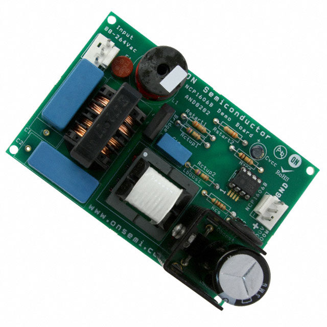
NCP1606BOOSTGEVB产品简介:
ICGOO电子元器件商城为您提供NCP1606BOOSTGEVB由ON Semiconductor设计生产,在icgoo商城现货销售,并且可以通过原厂、代理商等渠道进行代购。 提供NCP1606BOOSTGEVB价格参考以及ON SemiconductorNCP1606BOOSTGEVB封装/规格参数等产品信息。 你可以下载NCP1606BOOSTGEVB参考资料、Datasheet数据手册功能说明书, 资料中有NCP1606BOOSTGEVB详细功能的应用电路图电压和使用方法及教程。
| 参数 | 数值 |
| 产品目录 | 编程器,开发系统 |
| 描述 | EVAL BOARD FOR NCP1606BOOSTG |
| 产品分类 | |
| 品牌 | ON Semiconductor |
| 数据手册 | |
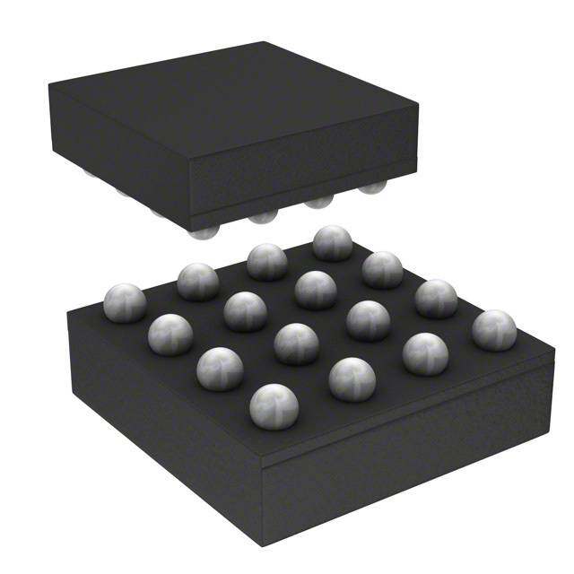
| 产品图片 |
|
| 产品型号 | NCP1606BOOSTGEVB |
| rohs | 无铅 / 符合限制有害物质指令(RoHS)规范要求 |
| 产品系列 | - |
| 主要用途 | AC/DC,主面和辅面,带 PFC |
| 使用的IC/零件 | NCP1606 |
| 其它名称 | NCP1606BOOSTGEVBOS |
| 功率-输出 | 100W |
| 所含物品 | 板 |
| 板类型 | 完全填充 |
| 标准包装 | 1 |
| 电压-输入 | 88 ~ 264 VAC |
| 电压-输出 | 400V |
| 电流-输出 | 250mA |
| 相关产品 | /product-detail/zh/NCP1606BPG/NCP1606BPG-ND/1638131/product-detail/zh/NCP1606APG/NCP1606APG-ND/1638130/product-detail/zh/NCP1606BDR2G/NCP1606BDR2GOSDKR-ND/1630424/product-detail/zh/NCP1606ADR2G/NCP1606ADR2GOSDKR-ND/1630423/product-detail/zh/NCP1606BDR2G/NCP1606BDR2GOSCT-ND/1630374/product-detail/zh/NCP1606ADR2G/NCP1606ADR2GOSCT-ND/1630373/product-detail/zh/NCP1606BDR2G/NCP1606BDR2GOSTR-ND/1630324/product-detail/zh/NCP1606ADR2G/NCP1606ADR2GOSTR-ND/1630323 |
| 稳压器拓扑 | 升压 |
| 设计资源 | 点击此处下载产品Datasheethttp://www.onsemi.com/pub/Collateral/NCP1606BOOSTGEVB_GERBER.ZIP点击此处下载产品Datasheet |
| 输出和类型 | 1,隔离 |
| 频率-开关 | 250kHz |


- 商务部:美国ITC正式对集成电路等产品启动337调查
- 曝三星4nm工艺存在良率问题 高通将骁龙8 Gen1或转产台积电
- 太阳诱电将投资9.5亿元在常州建新厂生产MLCC 预计2023年完工
- 英特尔发布欧洲新工厂建设计划 深化IDM 2.0 战略
- 台积电先进制程称霸业界 有大客户加持明年业绩稳了
- 达到5530亿美元!SIA预计今年全球半导体销售额将创下新高
- 英特尔拟将自动驾驶子公司Mobileye上市 估值或超500亿美元
- 三星加码芯片和SET,合并消费电子和移动部门,撤换高东真等 CEO
- 三星电子宣布重大人事变动 还合并消费电子和移动部门
- 海关总署:前11个月进口集成电路产品价值2.52万亿元 增长14.8%


PDF Datasheet 数据手册内容提取
NCP1606 Cost Effective Power Factor Controller The NCP1606 is an active power factor controller specifically designed for use as a pre−converter in electronic ballasts, ac−dc adapters and other medium power off line converters (typically up to 300W). It embeds a Critical Conduction Mode (CRM) scheme that http://onsemi.com substantially exhibits unity power factor across a wide range of input MARKING voltages and power levels. Housed in a DIP8 or SOIC−8 package, the 8 DIAGRAMS NCP1606 minimizes the number of external components. Its integration of comprehensive safety protection features makes it an 1 8 excellent driver for rugged PFC stages. SO−8 1606x D SUFFIX ALYW General Features CASE 751 (cid:2) 1 • “Unity” Power Factor • No Need for Input Voltage Sensing • Latching PWM for Cycle by Cycle On Time Control (Voltage Mode) 8 NCP1606x • High Precision Voltage Reference (±1.6% over temperature ranges) 1 Y Y WAWWLG • Very Low Startup Current Consumption (≤ 40 (cid:2)A) DIP−8 • P SUFFIX Low Typical Operating Current (2.1 mA) CASE 626 • −500 mA / +800 mA Totem Pole Gate Driver x = A or B • Undervoltage Lockout with Hysteresis A = Assembly Location • L, WL = Wafer Lot Pin to Pin Compatible with Industry Standards Y, YY = Year W, WW = Work Week Safety Features (cid:2) or G = Pb−Free Package • Programmable Overvoltage Protection • Protection against Open Loop (Undervoltage Protection) PIN CONNECTION • Accurate and Programmable On Time Limitation • Feedback VCC Overcurrent Limitation Control Drive Ct Ground Typical Applications CS ZCD/STDWN • (Top View) Electronic Light Ballast • AC Adapters, TVs, Monitors ORDERING INFORMATION • All Off Line Appliances Requiring Power Factor Correction See detailed ordering and shipping information in the package dimensions section on page 20 of this data sheet. LBOOST VOUT DBOOST LOAD RZCD (Ballast, + ROUT1 NCP1606 VCC SMPS, etc.) EMI Cin 1 FB VCC 8 +CBULK AC Line 2 7 Filter Ccomp Ctrl DRV 3 6 ROUT2 Ct GND 4 5 CS ZCD Ct RSENSE Figure 1. Typical Application © Semiconductor Components Industries, LLC, 2010 1 Publication Order Number: June, 2010 − Rev. 8 NCP1606/D
NCP1606 VCC Shutdown VOUT nPOK VCC − UVP CBULK ROUT1 + 30+0 ESD + +−UVLO VVDDDDGD mV FB E/A (Enable EA) Dynamic OVP VDD Reg − ESD + Isink>Iovp DBOOST ROUT2 + IEAMsienaksure Fault uVDD 2.5 V VDD Static OVP CCOMP VCONTROELnable CVlaEmALp Swthaetinc cOlaVmPp i sis t raigcgtievraetedd. Control ESD VEAH Clamp AC IN LBOOST nPOK VDD PWM Ct 270 (cid:2)A Add VEAL − Offset + ESD Ct S Q DRV LEB + OCP R Q CS ESD + − VCC RSENSE VCS(limit) Demag UVLO VDD +− S Q S Q DRV + 2.1 V VACcLt(iNvEeG ) +− RQ RQ VddGD Clamp + Off Timer ZCD −1.6 V Reset S Q uVDD RZCD + + Shutdown RQ GND 200 mV VCClLa(PmOpS) uVDD S Q POK RQ nPOK *All SR Latches are Reset Dominant *All values shown are typical only. Refer to the “Electrical Characteristics” for complete specifications. Figure 2. Block Diagram http://onsemi.com 2
NCP1606 PIN FUNCTION DESCRIPTION Pin Number Name Function 1 Feedback (FB) The FB pin makes available the inverting input of the internal error amplifier. A simple resistor divider scales and delivers the output voltage to the FB pin to maintain regulation. The feedback information is also used for the programmable overvoltage and undervoltage protections. 2 Control The regulation block output is available on this pin. A compensation network is placed between FB and Control to set the loop bandwidth low enough to yield a high power factor ratio and a low THD. 3 Ct The Ct pin sources a 270 (cid:2)A current to charge an external timing capacitor. The circuit controls the power switch on time by comparing the Ct voltage to an internal voltage derived from the regulation block. 4 Current Sense This pin limits the pulse by pulse current through the switch MOSFET when connected as show in (CS) Figure 1. When the voltage exceeds 1.7 V (A version) or 0.5 V (B version), the drive turns off. The maximum switch current can be adjusted by changing the sense resistor. 5 Zero Current The voltage of an auxiliary winding should be applied to this pin to detect the moment when the coil is Detection (ZCD) demagnetized for critical conduction mode operation. Ground ZCD to shutdown the part. 6 Ground (GND) Connect this pin to the pre−converter ground. 7 Drive (DRV) The powerful integrated driver is suitable to effectively switch a high gate charge power MOSFET. 8 VCC This pin is the positive supply of the IC. The circuit starts to operate when VCC exceeds 12 V (typ) and turns off when VCC goes below 9.5 V (typ). After startup, the operating range is 10.3 V to 20 V. MAXIMUM RATINGS Rating Symbol Value Unit Supply Voltage VCC −0.3 to 20 V Supply Current ICC ±20 mA DRV Voltage VDRV −0.3 to 20 V DRV Current IDRV −800 to 500 mA FB Voltage VFB −0.3 to 10 V FB Current IFB ±10 mA Control Voltage VControl −0.3 to 10 V Control Current IControl −2 to 10 mA Ct Voltage VCt −0.3 to 6 V Ct Current ICt ±10 mA CS Voltage VCS −0.3 to 6 V CS Current ICS ±10 mA ZCD Voltage VZCD −0.3 to 10 V ZCD Current IZCD ±10 mA Power Dissipation and Thermal Characteristics P suffix, Plastic Package, Case 626 Maximum Power Dissipation @ TA = 70°C PD(DIP) 800 mW Thermal Resistance Junction−to−Air R(cid:3)JA(DIP) 100 °C/W D suffix, Plastic Package, Case 751 Maximum Power Dissipation @ TA = 70°C PD(SO) 450 mW Thermal Resistance Junction−to−Air R(cid:3)JA(SO) 178 °C/W Operating Junction Temperature Range TJ −40 to +125 °C Maximum Junction Temperature TJ(MAX) 150 °C Storage Temperature Range TSTG −65 to 150 °C Lead Temperature (Soldering, 10 s) TL 300 °C Stresses exceeding Maximum Ratings may damage the device. Maximum Ratings are stress ratings only. Functional operation above the Recommended Operating Conditions is not implied. Extended exposure to stresses above the Recommended Operating Conditions may affect device reliability. 1. This device series contains ESD protection and exceeds the following tests: Pins 1−6, 8: Human Body Model 2000 V per JEDEC Standard JESD22−A114E, Machine Model Method 200 V per JEDEC Standard JESD22−A115−A Pin 7: Human Body Model 2000 V per JEDEC Standard JESD22−A114E, Machine Model Method 180 V per JEDEC Standard JESD22−A115−A 2. This device contains latch−up protection and exceeds ±100 mA per JEDEC Standard JESD78. http://onsemi.com 3
NCP1606 ELECTRICAL CHARACTERISTICS (Unless otherwise specified: For typical values, TJ = 25°C. For min/max values, TJ = −40°C to +125°C, VCC = 12 V, FB = 2.4 V, CDRV = 1nF, Ct = 1 nF, CS = 0 V, Control = open, ZCD = open) Symbol Rating Min Typ Max Unit VCC UNDERVOLTAGE LOCKOUT SECTION VCC(on) VCC Startup Threshold (Undervoltage Lockout Threshold, Vcc rising) V −25°C < TJ < +125°C 11.0 12.0 13.0 −40°C < TJ < +125°C 10.9 12.0 13.1 VCC(off) VCC Disable Voltage after Turn On (Undervoltage Lockout Threshold, VCC falling) V −25°C < TJ < +125°C 8.7 9.5 10.3 −40°C < TJ < +125°C 8.5 9.5 10.5 HUVLO Undervoltage Lockout Hysteresis 2.2 2.5 2.8 V DEVICE CONSUMPTION ICC(startup) Icc consumption during startup: 0 V < VCC < VCC(on) − 200 mV − 20 40 (cid:2)A ICC1 Icc consumption after turn on at VCC = 12 V, No Load, 70 kHz switching − 1.4 2.0 mA ICC2 Icc consumption after turn on at VCC = 12 V, 1 nF Load, 70 kHz switching − 2.1 3 mA ICC(fault) Icc consumption after turn on at VCC = 12 V, 1 nF Load, no switching − 1.2 1.6 mA (such as during OVP fault, UVP fault, or grounding ZCD) REGULATION BLOCK (ERROR AMPLIFIER) VREF Voltage Reference @ TJ = 25 °C 2.475 2.50 2.525 V −25°C < TJ < +125°C 2.465 2.50 2.535 −40°C < TJ < +125°C 2.460 2.50 2.540 VREF(line) Vref Line Regulation from VCC(on) + 200 mV < VCC < 20 V, @ TJ = 25°C −2 − 2 mV IEA Error Amplifier Current Capability:: (Note 3) mA Sink (Control = 4 V, VFB = 2.6 V): 8.0 17 30 Source (Control = 4 V, VFB = 2.4 V): −20 −6.0 −2 GOL Open Loop, Error Amplifier Gain (Note 4) − 80 − dB BW Unity Gain Bandwidth (Note 4) − 1 − MHz IFB FB Bias Current @ VFB = 3 V −500 − 500 nA IControl Control Pin Bias Current @ FB = 0 V and Control = 4.0 V. −1 − 1 (cid:2)A VEAH VCONTROL @ IEASOURCE = 0.5 mA, VFB = 2.4 V 4.9 5.3 5.7 V VEAL VCONTROL @ IEASINK = 0.5 mA, VFB = 2.6 V 1.85 2.1 2.4 V VEA(diff) VEA(diff) = VEAH − VEAL. Difference between max and min Control voltages 3.0 3.2 3.4 V CURRENT SENSE BLOCK VCS(limit) Overcurrent Protection Threshold: V NCP1606A 1.6 1.7 1.8 NCP1606B 0.45 0.5 0.55 tLEB Leading Edge Blanking duration 150 250 350 ns tCS Overcurrent protection propagation delay. 40 100 170 ns ICS CS bias current @ VCS = 2 V −1 − 1 (cid:2)A ZERO CURRENT DETECTION VZCDH Zero Current Detection Threshold (VZCD rising) 1.9 2.1 2.3 V VZCDL Zero Current Detection Threshold (VZCD falling) 1.45 1.6 1.75 V VZCD(HYS) VZCDH − VZCDL 300 500 800 mV IZCD Maximum ZCD bias Current @ VZCD = 5 V −2 − +2 (cid:2)A VCL(POS) Upper Clamp Voltage @ IZCD = 2.5 mA 5 5.7 6.5 V ICL(POS) Current Capability of the Positive Clamp at VZCD = VCL(POS) + 200 mV: 5.0 8.5 − mA 3. Parameter values are valid for transient conditions only. 4. Parameter characterized and guaranteed by design, but not tested in production. http://onsemi.com 4
NCP1606 ELECTRICAL CHARACTERISTICS (Unless otherwise specified: For typical values, TJ = 25°C. For min/max values, TJ = −40°C to +125°C, VCC = 12 V, FB = 2.4 V, CDRV = 1nF, Ct = 1 nF, CS = 0 V, Control = open, ZCD = open) Symbol Rating Min Typ Max Unit VCL(NEG) Negative Active Clamp Voltage @ IZCD = −2.5 mA 0.45 0.6 0.75 V ICL(NEG) Current Capability of the Negative Active Clamp: in normal mode (VZCD = 300 mV) 2.5 3.7 5.0 mA in shutdown mode (VZCD = 100 mV) 35 70 100 (cid:2)A VSDL Shutdown Threshold (VZCD falling) 150 200 250 mV VSDH Enable Threshold (VZCD rising) − 290 350 mV VSDHYS Shutdown Comparator Hysteresis − 90 − mV tZCD Zero current detection propagation delay − 100 170 ns tSYNC Minimum detectable ZCD pulse width − 70 − ns tSTART Drive off restart timer 75 180 300 (cid:2)s RAMP CONTROL ICHARGE Charge Current (VCT = 0 V) −25°C < TJ < +125°C 243 270 297 (cid:2)A −40°C < TJ < +125°C 235 270 297 tCT(discharge) Time to discharge a 1 nF Ct capacitor from VCT = 3.4 V to 100 mV. − − 100 ns VCTMAX Maximum Ct level before DRV switches off −25°C < TJ < +125°C 2.9 3.2 3.3 V −40°C < TJ < +125°C 2.9 3.2 3.4 tPWM Propagation delay of the PWM comparator − 150 220 ns OVER AND UNDERVOLTAGE PROTECTION IOVP Dynamic overvoltage protection (OVP) triggering current: (cid:2)A NCP1606A 34 40 45 NCP1606B @ TJ = 25°C 9.0 10.4 11.8 NCP1606B @ TJ = −40°C to +125°C 8.7 − 12.1 IOVP(HYS) Hysteresis of the dynamic OVP current before the OVP latch is released: (cid:2)A NCP1606A − 30 − NCP1606B − 8.5 − VOVP Static OVP Threshold Voltage VEAL + V 100mV VUVP Undervoltage protection (UVP) threshold voltage 0.25 0.3 0.4 V GATE DRIVE SECTION Gate Drive Resistance: (cid:4) ROH ROH @ ISOURCE = 100 mA − 12 18 ROH @ ISOURCE = 20 mA − 12 18 ROL ROL @ ISINK = 100 mA − 6 10 ROL @ ISINK = 20 mA − 6 10 trise Drive voltage rise time from 10% VCC to 90% VCC with CDRV = 1 nF and VCC = 12V. − 30 80 ns tfall Drive voltage fall time from 90% VCC to 10% VCC with CDRV = 1 nF and VCC = 12V. − 25 70 ns VOUT(start) Driver output voltage at VCC = VCC(on) − 200 mV and Isink = 10 mA − − 0.2 V 3. Parameter values are valid for transient conditions only. 4. Parameter characterized and guaranteed by design, but not tested in production. http://onsemi.com 5
NCP1606 TYPICAL CHARACTERISTICS A) 274 14 (cid:2) T ( 272 12 N E Ct = 1 nF R R 270 10 CU s) GE 268 (cid:2)E ( 8 R M CHA 266 N TI 6 R O O 264 4 T A L L 262 2 CI S O 260 0 −50 −25 0 25 50 75 100 125 150 0 1 2 3 4 5 6 TEMPERATURE (°C) VCONTROL (V) Figure 3. Oscillator Charge Current (I ) Figure 4. Typical On Time (T ) vs. V CHARGE ON CONTROL vs. Temperature Level 3.30 170 s) n L (V) 3.25 ELAY ( 160 E 3.20 D EV N L O Ct 3.15 TI 150 M GA U A M P XI 3.10 RO MA M P 140 3.05 W P 3.00 130 −50 −25 0 25 50 75 100 125 150 −50 −25 0 25 50 75 100 125 150 TEMPERATURE (°C) TEMPERATURE (°C) Figure 5. Maximum Ct Level (V ) vs. Figure 6. PWM Comparator Propagation Delay CTMAX Temperature (t ) vs. Temperature PWM 2.505 100 200 2.500 V) 80 160 E ( GAIN G2.495 A 60 120 E VOLT2.490 N (dB)40 PHASE 80°SE () NC2.485 GAI HA RE 20 40P E2.480 F E R 0 0 2.475 2.470 −20 −40 −50 −25 0 25 50 75 100 125 150 10E+0100E+0 1E+3 10E+3 100E+3 1E+6 10E+6 TEMPERATURE (°C) FREQUENCY (Hz) Figure 7. Reference Voltage (V ) vs. Figure 8. Error Amplifier Open Loop Gain (G ) REF OL Temperature and Phase http://onsemi.com 6
NCP1606 TYPICAL CHARACTERISTICS 45 12 A) A) (cid:2)T ( 40 IOVP (cid:2)T ( 11 N N IOVP E E R R R 35 R 10 U U C C P P V V O 30 O 9 MIC IOVP(HYS) MIC IOVP(HYS) A A N 25 N 8 Y Y D D 20 7 −50 −25 0 25 50 75 100 125 150 −50 −25 0 25 50 75 100 125 150 TEMPERATURE (°C) TEMPERATURE (°C) Figure 9. Overvoltage Activation Current vs. Figure 10. Overvoltage Activation Current vs. Temperature for the A Version Temperature for the B Version A) 2.20 24 m ) (22.15 22 CC A) T (I (cid:2)T ( 20 N 2.10 N E E R R 18 R R U 2.05 U C C Y P 16 UPPL 2.00 RTU 14 S TA G 1.95 S N 12 HI C T 1.90 10 WI −50 −25 0 25 50 75 100 125 150 −50 −25 0 25 50 75 100 125 150 S TEMPERATURE (°C) TEMPERATURE (°C) Figure 11. Supply Current (I ) vs. Figure 12. Startup Current I vs. CC2 CC(startup) Temperature Temperature 13 200 VCC(on) 12 V) s) 190 GE ( (cid:2)R ( A 11 E T M OL TI 180 V T PLY 10 VCC(off) TAR P S U E S R 170 9 8 160 −50 −25 0 25 50 75 100 125 150 −50 −25 0 25 50 75 100 125 150 TEMPERATURE (°C) TEMPERATURE (°C) Figure 13. Supply Voltage Thresholds vs. Figure 14. Restart Timer (t ) vs. START Temperature Temperature http://onsemi.com 7
NCP1606 TYPICAL CHARACTERISTICS 18 280 (cid:4)) 16 E ( s) NC 14 ROH N (n 270 STA 12 TIO SI A E 10 R VE R 8 R DU 260 DRI 6 ROL LTE T FI U 4 B 250 P E T L U 2 O 0 240 −50 −25 0 25 50 75 100 125 150 −50 −25 0 25 50 75 100 125 150 TEMPERATURE (°C) TEMPERATURE (°C) Figure 15. Output Gate Drive Resistance (R Figure 16. LEB Duration (t ) vs. Temperature OH LEB and R ) at 100 mA vs. Temperature OL V) 1.710 0.520 V) D ( D ( L L O 1.705 0.515 O H H S A S E 1.700 0.510 E R R H H T 1.695 0.505 T T T N B N E 1.690 0.500 E R R R R CU 1.685 0.495 CU R R E E V 1.680 0.490 V O O N 1.675 0.485 N O O SI SI R 1.670 0.480 R E −50 −25 0 25 50 75 100 125 150 E V V A TEMPERATURE (°C) B Figure 17. Overcurrent Threshold V vs. CS(limit) Temperature 0.320 0.35 0.315 V) V)0.310 LD ( 0.30 VSDH D ( HO L0.305 S O E H R ES0.300 TH 0.25 HR N T0.295 W VP DO VSDL U0.290 T 0.20 U H 0.285 S 0.280 0.15 −50 −25 0 25 50 75 100 125 150 −50 −25 0 25 50 75 100 125 150 TEMPERATURE (°C) TEMPERATURE (°C) Figure 18. Undervoltage Protection Threshold Figure 19. Shutdown Thresholds vs. (V ) vs. Temperature Temperature UVP http://onsemi.com 8
NCP1606 Introduction NCP1606B uses a lower overcurrent threshold, which The NCP1606 is a voltage mode power factor correction can further reduce the application’s power dissipation. (PFC) controller designed to drive cost effective An integrated LEB filter reduces the chance of noise pre−converters to meet input line harmonic regulations. prematurely triggering the overcurrent limit. This controller operates in critical conduction mode • Shutdown Features. The PFC pre−converter can be (CRM) for optimal performance in applications up to about easily placed in a shutdown mode by grounding either 300W. Its voltage mode scheme enables it to obtain unity the FB pin or the ZCD pin. During this mode, the I CC power factor without the need for a line sensing network. current consumption is reduced and the error amplifier The output voltage is accurately controlled by a high is disabled. precision error amplifier. The controller also implements a comprehensive array of safety features for robust designs. Application information The key features of the NCP1606 are as follows: Most electronic ballasts and switching power supplies • Constant on time (Voltage Mode) CRM operation. use a diode bridge rectifier and a bulk storage capacitor to High power factor ratios are easily obtained without produce a dc voltage from the utility ac line (Figure 20). the need for input voltage sensing. This allows for This DC voltage is then processed by additional circuitry optimal standby power consumption. to drive the desired output. • Accurate and Programmable On Time Limitation. The Rectifiers Converter NCP1606 using an accurate current source and an external capacitor to generate the on time. AC • High Precision Voltage Reference. The error amplifier Line + Bulk reference voltage is guaranteed at 2.5 V ±1.6% over Storage Load Capacitor process and temperature. This results in very accurate output voltages. • Very Low Startup Consumption. The circuit Figure 20. Typical Circuit without PFC consumption is reduced to a minimum (< 40 (cid:2)A) This simple rectifying circuit draws power from the line during the startup phase which allows fast, low loss, when the instantaneous ac voltage exceeds the capacitor charging of V . The architecture of the NCP1606 CC voltage. Since this occurs near the line voltage peak, the gives a controlled undervoltage lockout level and resulting current draw is non sinusoidal and contains a very provides ample V hysteresis during startup. CC • high harmonic content. This results in a poor power factor Powerful Output Driver. A −500 mA / +800 mA totem (typically < 0.6) and consequently, the apparent input pole gate driver is used to provide rapid turn on and power is much higher than the real power delivered to the turn off times. This translates into improved load. Additionally, if multiple devices are tied to the same efficiencies and the ability to drive higher power input line, the effect is magnified and a “line sag” effect can MOSFETs. Additionally, a combination of active and be produced (see Figure 21). passive circuitry is used to ensure that the driver output voltage does not float high while V is below CC Vpk its turn on level. • Rectified DC Programmable Overvoltage Protection (OVP). The 0 adjustable OVP feature protects the PFC stage against Line excessive output overshoots that could damage the Sag application. These events can typically occur during AC Line Voltage the startup phase or when the load is abruptly removed. The NCP1606B gives a lower OVP 0 threshold, which can further reduce the application’s AC Line Current standby power loss. • Protection against Open Loop (Undervoltage Protection). Undervoltage protection (UVP) disables Figure 21. Typical Line Waveforms without PFC the PFC stage when the output voltage is excessively low. This also protects the circuit in case of a failure in Increasingly, government regulations and utility the feedback network: if no voltage is applied to FB requirements necessitate control over the line current because of a bad connection, UVP is activated and harmonic content. To meet this need, power factor shuts down the pre−converter. correction is implemented with either a passive or active • Overcurrent Limitation. The peak current is accurately circuit. Passive circuits usually contain a combination of limited on a pulse by pulse basis. The level is large capacitors, inductors, and rectifiers that operate at the adjustable by modifying the switch sense resistor. The ac line frequency. Active circuits incorporate some form of http://onsemi.com 9
NCP1606 a high frequency switching converter which regulates the ac line, thus significantly reducing the harmonic current input current to stay in phase with the input voltage. These content. Because of these advantages, active PFC circuits circuits operate at a higher frequency and so they are have become the most popular way to meet harmonic smaller, lighter in weight, and more efficient than a passive content requirements. Generally, they consist of inserting circuit. With proper control of an active PFC stage, almost a PFC pre−regulator between the rectifier bridge and the any complex load can be made to appear in phase with the bulk capacitor (Figure 22). Rectifiers PFC Preconverter Converter AC Line High Bulk + Frequency + Storage Load Bypass NCP1606 Capacitor Capacitor Figure 22. Active PFC Pre−Converter with the NCP1606 The boost (or step up) converter is the most popular (DCM) and continuous conduction mode (CCM). In CRM, topology for active power factor correction. With the the next driver on time is initiated when the boost inductor proper control, it produces a constant voltage while current reaches zero. CRM operation is an ideal choice for drawing a sinusoidal current from the line. For medium medium power PFC boost stages because it combines the power (<300 W) applications, critical conduction mode lower peak currents of CCM operation with the zero current (also called borderline conduction mode) is the preferred switching of DCM operation. The operation and control method. Critical conduction mode (CRM) occurs at waveforms in a PFC boost converter are illustrated in the boundary between discontinuous conduction mode Figure 23. Diode Bridge Icoil Diode Bridge Icoil + Vin Vd + Vin Vd L L + + + IN IN VOUT − − The power switch is ON The power switch is OFF The power switch being about zero, the input voltage The coil current flows through the diode. The coil voltage is (VOUT − is applied across the coil. The coil current linearly Vin) and the coil current linearly decays with a (VOUT − Vin)/L slope. increases with a (Vin/L) slope. Coil Current Vin/L (VOUT − Vin)/L Critical Conduction Mode: Icoil_pk Next current cycle starts as soon as the core is reset. Vd VOUT Vin If next cycle does not start then Vd rings towards Vin Figure 23. Schematic and Waveforms of an Ideal CRM Boost Converter http://onsemi.com 10
NCP1606 When the switch is closed, the inductor current increases Vin(t) linearly to its peak value. When the switch opens, the Vinpk inductor current linearly decreases to zero. At this point, ILpk IL(t) the drain voltage of the switch (V ) is essentially floating d and begins to drop. If the next switching cycle does not start, then the voltage will ring with a dampened frequency Iinpk Iin(t) around V . A simple derivation of equations (such as found in in AND8123), leads to the result that good power factor correction in CRM operation is achieved when the on time is constant across an ac cycle and is equal to: ON 2(cid:3)P (cid:3)L MOSFET ton(cid:2)(cid:5)(cid:3)VaOcUT 2 (eq. 1) OFF RMS A simple plot of this switching over an ac line cycle is Figure 24. Inductor Waveform During CRM Operation illustrated in Figure 24. The off time varies based on the instantaneous line voltage, but the on time is kept constant. ERROR AMPLIFIER REGULATION This naturally causes the peak inductor current (ILpk) to The NCP1606 is configured to regulate the boost output follow the ac line voltage. voltage based on its built in error amplifier (EA). The error The NCP1606 represents an ideal method to implement amplifier’s negative terminal is pinned out to FB, the this constant on time CRM control in a cost effective and positive terminal is tied to a 2.5 V ± 1.6% reference, and the robust solution. The device incorporates an accurate output is pinned out to Control (Figure25). regulation circuit, a low power startup circuit, and advanced protection features. VOUT ROUT1 EA PWM BLOCK FB − + + 2.5 V tON(max) ROUT2 CCOMP Slope(cid:2)I Ct CHARGE VCONTROL tON Control tPWM VEAL VEAH VCONTROL Figure 25. Error Amplifier and On Time Regulation Circuits A resistor divider from the boost output to the input of the (2.5V). The output voltage can then be easily set according EA sets the FB level. If the output voltage is too low, then to the following equation: the FB level will drop and the EA will cause the control R (cid:4)R voltage to increase. This increases the on time of the driver, V (cid:2)2.5V(cid:3) OUT1 OUT2 (eq. 2) OUT R which increases the power delivered and brings the output OUT2 A compensation network is placed between the FB and back into regulation. Alternatively, if the output voltage Control pins to reduce the speed at which the EA responds (and hence FB voltage) is too high, then the control level to changes in the boost output. This is necessary due to the decreases and the driver on times are shortened. In this way, nature of an active PFC circuit. The PFC stage absorbs a the circuit regulates the output voltage (V ) so that the OUT sinusoidal current from a sinusoidal line voltage. Hence, V portion that is applied to FB through the resistor OUT the converter provides the load with a power that matches divider R and R is equal to the internal reference OUT1 OUT2 http://onsemi.com 11
NCP1606 the average demand only. Therefore, the output capacitor power. Alternatively, when the supplied power is higher must “absorb” the difference between the delivered power than that absorbed by the load, the output capacitor charges and the power consumed by the load. This means that when to store the excess energy. The situation is depicted in the power fed to the load is lower than the demand, the Figure 26. output capacitor discharges to compensate for the lack of Iac Vac PIN POUT VOUT Figure 26. Output Voltage Ripple for a Constant Output Power As a consequence, the output voltage exhibits a ripple at a frequency of either 100 Hz (for 50 Hz mains such as in Control VCONTROL Europe) or 120 Hz (for 60 Hz mains in the USA). This ripple must not be taken into account by the regulation loop because the error amplifier’s output voltage must be kept VDD constant over a given ac line cycle for a proper shaping of PWM the line current. Due to this constraint, the regulation ICHARGE − Ct bandwidth is typically set below 20 Hz. For a simple type1 + + tON compensation network, only a capacitor is placed between FB and Control (see Figure 1). In this configuration, the DRV capacitor necessary to attenuate the bulk voltage ripple is VEAL given by: VCt VCONTROL − VEAL G VCt(off) 1020 CCOMP(cid:2)4(cid:3)(cid:6)f (cid:3)R (eq. 3) line OUT1 where G is the attenuation level in dB (commonly 60 dB) ON TIME SEQUENCE tON Since the NCP1606 is designed to control a CRM boost DRV converter, its switching pattern must accommodate constant on times and variable off times. The Controller generates the on time via an external capacitor connected Figure 27. On Time Generation to pin 3 (Ct). A current source charges this capacitor to a level determined by the Control pin voltage. Specifically, Since V varies with the RMS line level and CONTROL Ct is charged to VCONTROL minus the VEAL offset output load, this naturally satisfies equation 1. And if the (typically 2.1V). Once this level is exceeded, the drive is values of compensation components are sufficient to filter turned off (Figure 27). http://onsemi.com 12
NCP1606 out the bulk voltage ripple, then this on time is truly constant over the ac line cycle. Note that the maximum on time of the controller occurs DRIVE when VCONTROL is at its maximum. Therefore, the Ct VOUT capacitor must be sized to ensure that the required on time can be delivered at full power and the lowest input voltage Drain condition. The maximum on time is given by: Ct(cid:3)V t (cid:2) CTMAX (eq. 4) ON(max) I CHARGE ZCD Combining this equation with equation 1, gives: Winding 2(cid:3)P (cid:3)L(cid:3)I Ct(cid:5) (cid:5)(cid:3)VOacUT 2(cid:3)VCHARGE (eq. 5) RMS CTMAX 5.7 V where VCTMAX = 2.9 V (min) 2.1 V I = 297 (cid:2)A (max) 1.6 V CHARGE OFF TIME SEQUENCE Pin 0.6 V While the on time is constant across the ac cycle, the off Figure 28. Voltage Waveforms for Zero Current time in CRM operation varies with the instantaneous input Detection voltage. The NCP1606 determines the correct off time by sensing the inductor voltage. When the inductor current Figure 28 gives typical operating waveforms with the drops to zero, the drain voltage (“Vd” in Figure 23) is ZCD winding. When the drive is on, a negative voltage essentially floating and naturally begins to drop. If the appears on the ZCD winding. And when the drive is off, a switch is turned on at this moment, then CRM operation positive voltage appears. When the inductor current drops will be achieved. To measure this high voltage directly on to zero, then the ZCD voltage falls and starts to ring around the inductor is generally not economical or practical. zero volts. The NCP1606 detects this falling edge and starts Rather, a smaller winding is taken off of the boost inductor. the next driver on time. To ensure that a ZCD event has This winding, called the zero current detector (ZCD) truly occurred, the NCP1606’s logic (Figure 29) waits for winding, gives a scaled version of the inductor output and the ZCD pin voltage to rise above VZCDH (2.1 V typical) is more useful to the controller. and then fall below VZCDL (1.6 V typical). In this way, CRM operation is easily achieved. NB Vin NZCD + Demag S Q − Reset + Dominant 2.1 v VDD DRIVE RLatchQ + RSENSE VCL(NEG) − Active + 1.6 V Clamp ZCD − RZCD + + Shutdown VCL(POS) 200 mV Clamp Figure 29. Implementation of the ZCD Winding http://onsemi.com 13
NCP1606 To prevent negative voltages on the ZCD pin, the pin is level, the internal references and logic of the NCP1606 turn internally clamped to V (600 mV typ) when the on. The controller has an undervoltage lockout (UVLO) CL(NEG) ZCD winding is negative. Similarly, the ZCD pin is feature which keeps the part active until V drops below CC clamped to V (5.7V typical), when the voltage rises V (9.5V typical). This hysteresis allows ample time CL(POS) CC(off) too high. Because of these clamps, a resistor (R in for the auxiliary winding to take over and supply the ZCD Figure 29) is necessary to limit the current from the ZCD necessary power to V (Figure 30). CC winding to the ZCD pin. At startup, there is no energy in the ZCD winding and tchoemrepfaorraet orsn.o Thvios lmtageaen s stihganta lt het od rivaecrt icvoautel d ntheev erZ tCurDn VCC VCC(on) on. Therefore, to enable the PFC stage to startup under VCC(off) these conditions, an internal watchdog timer is integrated into the controller. This timer turns the drive on if the driver has been off for more than 180 (cid:2)s (typical). Obviously, this Figure 30. Typical VCC Startup Waveform feature is deactivated during a fault mode (OVP, UVP, or When the PFC pre−converter is loaded by a switch mode Shutdown), and reactivated when the fault is removed. power supply (SMPS), then it is often preferable to have the STARTUP SMPS controller startup first. The SMPS can then supply Generally, a resistor connected between the ac input and the NCP1606 VCC directly. Advanced controllers, such as V (pin 8) charges the V capacitor to the V level the NCP1230 or NCP1381, can control when to turn on the CC CC CC(on) (12V typical). Because of the very low consumption of the PFC stage (see Figure 31) leading to optimal system NCP1606 during this stage (< 40 (cid:2)A), most of the current performance. This setup also eliminates the startup goes directly to charging up the V capacitor. This resistors and therefore improves the no load power CC provides faster startup times and reduced standby power dissipation of the system. dissipation. When the V voltage exceeds the V CC CC(on) Dboost + Cbulk PFC_Vcc 1 8 1 8 + 6 2 0 7 2 7 6 P1 VCC 3 C 6 3 6 N + + 4 5 4 5 + NCP1230 Figure 31. NCP1606 Supplied by a Downstream SMPS Controller (NCP1230) QUICK START and SOFT START At startup, the error amplifier is enabled and Control is associated with charging the compensation network to its pulled up to V (typically 2.1 V). This is the lowest level minimum level. This also produces a natural “soft start” EAL of control voltage which produces output drives. This mode where the controller’s power ramps up from zero to feature, called “quick start,” eliminates the delay at startup the required power (see Figure 32). http://onsemi.com 14
NCP1606 OUTPUT DRIVER The NCP1606 includes a powerful output driver capable VCC VCC(on) of peak currents of +500 mA and −800 mA. This enables VCC(off) the controller to efficiently drive power MOSFETs for medium power (up to 300 W) applications. Additionally, the driver stage is equipped with both passive and active Iswitch pull down clamps (Figure 33). The clamps are active when V is off and force the driver output to well below the CC threshold voltage of a power MOSFET. FB 2.5 V Control VEAL Natural Soft Start VOUT Figure 32. Startup Timing Diagram Showing the Natural Soft Start of the Control Pin VCC UVLO DRV DRV IN + UVLO VDD − VddGD + VDD REG uVDD GND Figure 33. Output Driver Stage and Pull Down Clamps Overvoltage Protection and disables the driver until the output voltage returns to The low bandwidth of the feedback network makes nominal levels. This keeps the output voltage within an active PFC stages very slow systems. One consequence of acceptable range. The limit is adjustable so that the this is the risk of huge overshoots in abrupt transient phases overvoltage level can be optimally set. The level must not (startup, load steps, etc.). For reliable operation, it is be so low that it is triggered by the 100 or 120 Hz ripple of critical that some form of overvoltage protection (OVP) the output voltage. But it must be low enough so as not to effectively prevents the output voltage from rising too require a larger voltage rating of the output capacitor. high. The NCP1606 detects these excessive VOUT levels Figure 34 depicts the operation of the OVP circuitry. http://onsemi.com 15
NCP1606 VOUT UVP − + ROUT1 + 300 mV E/A (Enable EA) FB − Dynamic OVP + ICONTROL > Iovp + 2.5 V Measure ROUT2 ICONTROL Fault VDD CCOMP VEAL Static OVP Enable Clamp Static OVP is triggered when clamp is activated. VCONTROL Control ICONTROL VEAH Clamp Figure 34. OVP and UVP Circuit Blocks • When the output voltage is in steady state, ROUT1 and Therefore, the error amplifier sinks: R regulate the FB voltage to 2.5 V. Also, during this OUT2 (eq. 11) ecoqmuipliebnrisuamtio n sctaaptea,c itonro ( “Ccurren”t off lFoiwgusr e 1th).r oTuhgehre fotrhee: I −I (cid:2)(VOUT)nom(cid:4)(cid:7)VOUT−2.5V− 2.5V • COMP ROUT1 ROUT2 ROUT1 ROUT2 The ROUT1 current is: The combination of Equations 2 and 11 leads to a very I (cid:2)(VOUT)nom(cid:6)2.5V (eq. 6) simple expression of the current sunk by the error ROUT1 ROUT1 amplifier: where (V ) is the nominal output voltage. (cid:7)V • The ROOUUTT2 ncoumrrent is: ICONTROL(cid:2)IROUT1(cid:6)IROUT2(cid:2) ROOUUT1T (eq. 12) Hence, the current absorbed by pin 2 (I ) is 2.5V CONTROL IROUT2(cid:2)ROUT2 (eq. 7) proportional to the output voltage excess. The circuit • senses this current and disables the drive (pin 7) when And since no current flows through CCOMP, I exceeds I (typically 40 (cid:2)A in NCP1606A, CONTROL OVP I (cid:2)I (cid:7)(VOUT)nom(cid:6)2.5V(cid:2) 2.5V (eq. 8) 10.4(cid:2)A in NCP1606B). This gives the OVP threshold as: ROUT1 ROUT2 ROUT1 ROUT2 (VOUT)OVP(cid:2)(VOUT)nom(cid:4)(ROUT1(cid:3)IOVP) Under stable conditions, these equations are true. By simply adjusting R , the OVP limit can be easily OUT1 Conversely when VOUT is not at its nominal level, the set. Therefore, one can compute the ROUT1 and ROUT2 output of the error amplifier sinks or sources the current resistances using the following procedure: necessary to maintain 2.5 V on pin 1. In particular, in the 1. Select ROUT1 to set the desired overvoltage level: case of an overvoltage condition: • The error amplifier maintains 2.5 V on pin 1, and the R (cid:2)(VOUT)OVP(cid:6)(VOUT)nom OUT1 I R current remains: OVP OUT2 For instance if implementing the NCP1606B, and 2.5V IROUT2(cid:2)ROUT2 (eq. 9) 4n2o0m Vin aisl tohuet pmuat xliemvuelm, tohuetnput level and 400 V is the • The ROUT1 current is: R (cid:2)420(cid:6)400(cid:2)1.9M(cid:4) (eq. 10) OUT1 10.4(cid:2)A I (cid:2)VOUT−2.5V(cid:2)(VOUT)nom(cid:4)(cid:7)VOUT−2.5V 2. Select ROUT2 to adjust the regulation level: ROUT1 ROUT1 ROUT1 R (cid:2) 2.5V(cid:3)ROUT1 where (cid:7)V is the output voltage excess. OUT2 V (cid:6)2.5V OUT OUT(nom) http://onsemi.com 16
NCP1606 For the above example, this leads to: Furthermore, the NCP1606 incorporates a novel startup sequence which ensures that undervoltage conditions are 2.5V ROUT2(cid:2)400V(cid:6)2.5V(cid:3)1.9M(cid:4)(cid:2)12.0k(cid:4). always detected at startup. It accomplishes this by waiting approximately 180 (cid:2)s after V reaches V before CC CC(on) enabling the error amplifier (Figure 36). During this wait STATIC OVERVOLTAGE PROTECTION If the OVP condition lasts for a long time, it may happen time, it looks to see if the feedback (FB) voltage is greater that the error amplifier output reaches its minimum level than the UVP threshold. If not, then the controller enters a (i.e. Control = V ). It would then not be able to sink any UVP fault and leaves the error amplifier disabled. EAL current and maintain the OVP fault. Therefore, to avoid any However, if the FB pin voltage increases and exceeds the discontinuity in the OVP disabling effect, the circuit UVP level, then the controller will start the application up incorporates a comparator which detects when the lower normally. level of the error amplifier is reached. This event, called VCC “static OVP”, disables the output drives. Once the OVP VCC(on) event is over, and the output voltage has dropped to normal, VCC(off) then Control rises above the lower limit and the driver is re−enabled (Figure 35). VOUT VOUT(nom) Vout(nom) Vout FB 2.5 V UVP Fault is “Removed” VUVP Drive Control VEAH VEAH VEAL Vcontrol VEAL UVP UVP Wait UVP Wait IovpH Icontrol IovpL Figure 36. The NCP1606’s Startup Sequence with Dynamic OVP and without a UVP Fault The voltage on the output which exits a UVP fault is given by: Static OVP R (cid:4)R V (cid:2) OUT1 OUT2(cid:3)300mV (eq. 13) Figure 35. OVP Timing Diagram OUT(UVP) ROUT2 If R = 1.9 M(cid:4) and R = 12.0 k(cid:4), then the V OUT1 OUT2 OUT NCP1606 Undervoltage Protection (UVP) UVP threshold is 48 V. This corresponds to an input voltage When the PFC stage is plugged in, the output voltage is of approximately 34 Vac. forced to roughly equate the peak line voltage. The NCP1606 detects an undervoltage fault when this output Overcurrent Protection (OCP) voltage is unusually low, such that the feedback voltage is A dedicated pin on the NCP1606 senses the peak current below V (300 mV typ). In an UVP fault, the drive and limits the driver on time if this current exceeds UVP output and error amplifier (EA) are disabled. The latter is VCS(limit). This level is 1.7 V (typ) on the NCP1606A and done so that the EA does not source a current which would 0.5V (typ) on the NCP1606B. Therefore, the maximum increase the FB voltage and prevent the UVP event from peak current can be adjusted by changing RSENSE according being accurately detected. The UVP feature helps to to: protect the application if something is wrong with the V power path to the bulk capacitor (i.e. the capacitor cannot I (cid:2) CS(limit) (eq. 14) peak R charge up) or if the controller cannot sense the bulk voltage SENSE An internal LEB filter (Figure 37) reduces the likelihood (i.e. the feedback loop is open). of switching noise falsely triggering the OCP limit. This filter blanks out the first 250 ns (typical) of the current sense signal. If additional filtering is necessary, a small RC filter can be added between R and the CS pin. SENSE http://onsemi.com 17
NCP1606 SHUTDOWN MODE The NCP1606 allows for two methods to place the controller into a standby mode of operation. The FB pin can DRIVE be pulled below the UVP level (0.3 V typical) or the ZCD CS LEB + OCP pin can be pulled below the VSDL level (typically 200 mV). − If the FB pin is used for shutdown (Figure 38(a)), care must + be taken to ensure that no significant leakage current exists VCS(limit) RSENSE optional on the shutdown circuitry. This could impact the output voltage regulation. If the ZCD pin is used for shutdown (Figure 38(b)), then any parasitic capacitance created by Figure 37. OCP Circuitry with Optional External RC the shutdown circuitry will add to the delay in detecting the Filter zero inductor current event. LBOOST VOUT ROUT1 NCP1606 NCP1606 Ccomp 1 FB VCC 8 1 FB VCC 8 RZCD 2 Ctrl DRV 7 2 Ctrl DRV 7 3 Ct GND 6 3 Ct GND 6 Shutdown ROUT2 4 Cs ZCD 5 4 Cs ZCD 5 Shutdown Figure 38(a) Figure 38(b) Figure 38. Shutting Down the PFC Stage by Pulling FB to GND (A) or Pulling ZCD to GND (B) To activate the shutdown feature on ZCD, the internal comparator includes approximately 90mV of hysteresis to clamp must first be overcome. This clamp will draw a ensure noise free operation. A small current source (70 (cid:2)A maximum of I (5.0 mA maximum) before releasing typ) is also activated to pull the unit out of the shutdown CL(NEG) and allowing the ZCD pin voltage to drop low enough to condition when the external pull down is released. shutdown the part (Figure39). After shutdown, the 5 mA IZCD ~70 (cid:2)A Shutdown VSDL VSDH VCL(NEG) ~1 V Figure 39. Shutdown Comparator and Current Draw to Overcome Negative Clamp http://onsemi.com 18
NCP1606 BOOST DESIGN EQUATIONS Components are identified in Figure 1 RMS Input Current P (cid:5) (the efficiency of only the Boost I (cid:2) OUT PFC stage) is generally in the range ac(rms) (cid:5)(cid:3)V ac(rms) of 90 − 95% Maximum Inductor Peak 2(cid:3)(cid:8)2(cid:3)P Ipk(max) occurs at the lowest line Current I (cid:2) OUT voltage. pk(max) (cid:5)(cid:3)Vac LL (cid:10) (cid:11) Inductor Value 2(cid:3)Vac2(cid:3) VO(cid:8)UT(cid:6)Vac fsSwWit(cmhinin) gis f rtheeq umeinncimy. uTmh ed emsairxeimdum L L(cid:9) 2 must be calculated at low line and VOUT(cid:3)Vac(cid:3)Ipk(max)(cid:3)fSW(min) high line. Maximum On Time 2(cid:3)L(cid:3)P The maximum on time occurs at the t (cid:2) OUT lowest line voltage and maximum ON(max) (cid:5)(cid:3)VacLL2 output power. Off Time The off time is greatest at the peak of t t (cid:2) ON the AC line voltage and approaches OFF V zero at the AC line zero crossings. Vac(rms)O(cid:3)U(cid:12)siTn((cid:3))(cid:12)(cid:3)(cid:8)2(cid:6)1 TAhCe ltian e((cid:3) v)o rletapgrees.ents the angle of the (cid:10) (cid:11) Frequency Vac 2(cid:3)(cid:5) Vac (cid:3)|sin(cid:3)|(cid:3)(cid:8)2 f (cid:2) (rms) (cid:3) 1(cid:6) (rms) SW 2(cid:3)L(cid:3)P V OUT OUT Pin 3 Capacitor Ct(cid:5)2(cid:3)POUT(cid:3)L(cid:3)ICHARGE IthCeH ANRCGPE 1a6n0d6 V sCpTeMcAifiXc aatrieo ng itvaebnle i.n (cid:5)(cid:3)Vac 2(cid:3)V RMS CTMAX Boost Turns to ZCD Turns V (cid:6)Vac (cid:3)(cid:8)2 The turns ratio must be low enough Ratio N :N (cid:9) OUT HL so as to trigger the ZCD comparators B ZCD V at high line. ZCDH Resistor from ZCD wind- Vac (cid:3)(cid:8)2 RZCD must be large enough so that ing to the ZCD pin (pin 5) R (cid:5) HL the shutdown comparator is not inad- ZCD ICL(NEG)(cid:3)(NB:NZCD) vertently activated. Boost Output Voltage R (cid:4)R V (cid:2)2.5V(cid:3) OUT1 OUT2 OUT(nom) R OUT2 Maximum VOUT voltage VOUT(max)(cid:2)VOUT(nom)(cid:4)ROUT1(cid:3)IOVP IOVP is given in the NCP1606 spe- prior to OVP activation and cification table. IOVP is lower for the tRhOeU nTe2c.essary ROUT1 and ROUT1(cid:2)VOUT(max)I(cid:6)VOUT(nom) NveCrsPi1o6n0.6B, then for the NCP1606A OVP 2.5V(cid:3)R R (cid:2) OUT1 OUT2 V (cid:6)2.5V OUT(nom) Minimum output voltage R (cid:4)R VUVP is given in the NCP1606 spe- necessary to exit under- V (cid:2) OUT1 OUT2(cid:3)V cification table. voltage protection (UVP) OUT(UVP) ROUT2 UVP Bulk Cap Ripple P Use fline = 47 Hz for worst case at Vripple (cid:2) OUT universal lines. The ripple must not (pk−pk) Cbulk(cid:3)2(cid:3)(cid:6)(cid:3)fline(cid:3)VOUT exceed the OVP level for VOUT. Inductor RMS Current 2(cid:3)P IcoilRMS(cid:2)(cid:8)3(cid:3)VacOUT(cid:3)(cid:5) LL (cid:8) Boost Diode RMS Current (cid:8) IdMAX(rms)(cid:2)43(cid:3) 2(cid:3)(cid:6) 2(cid:3)(cid:5)(cid:3)(cid:8)VaPcOUT(cid:3)V LL OUT (cid:8) (cid:10) (cid:11) MOSFET RMS Current (cid:8) IM(rms)(cid:2)(cid:8)23(cid:3)VPainc(cid:3) 1(cid:6) 83(cid:3)(cid:6)(cid:3)2V(cid:3)OVUaTc http://onsemi.com 19
NCP1606 BOOST DESIGN EQUATIONS Components are identified in Figure 1 MOSFET Sense Resistor R (cid:2)VCS(limit) VspCeSc(liifmicita) tiiso ng itvaebnle i.n T thhee NNCCPP11660066B SENSE I pk has a lower VCS(limit) level. P (cid:2)I 2(cid:3)R RSENSE M(rms) SENSE (cid:8) Bulk Capacitor RMS (cid:8) Current I (cid:2) 32(cid:3) 2(cid:3)POUT2 (cid:6)(I )2 C(rms) 9(cid:3)(cid:6)(cid:3)Vac (cid:3)V (cid:3)(cid:5)2 LOAD(rms) LL OUT Type 1 CCOMP C (cid:2) 10G(cid:13)20 G is the desired attenuation in COMP 4(cid:3)(cid:6)(cid:3)f (cid:3)R decibels (dB). Typically it is 60dB. line OUT1 ORDERING INFORMATION Device Vcs(limit) (typ) (Note 5) IOVP (typ) (Note 5) Package Shipping† NCP1606APG 1.7 V 40 (cid:2)A PDIP−8 50 Units / Rail NCP1606ADR2G 1.7 V 40 (cid:2)A SOIC−8 2500 / Tape & Reel NCP1606BPG 0.5 V 10 (cid:2)A PDIP−8 50 Units / Rail NCP1606BDR2G 0.5 V 10 (cid:2)A SOIC−8 2500 / Tape & Reel 5. See the electrical specifications section for complete information on VCS and IOVP. †For information on tape and reel specifications, including part orientation and tape sizes, please refer to our Tape and Reel Packaging Specification Brochure, BRD8011/D. http://onsemi.com 20
NCP1606 PACKAGE DIMENSIONS SOIC−8 NB CASE 751−07 ISSUE AJ NOTES: −X− 1. DIMENSIONING AND TOLERANCING PER ANSI Y14.5M, 1982. A 2. CONTROLLING DIMENSION: MILLIMETER. 3. DIMENSION A AND B DO NOT INCLUDE MOLD PROTRUSION. 4. MAXIMUM MOLD PROTRUSION 0.15 (0.006) 8 5 PER SIDE. 5. DIMENSION D DOES NOT INCLUDE DAMBAR B S 0.25 (0.010) M Y M PROTRUSION. ALLOWABLE DAMBAR PROTRUSION SHALL BE 0.127 (0.005) TOTAL 1 IN EXCESS OF THE D DIMENSION AT −Y− 4 K 6. M75A1X−I0M1U TMH RMUA T7E51R−IA06L CAROEN DOIBTSIOONL.ETE. NEW STANDARD IS 751−07. G MILLIMETERS INCHES DIM MIN MAX MIN MAX C NX 45(cid:3) A 4.80 5.00 0.189 0.197 B 3.80 4.00 0.150 0.157 SEATING PLANE C 1.35 1.75 0.053 0.069 −Z− D 0.33 0.51 0.013 0.020 G 1.27 BSC 0.050 BSC 0.10 (0.004) H 0.10 0.25 0.004 0.010 H D M J J 0.19 0.25 0.007 0.010 K 0.40 1.27 0.016 0.050 M 0 (cid:3) 8 (cid:3) 0 (cid:3) 8 (cid:3) 0.25 (0.010)M Z Y S X S N 0.25 0.50 0.010 0.020 S 5.80 6.20 0.228 0.244 SOLDERING FOOTPRINT* 1.52 0.060 7.0 4.0 0.275 0.155 0.6 1.270 0.024 0.050 (cid:10) (cid:11) mm SCALE 6:1 inches *For additional information on our Pb−Free strategy and soldering details, please download the ON Semiconductor Soldering and Mounting Techniques Reference Manual, SOLDERRM/D. http://onsemi.com 21
NCP1606 PACKAGE DIMENSIONS 8 LEAD PDIP CASE 626−05 NOTES: ISSUE L 1.DIMENSION L TO CENTER OF LEAD WHEN FORMED PARALLEL. 8 5 2.PACKAGE CONTOUR OPTIONAL (ROUND OR SQUARE CORNERS). 3.DIMENSIONING AND TOLERANCING PER ANSI −B− Y14.5M, 1982. 1 4 MILLIMETERS INCHES DIM MIN MAX MIN MAX A 9.40 10.16 0.370 0.400 F B 6.10 6.60 0.240 0.260 C 3.94 4.45 0.155 0.175 NOTE 2 −A− D 0.38 0.51 0.015 0.020 F 1.02 1.78 0.040 0.070 L G 2.54 BSC 0.100 BSC H 0.76 1.27 0.030 0.050 J 0.20 0.30 0.008 0.012 K 2.92 3.43 0.115 0.135 C L 7.62 BSC 0.300 BSC M --- 10 (cid:3) --- 10 (cid:3) J N 0.76 1.01 0.030 0.040 −T− SEATING N PLANE M D K H G 0.13 (0.005) M T A M B M The product described herein (NCP1606), may be covered by the following U.S. patents: 5,073,850 and 6,362,067. There may be other patents pending. ON Semiconductor and are registered trademarks of Semiconductor Components Industries, LLC (SCILLC). SCILLC reserves the right to make changes without further notice to any products herein. SCILLC makes no warranty, representation or guarantee regarding the suitability of its products for any particular purpose, nor does SCILLC assume any liability arising out of the application or use of any product or circuit, and specifically disclaims any and all liability, including without limitation special, consequential or incidental damages. “Typical” parameters which may be provided in SCILLC data sheets and/or specifications can and do vary in different applications and actual performance may vary over time. All operating parameters, including “Typicals” must be validated for each customer application by customer’s technical experts. SCILLC does not convey any license under its patent rights nor the rights of others. SCILLC products are not designed, intended, or authorized for use as components in systems intended for surgical implant into the body, or other applications intended to support or sustain life, or for any other application in which the failure of the SCILLC product could create a situation where personal injury or death may occur. Should Buyer purchase or use SCILLC products for any such unintended or unauthorized application, Buyer shall indemnify and hold SCILLC and its officers, employees, subsidiaries, affiliates, and distributors harmless against all claims, costs, damages, and expenses, and reasonable attorney fees arising out of, directly or indirectly, any claim of personal injury or death associated with such unintended or unauthorized use, even if such claim alleges that SCILLC was negligent regarding the design or manufacture of the part. SCILLC is an Equal Opportunity/Affirmative Action Employer. This literature is subject to all applicable copyright laws and is not for resale in any manner. PUBLICATION ORDERING INFORMATION LITERATURE FULFILLMENT: N. American Technical Support: 800−282−9855 Toll Free ON Semiconductor Website: www.onsemi.com Literature Distribution Center for ON Semiconductor USA/Canada P.O. Box 5163, Denver, Colorado 80217 USA Europe, Middle East and Africa Technical Support: Order Literature: http://www.onsemi.com/orderlit Phone: 303−675−2175 or 800−344−3860 Toll Free USA/Canada Phone: 421 33 790 2910 Fax: 303−675−2176 or 800−344−3867 Toll Free USA/Canada Japan Customer Focus Center For additional information, please contact your loca Email: orderlit@onsemi.com Phone: 81−3−5773−3850 Sales Representative http://onsemi.com NCP1606/D 22