ICGOO在线商城 > 集成电路(IC) > PMIC - AC-DC 转换器,离线开关 > NCP1377DR2G
 Datasheet下载
- 型号: NCP1377DR2G
- 制造商: ON Semiconductor
- 库位|库存: xxxx|xxxx
- 要求:
| 数量阶梯 | 香港交货 | 国内含税 |
| +xxxx | $xxxx | ¥xxxx |
查看当月历史价格
查看今年历史价格
NCP1377DR2G产品简介:
ICGOO电子元器件商城为您提供NCP1377DR2G由ON Semiconductor设计生产,在icgoo商城现货销售,并且可以通过原厂、代理商等渠道进行代购。 NCP1377DR2G价格参考。ON SemiconductorNCP1377DR2G封装/规格:PMIC - AC-DC 转换器,离线开关, Converter Offline Flyback Topology Up to 100kHz 8-SOIC。您可以下载NCP1377DR2G参考资料、Datasheet数据手册功能说明书,资料中有NCP1377DR2G 详细功能的应用电路图电压和使用方法及教程。
| 参数 | 数值 |
| 产品目录 | 集成电路 (IC)半导体 |
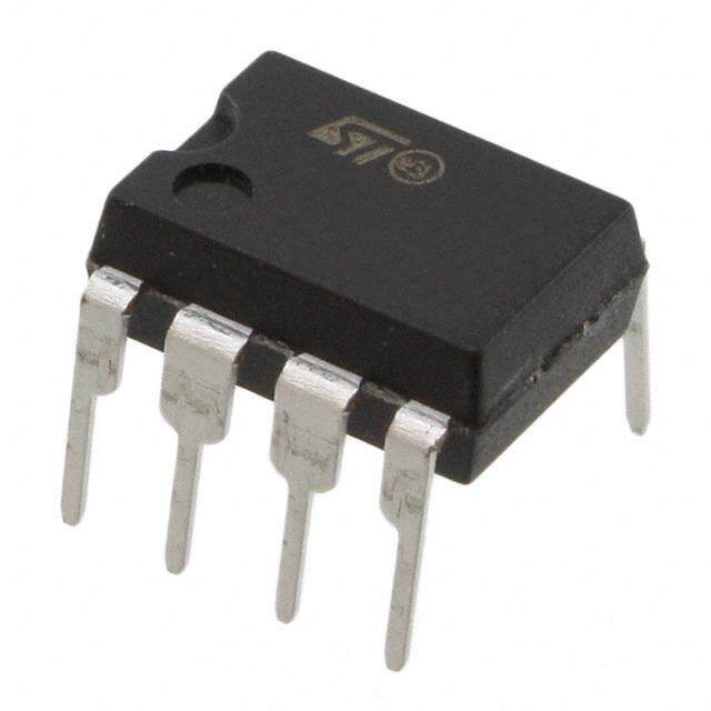
| 描述 | IC CTLR PWM CM OVP UVLO 8SOIC开关控制器 Quasi Resonant Current Mode PWM |
| 产品分类 | |
| 品牌 | ON Semiconductor |
| 产品手册 | |
| 产品图片 |
|
| rohs | 符合RoHS无铅 / 符合限制有害物质指令(RoHS)规范要求 |
| 产品系列 | 电源管理 IC,开关控制器 ,ON Semiconductor NCP1377DR2G- |
| 数据手册 | |
| 产品型号 | NCP1377DR2G |
| 上升时间 | 40 ns |
| 下降时间 | 20 ns |
| 产品种类 | 开关控制器 |
| 供应商器件封装 | 8-SOIC N |
| 其它名称 | NCP1377DR2GOSCT |
| 功率(W) | - |
| 包装 | 剪切带 (CT) |
| 商标 | ON Semiconductor |
| 安装风格 | SMD/SMT |
| 封装 | Reel |
| 封装/外壳 | 8-SOIC(0.154",3.90mm 宽) |
| 封装/箱体 | SOIC-8 Narrow |
| 工作温度 | -40°C ~ 125°C |
| 工厂包装数量 | 2500 |
| 开关频率 | 100 kHz |
| 拓扑结构 | Flyback |
| 最大工作温度 | + 150 C |
| 标准包装 | 1 |
| 电压-击穿 | - |
| 电压-输入 | 8.2 V ~ 18 V |
| 电压-输出 | - |
| 类型 | Current Mode PWM Controllers |
| 系列 | NCP1377 |
| 输出电压 | 18 V |
| 输出电流 | 500 mA |
| 输出端数量 | 1 Output |
| 输出隔离 | 隔离 |
| 频率范围 | 100kHz |


- 商务部:美国ITC正式对集成电路等产品启动337调查
- 曝三星4nm工艺存在良率问题 高通将骁龙8 Gen1或转产台积电
- 太阳诱电将投资9.5亿元在常州建新厂生产MLCC 预计2023年完工
- 英特尔发布欧洲新工厂建设计划 深化IDM 2.0 战略
- 台积电先进制程称霸业界 有大客户加持明年业绩稳了
- 达到5530亿美元!SIA预计今年全球半导体销售额将创下新高
- 英特尔拟将自动驾驶子公司Mobileye上市 估值或超500亿美元
- 三星加码芯片和SET,合并消费电子和移动部门,撤换高东真等 CEO
- 三星电子宣布重大人事变动 还合并消费电子和移动部门
- 海关总署:前11个月进口集成电路产品价值2.52万亿元 增长14.8%


PDF Datasheet 数据手册内容提取
NCP1377, NCP1377B PWM Current-Mode Controller for Free-Running Quasi-Resonant Operation The NCP1377 combines a true current mode modulator and a demagnetization detector which ensures full borderline/critical Conduction Mode in any load/line conditions together with www.onsemi.com minimum drain voltage switching (Quasi−Resonant operation). Due to its inherent skip cycle capability, the controller enters burst mode MARKING DIAGRAMS as soon as the power demand falls below a predetermined level. As this happens at low peak current, no audible noise can be heard. For 8 8 8 NCP1377, an internal 8.0 (cid:2)s timer prevents the free−run frequency to 1 1377 1377B ALYW ALYW exceed 100 kHz (therefore below the 150 kHz CISPR−22 EMI SOIC−8 (cid:2) (cid:2) starting limit), while the skip adjustment capability lets the user DR SUFFIX 1 1 select the frequency at which the burst foldback takes place. For CASE 751 NC1377B, the internal timer duration is reduced to 3.0 (cid:2)s to allow operation at higher frequencies (up to 300 kHz). The transformer core reset detection is done through an auxiliary 8 8 377D1 winding which, brought via a dedicated pin, also enables fast 1 ALYW(cid:2) Over Voltage Protection (OVP). Once an OVP has been detected, the SOIC−7 (cid:2) IC permanently latches off. The 1377 features a sampling time of D1 SUFFIX 1 4.5 (cid:2)s whereas it is 1.5 (cid:2)s for the B version. CASE 751U The NCP1377 also features an efficient protective circuitries which, in presence of an overcurrent condition, disables the output pulses and enters a safe burst mode, trying to restart. Once the default 1377P 1377BP has gone, the device auto−recovers. Finally an internal 1.0 ms AWL AWL 8 Soft−Start eliminates the traditional startup stress. YYWWG YYWWG 1 Features PDIP−7 1 1 • P SUFFIX Free−Running Borderline/Critical Mode Quasi−Resonant Operation CASE 626B • Latched Overvoltage Protection • Auto−Recovery Short−Circuit Protection Via UVLO Crossover A = Assembly Location • External Latch Triggering, e.g. Via Overtemperature Signal L, WL = Wafer Lot • Y, YY = Year Current−Mode with Adjustable Skip Cycle Capability W, WW = Work Week • Internal 1.0 ms Soft−Start (cid:2) or G = Pb−Free Package • (Note: Microdot may be in either location) Internal Temperature Shutdown • Internal Leading Edge Blanking • 500 mA Peak Current Source/Sink Capability PIN CONNECTIONS • Under Voltage Lockout Level of 12.5 V (On) and 7.5 V (Min) • Dmg 1 8 HV Direct Optocoupler Connection • SPICE Models Available for TRANsient Analysis FB 2 • Internal Minimum TOFF CS 3 6 VCC • These Devices are Pb−Free, Halogen Free/BFR Free and are RoHS GND 4 5 Drv Compliant (Top View) Typical Applications • AC−DC Adapters for Notebooks, etc. ORDERING INFORMATION • Offline Battery Chargers See detailed ordering and shipping information in the package • Consumer Electronics (DVD Players, Set−Top Boxes, TVs, etc.) dimensions section on page 14 of this data sheet. • Auxiliary Power Supplies (USB, Appliances, TVs, etc.) © Semiconductor Components Industries, LLC, 2015 1 Publication Order Number: October, 2015 − Rev. 13 NCP1377/D
NCP1377, NCP1377B R* 12 V @ 1 A + GND NCP1377 OVP and + Demag 1 8 Universal Network 2 7 3 6 4 5 + *Please refer to the application information section. Y1 Type Figure 1. Typical Application Schematic PIN FUNCTION DESCRIPTION Pin Symbol Function Description 1 Demag Core reset detection and OVP The auxiliary FLYBACK signal ensures discontinuous operation and offers a fixed overvoltage detection level of 7.2 V. 2 FB Sets the peak current setpoint By connecting an optocoupler to this pin, the peak current setpoint is adjusted accordingly to the output power demand. By bringing this pin below the internal skip level, you shut off the device. 3 CS Current sense input and skip This pin senses the primary current and routes it to the internal comparator via an cycle level selection L.E.B. By inserting a resistor in series with the pin, you control the level at which the skip operation takes place. 4 GND The IC ground − 5 Drv Driving pulses The driver’s output to an external MOSFET. 6 VCC Supplies the IC This pin is connected to an external bulk capacitor of typically 10 (cid:2)F. 7 NC − This unconnected pin ensures adequate creepage distance. 8 HV High−voltage pin Connected to the high−voltage rail, this pin injects a constant current into the VCC bulk capacitor and ensures a clean lossless startup sequence. www.onsemi.com 2
NCP1377, NCP1377B 1.5 us for B Version 4.5 us Delay Demag HV OVP Demag + 4 mA PON 8 us + 10 V Rint Blanking 50 mV 5 V /1.44 3 us for + B Version + S + Q VCC + S Q Drv VCC R R 12.5 V Driver src = 20 sink = 10 7.5 V 4.2 V 5.6 V (Fault) Fault To Internal Mngt. FB Supply + /3 - 1 V 200 (cid:2)A when DRV GND Overload? is OFF CS Time 380 ns 5 us Reset LEB Timeout Demag Figure 2. Internal Circuit Architecture MAXIMUM RATINGS Rating Symbol Value Unit Continuous Power Supply or Drive Voltage VCC, Drv 18 V Transient Power Supply Voltage, Duration < 10 ms, IVCC < 20 mA VCC Pulse 25 V Maximum Voltage on all other pins except Pin 8 (HV), Pin 6 (VCC) and Pin 5 (Drv) − −0.3 to 10 V Maximum Current into all pins except VCC (6), HV (8) and Demag (1) when 10 V ESD di- − 5.0 mA odes are activated Maximum Current in Pin 1 Idem +3.0/−2.0 mA Thermal Resistance, Junction−to−Case R(cid:3)JC 57 °C/W Thermal Resistance, Junction−to−Air, SOIC Version R(cid:3)JA 178 °C/W Thermal Resistance, Junction−to−Air, PDIP Version R(cid:3)JA 100 °C/W Maximum Junction Temperature TJMAX 150 °C Temperature Shutdown − 155 °C Hysteresis in Shutdown − 30 °C Storage Temperature Range − −60 to +150 °C ESD Capability, HBM Model (All pins except VCC and HV) − 2.0 kV ESD Capability, Machine Model − 200 V Maximum Voltage on Pin 8 (HV), Pin 6 (VCC) Decoupled to Ground with 10 (cid:2)F VHV 500 V Stresses exceeding those listed in the Maximum Ratings table may damage the device. If any of these limits are exceeded, device functionality should not be assumed, damage may occur and reliability may be affected. www.onsemi.com 3
NCP1377, NCP1377B ELECTRICAL CHARACTERISTICS (For typical values TJ = 25°C, for min/max values TJ = −40°C to +125°C, Max TJ = 150°C, VCC = 11 V unless otherwise noted.) Characteristic Pin Symbol Min Typ Max Unit SUPPLY SECTION VCC Increasing Level at which the Current Source Turns−Off 6 VCCON 11.6 12.5 13.7 V Minimum Operating Voltage after Turn−On 6 VCCOFF 7.0 7.5 8.2 V VCC Decreasing Level at which the Latchoff Phase Ends 6 VCClatch − 5.6 − V Internal IC Consumption, No Output Load on Pin 5, FSW = 60 kHz 6 ICC1 − 1.0 1.3 mA (Note 1) Internal IC Consumption, 1.0 nF Output Load on Pin 5, FSW = 60 kHz 6 ICC2 − 1.6 2.0 mA (Note 1) Internal IC Consumption, Latchoff Phase, VCC = 6.0 V 6 ICC3 − 220 − (cid:2)A INTERNAL STARTUP CURRENT SOURCE High−Voltage Current Source, VCC = 10 V, Vpin8 = 50 V 8 IC1 2.4 4.0 6.0 mA High−Voltage Current Source, VCC = 0 V, Vpin8 = 50 V 8 IC2 − 4.5 − mA Startup Leakage, Vpin8 = 500 V 8 IHVLeak − 30 70 (cid:2)A High Voltage Minimum Startup, VCC = VCC(on)−0.2 V, ICC = 1 mA 8 HVmin − 20 23.5 V DRIVE OUTPUT Output Voltage Rise−Time @ CL = 1.0 nF, 10−90% of Output Signal 5 Tr − 40 − ns Output Voltage Fall−Time @ CL = 1.0 nF, 10−90% of Output Signal 5 Tf − 20 − ns Source Resistance 5 ROH 12 20 36 (cid:4) Sink Resistance 5 ROL 5.0 10 19 (cid:4) CURRENT COMPARATOR Input Bias Current @ 1.0 V Input Level on Pin 3 3 IIB − 0.02 − (cid:2)A Maximum Internal Current Setpoint 3 ILimit 0.9 1.0 1.1 V Propagation Delay from Current Detection to Gate OFF State 3 TDEL − 100 160 ns Leading Edge Blanking Duration 3 TLEB − 380 − ns Internal Current Offset Injected on the CS Pin During OFF Time 3 Iskip − 200 − (cid:2)A OVERVOLTAGE SECTION Sampling Delay After ON Time NCP1377 1 Tsample − 4.5 − (cid:2)s NCP1377B 1 − 1.5 − OVP Internal Reference Level 1 Vref 6.4 7.2 8.0 V FEEDBACK SECTION Internal Pullup Resistor 2 Rup − 20 − k(cid:4) Pin 3 to Current Setpoint Division Ratio − Iratio − 3.3 − − Internal Soft−Start − Tss − 1.0 − ms DEMAGNETIZATION DETECTION BLOCK Input Threshold Voltage (Vpin 1 Decreasing) 1 Vth 35 50 90 mV Hysteresis (Vpin 1 Decreasing) 1 VH − 20 − mV Input Clamp Voltage V High State (Ipin 1 = 3.0 mA) 1 VCH 8.0 10 12 Low State (Ipin 1 = −2.0 mA) 1 VCL −0.9 −0.7 −0.5 Pin1 Internal Resistance 1 Rint − 28 − k(cid:4) Demag Propagation Delay 1 Tdem − 210 − ns Timeout After Last Demag Transition 1 Tout − 5.0 − (cid:2)s Internal Input Capacitance at Vpin 1 = 1.0 V 1 Cpar − 10 − pF Minimum TOFF (Internal Blanking Delay After TON) NCP1377 1 Tblank − 8.0 − (cid:2)s NCP1377B 1 − 3.0 − 1. Max value at Tj = −40°C, please see characterization curves. www.onsemi.com 4
NCP1377, NCP1377B TYPICAL CHARACTERISTICS 14.0 7.90 7.80 13.5 7.70 13.0 , (V)ON 12.5 , (V)OFF 7.60 C C 7.50 C C V V 12.0 7.40 11.5 7.30 11.0 7.20 −50 −30 −10 10 30 50 70 90 110 130 −50 −30 −10 10 30 50 70 90 110 130 TEMPERATURE (°C) TEMPERATURE (°C) Figure 3. VCCON Threshold versus Temperature Figure 4. VCCOFF Threshold versus Temperature 1.60 2.30 1.40 2.10 1.20 1.90 A) A) m m , (1 1.00 , (2 1.70 C C C C I I 0.80 1.50 0.60 1.30 0.40 1.10 −50 −30 −10 10 30 50 70 90 110 130 −50 −30 −10 10 30 50 70 90 110 130 TEMPERATURE (°C) TEMPERATURE (°C) Figure 5. Current Consumption (No Load) Figure 6. Current Consumption (1.0 nF Load) versus Temperature versus Temperature 6.0 1.10 5.5 5.0 1.05 4.5 A) V) I, (mC1 34..50 I, (limit 1.00 3.0 0.95 2.5 2.0 0.90 −50 −30 −10 10 30 50 70 90 110 130 −50 −30 −10 10 30 50 70 90 110 130 TEMPERATURE (°C) TEMPERATURE (°C) Figure 7. HV Current Source at VCC = 10 V Figure 8. Maximum Current Setpoint versus versus temperature Temperature www.onsemi.com 5
NCP1377, NCP1377B TYPICAL CHARACTERISTICS 40.0 20.0 35.0 18.0 16.0 30.0 14.0 25.0 (cid:4)) (cid:4)) 12.0 , (H 20.0 , (L 10.0 O O R R 8.0 15.0 6.0 10.0 4.0 5.0 2.0 0.0 0.0 −50 −30 −10 10 30 50 70 90 110 130 −50 −30 −10 10 30 50 70 90 110 130 TEMPERATURE (°C) TEMPERATURE (°C) Figure 9. Drive Source Resistance versus Figure 10. Drive Sink Resistance versus Temperature Temperature 120 7.8 7.6 100 7.4 80 mV) V) 7.2 , (TH 60 V, (ref 7.0 V 40 6.8 20 6.6 0 6.4 −50 −30 −10 10 30 50 70 90 110 130 −50 −30 −10 10 30 50 70 90 110 130 TEMPERATURE (°C) TEMPERATURE (°C) Figure 11. Demagnetization Detection Threshold Figure 12. OVP Threshold versus Temperature versus Temperature 10.0 7.30 9.5 6.80 9.0 6.30 (cid:2)s) 8.5 s) 5.80 , (blank 8.0 (cid:2)T, (out 5.30 T 7.5 4.80 7.0 4.30 6.5 3.80 −50 −30 −10 10 30 50 70 90 110 130 −50 −30 −10 10 30 50 70 90 110 130 TEMPERATURE (°C) TEMPERATURE (°C) Figure 13. Minimum T versus Temperature Figure 14. Demagnetization Detection Timeout OFF versus Temperature www.onsemi.com 6
NCP1377, NCP1377B 60 NCP1377 goes into latched fault condition whenever an overvoltage condition is detected. The controller 50 stays fully latched in this position until the Vcc is cycled down to 4.0 V, e.g. when the user unplugs the 40 power supply from the mains outlet and replugs it. • (cid:4) External Latch Trip Point: By externally forcing a knt30 level on the OVP greater than the internal setpoint, it Ri is possible to latchoff the IC, e.g. with a signal coming 20 from a temperature sensor. • Adjustable Skip Cycle Level: By offering the ability 10 to tailor the level at which the skip cycle takes place, the designer can make sure that the skip operation 0 −50 −30 −10 10 30 50 70 90 110 130 only occurs at low peak current. This point guarantees a noise−free operation with cheap transformer. This TEMPERATURE (°C) option also offers the ability to fix the maximum Figure 15. DMG Pin Internal Resistance versus switching frequency when entering light load conditions. Temperature • Overcurrent Protection (OCP): NCP1377 enters burst mode as soon as the power supply undergoes an overload which is detected through the sense of the APPLICATION INFORMATION auxiliary voltage. As detailed above, as soon as Vcc INTRODUCTION crosses the undervoltage lockout level (VCCoff in the electrical table), all pulses are stopped and the device The NCP1377 implements a standard current mode enters a safe low power operation which prevents from architecture where the switch−off time is dictated by the any lethal thermal runaway. By monitoring the Vcc peak current setpoint, whereas the core reset detection level, the startup current source is activated ON and triggers the turn−on event. This component represents the OFF to create a kind of burst mode where the SMPS ideal candidate where low part−count is the key parameter, tries to restart. If the fault has gone, the SMPS particularly in low−cost AC−DC adapters, consumer resumes operation. On the other hand, if the fault is electronics, auxiliary supplies, etc. Due to its high− still there, the burst sequence starts again. performance high−voltage technology, the NCP1377 incorporates all the necessary components/features needed Startup Sequence to build a rugged and reliable Switchmode Power Supply When the power supply is first powered from the mains (SMPS): outlet, the internal current source (typically 4.0 mA) is • Transformer Core Reset Detection: Borderline/critical biased and charges up the Vcc capacitor. When the voltage operation is ensured whatever the operating conditions on this Vcc capacitor reaches the Vcc level (typically ON are. As a result, there are virtually no primary switch 12.5 V), the current source turns off and no longer wastes turn−on losses and no secondary diode recovery any power. At this time, the Vcc capacitor only supplies the losses. The converter also stays a first−order system controller and the auxiliary supply is supposed to take over and accordingly eases the feedback loop design. before Vcc collapses below V . Figure 16 shows the CCoff • Quasi−Resonant Operation: By delaying the turn−on internal arrangement of this structure. event, it is possible to restart the MOSFET in the minimum of the drain−source wave, ensuring reduced 8 HV EMI/video noise perturbations. In nominal power VccON/VccOFF + IC1 or 0 − conditions, the NCP1377 operates in Borderline Conduction Mode (BCM) also called Critical 6 Conduction Mode. • Undervoltage Lockout (UVLO): When Vcc falls below CVCC Aux V pulses are stopped and the IC consumption CCoff 4 drops down to a few hundred of (cid:2)A. When Vcc reaches the latchoff level (5.6 V typical), the startup Figure 16. The Current Source Brings Vcc Above current source is activated and brings Vcc back to Vcc and Then Turns Off ON Vcc where the IC attempts to startup. on • Overvoltage Protection (OVP): By sampling the plateau voltage on the demagnetization winding, the www.onsemi.com 7
NCP1377, NCP1377B Once the power supply has started, the V shall be Skipping Cycle Mode CC constrained below 18 V, which is the maximum rating on The NCP1377 automatically skips switching cycles pin 6. Figure 17 portrays a typical NCP1377 startup when the output power demand drops below a given level. sequence with a Vcc regulated at 12.5 V. This is accomplished by monitoring the FB pin. In normal operation, pin 2 imposes a peak current accordingly to the load value. If the load demand decreases, the internal loop 13.5 asks for less peak current. When this setpoint reaches a determined level, the IC prevents the current from 12.5 V Regulation 12.5 decreasing further down and starts to blank the output pulses: the IC enters the so−called skip cycle mode, also named controlled burst operation. The power transfer now C11.5 C depends upon the width of the pulse bunches (Figure 18) V and follows the following formula: 10.5 1 ·Lp·Ip2·Fsw·Dburst with: 2 Lp = Primary inductance 9.50 Fsw = Switching frequency within the burst Ip = Peak current at which skip cycle occurs Figure 17. A Typical Startup Sequence D = Burst width/burst recurrence burst for the NCP1377 DRIVER MAX PEAK NORMAL CURRENT V)300 CURRENT MODE OPERATION DRIVER = HIGH ? I = 0 m L ( DRIVER = LOW ? I = 200 (cid:2)A A E SIGN200 CUSRKRIPE CNYTC LLIMEIT RESET +- 3 Rskip S100 N Rsense SE 2 T N 0 E R WIDTH R + U C RECURRENCE Figure 18. The Skip Cycle Takes Place at Low Peak Figure 19. A Patented Method Allows for Skip Currents which Guarantees Noise−Free Operation Level Selection via a Series Resistor Inserted in Series with the Current The skip level selection is done through a simple resistor voltage is below Rskip level, then the current sense inserted between the current sense input and the sense comparator permanently resets the latch and the next clock element. Everytime the NCP1377 output driver goes low, cycle (given by the demagnetization detection) is ignored: a 200 (cid:2)A source forces a current to flow through the sense we are skipping cycles as shown by Figure 18. As soon as pin (Figure 19): when the driver is high, the current source the feedback voltage goes up again, there can be two is off and the current sense information is normally situations: the recurrent period is small and a new processed. As soon as the driver goes low, the current demagnetization detection (next wave) signal triggers the source delivers 200 (cid:2)A and develops a ground referenced NCP1377. To the opposite, in low output power conditions, voltage across Rskip. If this voltage is below the feedback no more ringing waves are present on the drain and the voltage, the current sense comparator stays in the low state toggling of the current sense comparator alone initiates a and the internal latch can be triggered by the next clock new cycle start. Figure 20 depicts these two different cycle. Now, if because of a low load mode the feedback situations. www.onsemi.com 8
NCP1377, NCP1377B Drain Signal Timeout Signal Demag Restart Current Sense and Timeout Restart Drain Signal Timeout 5 (cid:2)s 5 (cid:2)s Signal Figure 20. When the primary natural ringing becomes too low, the internal TimeOut together with the sense comparator initiates a new cycle when FB passes the skip level. An optocoupler is generally used to transfer the feedback maximum peak current). If anyway a lower skip threshold information to the FB pin while providing the necessary is needed, care must be taken to select an optocoupler with isolation. It introduces a limitation in how low the skip a Vce(sat) guaranteed to be below the chosen skip level level can be adjusted since an optocoupler cannot pull the with enough margin. FB voltage below its Vce(sat), which is usually around Demagnetization Detection 150 mV. Therefore, in order to take into account The core reset detection is done by monitoring the temperature and process variations, it is not recommended voltage activity on the auxiliary winding. This voltage to set up the skip level below 250 mV, which corresponds to a minimum resistor Rskip of 420 (cid:4). The 150 mV is a features a FLYBACK polarity. The typical detection level is fixed at 50 mV as exemplified by Figure 21. much lower level than what will usually be used (it sets the peak current when entering skip mode at 5% of the 7.0 V) 5.0 POSSIBLE L ( RESTARTS A TO INTERNAL N G SIG 3.0 COMPARATOR 2 Resd 1 1 5Rdem 4 A M DE 1.0 50 mV Rint ESD2 ESD1 Aux 0 V −1.0 4 3 Resd + Rint = 28 k Figure 21. Core Reset Detection is Done through Figure 22. Internal Pad Implementation a Dedicated Auxiliary Winding Monitoring www.onsemi.com 9
NCP1377, NCP1377B An internal timer prevents any restart within 8.0 (cid:2)s for NCP1377 and 1.5 (cid:2)s for NCP1377B guarantees a clean further to the driver going−low transition for NCP1377, plateau, providing that the leakage inductance ringing has and 3.0 (cid:2)s for NCP1377B. This prevents the switching been fully damped. If this would not be the case, the frequency to exceed (1.0/T + T ) but also avoid false designer should install a small RC damper across the ON blank leakage inductance tripping at turn−off. In some cases, the transformer primary inductance connections. Figure 24 leakage inductance kick is so energetic, that a slight shows where the sampling occurs on the auxiliary winding. filtering is necessary. The NCP1377 demagnetization detection pad features a specific component arrangement as detailed by Figure 22. SAMPLING HERE 8.0 In this picture, the zener diodes network protect the IC against any potential ESD discharge that could appear on the pins. The first ESD diode connected to the pad, exhibits L (V) 6.0 a parasitic capacitance. When this parasitic capacitance A N (10 pF typically) is combined with Rdem, a restart delay G SI 4.0 is created and the possibility to switch right in the G drain−source wave exists. This guarantees QR operation MA with all the associated benefits (low EMI, no turn−on DE 2.0 losses etc.). Rdem should be calculated to limit the 4.5 (cid:2)s maximum current flowing through pin 1 to less than 0 +3.0 mA/−2.0 mA: If during turn−on, the auxiliary winding delivers 30 V (at the highest line level), then the minimum Rdem value is defined by: 30 + 0.7/3.0 mA = Figure 24. A Voltage Sample is Taken 4.5 (cid:2)s 10.2 k(cid:4). This value will be further increased, e.g. to After the Turn−Off Sequence introduce a restart delay and also a slight filtering in case When an OVP condition has been detected, the of high leakage energy. NCP1377 enters a latchoff phase and stops all switching Figure 23 portrays a typical Vds shot at nominal output operations. The controller stays fully latched in this power. position and the startup source being still active, it keeps the Vcc going up and down between 12.5 V and 5.6 V. This state lasts until the Vcc is cycled down to 4.0 V, e.g. when 400 the user unplugs the power supply from the mains outlet. V) By default, the OVP comparator is biased to a 5.0 V E (300 reference level and pin1 is routed via a divide by a 1.44 G A network. As a result, when Vpin1 reaches 7.2 V, the OVP T OL200 comparator is triggered. The threshold can thus be adjusted V by either modifying the power winding to auxiliary N AI winding turn ratios to match this 7.2 V level or insert a R100 D resistor from pin1 to ground to cope with your design requirement. 0 Latching Off the NCP1377 In certain cases, it can be very convenient to externally Figure 23. The NCP1377 Operates in shut down permanently the NCP1377 via a dedicated Borderline/Critical Operation signal, e.g. coming from a temperature sensor (Figure 25). The reset occurs when the user unplugs the power supply Overvoltage Protection from the mains outlet. To trigger the latchoff by an external The overvoltage protection works by sampling the signal, a simple PNP transistor can do the work, as plateau voltage after the turn−off sequence. A 4.5 (cid:2)s delay Figure 26 shows. www.onsemi.com 10
NCP1377, NCP1377B Thermistor Rdem NCP1377 Aux. 1 8 1 8 Aux. 2 7 2 7 Winding 3 6 ON/OFF 3 6 4 5 4 5 CVCC VCCcap Figure 25. A simple arrangement triggers Figure 26. A simple transistor arrangement the latchoff as soon as the temperature triggers the latchoff as soon as the exceeds a given setpoint. temperature exceeds a given setpoint. Shutting Off the NCP1377 a low level, preventing a bias current to circulate in the Shutdown can easily be implemented through a simple optocoupler LED. As a result, the auxiliary voltage also NPN bipolar transistor as depicted by Figure 27. When decreases because it also operates in Flyback and thus OFF, Q1 is transparent to the operation. When forward duplicates the output voltage, providing the leakage biased, the transistor pulls the FB pin to ground (Vcesat ≈ inductance between windings is kept low. To account for 200 mV) and permanently disables the IC. A small time this situation and properly protect the power supply, constant on the transistor base will avoid false triggering NCP1377 hosts a dedicated overload detection circuitry. (Figure 27). Once activated, this circuitry imposes to deliver pulses in a burst manner with a low Duty Cycle. The system NCP1377 auto−recovers when the fault condition disappears. During the startup phase, the peak current is pushed to 1 8 the maximum until the output voltage reaches its target and 2 7 the feedback loop takes over. The auxiliary voltage takes 1 10 k place after a few switching cycles and self−supplies the IC. 3 6 ON/OFF Q1 In presence of a short circuit on the output, the auxiliary 3 2 4 5 10 nF voltage will go down until it crosses the undervoltage lockout level of typically 7.5 V. When this happens, NCP1377 immediately stops the switching pulses and unbiases all unnecessary logical blocks. The overall consumption drops, while keeping the gate grounded, and Figure 27. A Simple Bipolar Transistor Totally Disables the IC the Vcc slowly falls down. As soon as Vcc reaches typically 5.6 V, the startup source turns−on again and a new startup Overload Operation sequence occurs, bringing Vcc toward 12.5 V as an attempt In applications where the output current is purposely not to restart. If the default has gone, then the power supply controlled (e.g. wall adapters delivering raw DC level), it normally restarts. If not, a new protective burst is initiated, is interesting to implement a true short−circuit protection. shielding the SMPS from any runaway. Figure 28 portrays A short−circuit actually forces the output voltage to be at the typical operating signals in short circuit. www.onsemi.com 11
NCP1377, NCP1377B VccON Vccoff Vcc Vcclatch Driving Pulses Figure 28. Typical Waveforms in Short Circuit Conditions Soft−Start (cid:5)t·i The NCP1377 features an internal 1.0 ms Soft−Start to 15 ms. CVCC is calculated using the equation C(cid:2) (cid:5)V or soften the constraints occurring in the power supply during C(cid:3)8.6(cid:2)F. Select a 22 (cid:2)F/16 V and this will fit. During startup. It is activated during the power on sequence. As the latchoff phase, the current consumption drops to ICC3 soon as Vcc reaches Vcc , the peak current is gradually or 220 (cid:2)A. We can now calculate how long this latchoff ON increased from nearly zero up to the maximum clamping phase will last: (7.5–5.6) x 22 (cid:2)/220 u = 190 ms. level (e.g. 1.0 V). The Soft−Start is also activated during Protecting Pin 8 Against Negative Spikes the overcurrent burst (OCP) sequence. Every restart As any CMOS controller, NCP1377 is sensitive to attempt is followed by a Soft−Start activation. Generally negative voltages that could appear on its pins. To avoid speaking, the Soft−Start will be activated when Vcc ramps any adverse latchup of the IC, we strongly recommend to up either from zero (fresh power−on sequence) or 5.6 V, the insert a resistor R in series with pin8. This resistor latchoff voltage occurring during OCP. HV prevents from adversely latching the controller in case of Calculating the Vcc Capacitor negative spikes appearing on the bulk capacitor during the The Vcc capacitor can be calculated knowing the IC power−off sequence. A typical value of 6.8 k(cid:4)/0.5 W is consumption as soon as Vcc reaches Vcc . Suppose that suitable. This resistor does not dissipate any power since it ON a NCP1377 is used and drives a MOSFET with a 30 nC only sees current during the startup sequence and during total gate charge (Qg). The total average current is thus overload. Calculations actually involve the minimum made of Icc1 (1.0 mA) plus the driver current, Fsw x Qg or voltage on pin8 necessary to fully activate the current 1.8 mA. The total current is therefore 2.8 mA. The (cid:5)V source. This minimum voltage being 40 V, therefore RHV available to fully startup the circuit (e.g. never reach the shall be less than: (Vbulkmin–40)/6.0 m. 7.5 V UVLO during power on) is 12.5 – 7.5 = 5.0 V. We Operating Shots have a capacitor which then needs to supply the NCP1377 Following are some oscilloscope shots captured at with 2.8 mA during a given time until the auxiliary supply Vin = 120 VDC with a transformer featuring a 800 (cid:2)H takes over. Suppose that this time was measured at around primary inductance. www.onsemi.com 12
NCP1377, NCP1377B Figure 29. This plot gathers waveforms captured at three different operating points: 1st Upper Plot: Free run, valley switching operation, Pout = 26 W. 2nd Middle Plot: Min Toff clamps the switching frequency and selects the second valley. 3rd Lowest Plot: The skip slices the second valley pattern and will further expand the burst as Pout goes low. Vrsense (200 mV/div) Vgate (5 V/div) 200 (cid:2)A x Rskip Current Sense Pin (200 mV/pin) Figure 30. This picture explains how the 200 (cid:2)A internal offset current creates the skip cycle level. www.onsemi.com 13
NCP1377, NCP1377B Vcc (5 V/div) Vgate (5 V/div) Latchoff Level Figure 31. The short−circuit protection forces the IC to enter burst in presence of a secondary overload. ORDERING INFORMATION Device Package Type Shipping† NCP1377DR2G SOIC−8 2500 / Tape & Reel (Pb−Free) NCP1377BDR2G SOIC−8 2500 / Tape & Reel (Pb−Free) NCP1377D1R2G SOIC−7 2500 / Tape & Reel (Pb−Free) NCP1377BD1R2G SOIC−7 2500 / Tape & Reel (Pb−Free) NCP1377PG PDIP−7 50 Units / Rail (Pb−Free) NCP1377BPG PDIP−7 50 Units / Rail (Pb−Free) †For information on tape and reel specifications, including part orientation and tape sizes, please refer to our Tape and Reel Packaging Specifications Brochure, BRD8011/D. www.onsemi.com 14
NCP1377, NCP1377B PACKAGE DIMENSIONS PDIP−7 (PDIP−8 LESS PIN 7) P SUFFIX CASE 626B ISSUE D D A NOTES: 1. DIMENSIONING AND TOLERANCING PER ASME Y14.5M, 1994. E 2. CONTROLLING DIMENSION: INCHES. H 3. DIMENSIONS A, A1 AND L ARE MEASURED WITH THE PACK- AGE SEATED IN JEDEC SEATING PLANE GAUGE GS−3. 8 5 4. DIMENSIONS D, D1 AND E1 DO NOT INCLUDE MOLD FLASH OR PROTRUSIONS. MOLD FLASH OR PROTRUSIONS ARE NOT E1 TO EXCEED 0.10 INCH. 5. DIMENSION E IS MEASURED AT A POINT 0.015 BELOW DATUM 1 4 PLANE H WITH THE LEADS CONSTRAINED PERPENDICULAR TO DATUM C. 6. DIMENSION eB IS MEASURED AT THE LEAD TIPS WITH THE NOTE 8 c LEADS UNCONSTRAINED. b2 B 7. DATUM PLANE H IS COINCIDENT WITH THE BOTTOM OF THE END VIEW LEADS, WHERE THE LEADS EXIT THE BODY. TOP VIEW WITH LEADS CONSTRAINED 8. PACKAGE CONTOUR IS OPTIONAL (ROUNDED OR SQUARE CORNERS). NOTE 5 INCHES MILLIMETERS A2 DIM MIN MAX MIN MAX e/2 A −−−− 0.210 −−− 5.33 A NOTE 3 A1 0.015 −−−− 0.38 −−− A2 0.115 0.195 2.92 4.95 L b 0.014 0.022 0.35 0.56 b2 0.060 TYP 1.52 TYP C 0.008 0.014 0.20 0.36 D 0.355 0.400 9.02 10.16 SEATING A1 PLANE DE1 00..030050 0−.−3−2−5 07..1632 8−.−2−6 C M E1 0.240 0.280 6.10 7.11 D1 e 0.100 BSC 2.54 BSC e eB eB −−−− 0.430 −−− 10.92 L 0.115 0.150 2.92 3.81 8Xb END VIEW M −−−− 10° −−− 10° 0.010 M C A M B M NOTE 6 SIDE VIEW www.onsemi.com 15
NCP1377, NCP1377B SOIC−7 CASE 751U ISSUE E −A− NOTES: 1. DIMENSIONING AND TOLERANCING PER ANSI Y14.5M, 1982. 2. CONTROLLING DIMENSION: MILLIMETER. 8 5 3. DIMENSION A AND B ARE DATUMS AND T IS A DATUM SURFACE. −B− S 0.25 (0.010) M B M 4. DIMENSION A AND B DO NOT INCLUDE MOLD PROTRUSION. 1 5. MAXIMUM MOLD PROTRUSION 0.15 (0.006) 4 PER SIDE. MILLIMETERS INCHES DIM MIN MAX MIN MAX G A 4.80 5.00 0.189 0.197 B 3.80 4.00 0.150 0.157 C RX 45(cid:3) C 1.35 1.75 0.053 0.069 D 0.33 0.51 0.013 0.020 J G 1.27 BSC 0.050 BSC −T− H 0.10 0.25 0.004 0.010 SEATING J 0.19 0.25 0.007 0.010 PLANE K K 0.40 1.27 0.016 0.050 H D7 PL M MN 0.205 (cid:3) 0.580 (cid:3) 0.0100 (cid:3) 0.0280 (cid:3) S 5.80 6.20 0.228 0.244 0.25 (0.010)M T B S A S SOLDERING FOOTPRINT* 1.52 0.060 7.0 4.0 0.275 0.155 0.6 1.270 0.024 0.050 (cid:4) (cid:5) mm SCALE 6:1 inches *For additional information on our Pb−Free strategy and soldering details, please download the ON Semiconductor Soldering and Mounting Techniques Reference Manual, SOLDERRM/D. www.onsemi.com 16
NCP1377, NCP1377B PACKAGE DIMENSIONS SOIC−8 DR SUFFIX CASE 751−07 ISSUE AK NOTES: −X− 1. DIMENSIONING AND TOLERANCING PER ANSI Y14.5M, 1982. A 2. CONTROLLING DIMENSION: MILLIMETER. 3. DIMENSION A AND B DO NOT INCLUDE MOLD PROTRUSION. 4. MAXIMUM MOLD PROTRUSION 0.15 (0.006) 8 5 PER SIDE. 5. DIMENSION D DOES NOT INCLUDE DAMBAR B S 0.25 (0.010) M Y M PROTRUSION. ALLOWABLE DAMBAR PROTRUSION SHALL BE 0.127 (0.005) TOTAL 1 IN EXCESS OF THE D DIMENSION AT −Y− 4 K 6. M75A1X−I0M1U TMH RMUA T7E51R−IA06L CAROEN DOIBTSIOONL.ETE. NEW STANDARD IS 751−07. G MILLIMETERS INCHES DIM MIN MAX MIN MAX A 4.80 5.00 0.189 0.197 C NX 45(cid:3) B 3.80 4.00 0.150 0.157 SEATING C 1.35 1.75 0.053 0.069 PLANE D 0.33 0.51 0.013 0.020 −Z− G 1.27 BSC 0.050 BSC H 0.10 0.25 0.004 0.010 0.10 (0.004) J 0.19 0.25 0.007 0.010 H D M J K 0.40 1.27 0.016 0.050 M 0 (cid:3) 8 (cid:3) 0 (cid:3) 8 (cid:3) 0.25 (0.010)M Z Y S X S N 0.25 0.50 0.010 0.020 S 5.80 6.20 0.228 0.244 SOLDERING FOOTPRINT* 1.52 0.060 7.0 4.0 0.275 0.155 0.6 1.270 0.024 0.050 (cid:4) (cid:5) mm SCALE 6:1 inches *For additional information on our Pb−Free strategy and soldering details, please download the ON Semiconductor Soldering and Mounting Techniques Reference Manual, SOLDERRM/D. ON Semiconductor and the are registered trademarks of Semiconductor Components Industries, LLC (SCILLC) or its subsidiaries in the United States and/or other countries. SCILLC owns the rights to a number of patents, trademarks, copyrights, trade secrets, and other intellectual property. A listing of SCILLC’s product/patent coverage may be accessed at www.onsemi.com/site/pdf/Patent−Marking.pdf. SCILLC reserves the right to make changes without further notice to any products herein. SCILLC makes no warranty, representation or guarantee regarding the suitability of its products for any particular purpose, nor does SCILLC assume any liability arising out of the application or use of any product or circuit, and specifically disclaims any and all liability, including without limitation special, consequential or incidental damages. “Typical” parameters which may be provided in SCILLC data sheets and/or specifications can and do vary in different applications and actual performance may vary over time. All operating parameters, including “Typicals” must be validated for each customer application by customer’s technical experts. SCILLC does not convey any license under its patent rights nor the rights of others. SCILLC products are not designed, intended, or authorized for use as components in systems intended for surgical implant into the body, or other applications intended to support or sustain life, or for any other application in which the failure of the SCILLC product could create a situation where personal injury or death may occur. Should Buyer purchase or use SCILLC products for any such unintended or unauthorized application, Buyer shall indemnify and hold SCILLC and its officers, employees, subsidiaries, affiliates, and distributors harmless against all claims, costs, damages, and expenses, and reasonable attorney fees arising out of, directly or indirectly, any claim of personal injury or death associated with such unintended or unauthorized use, even if such claim alleges that SCILLC was negligent regarding the design or manufacture of the part. SCILLC is an Equal Opportunity/Affirmative Action Employer. This literature is subject to all applicable copyright laws and is not for resale in any manner. PUBLICATION ORDERING INFORMATION LITERATURE FULFILLMENT: N. American Technical Support: 800−282−9855 Toll Free ON Semiconductor Website: www.onsemi.com Literature Distribution Center for ON Semiconductor USA/Canada 19521 E. 32nd Pkwy, Aurora, Colorado 80011 USA Europe, Middle East and Africa Technical Support: Order Literature: http://www.onsemi.com/orderlit Phone: 303−675−2175 or 800−344−3860 Toll Free USA/Canada Phone: 421 33 790 2910 Fax: 303−675−2176 or 800−344−3867 Toll Free USA/Canada Japan Customer Focus Center For additional information, please contact your local Email: orderlit@onsemi.com Phone: 81−3−5817−1050 Sales Representative www.onsemi.com NCP1377/D 17