ICGOO在线商城 > 集成电路(IC) > PMIC - AC-DC 转换器,离线开关 > NCP1200D100R2G

 Datasheet下载
- 型号: NCP1200D100R2G
- 制造商: ON Semiconductor
- 库位|库存: xxxx|xxxx
- 要求:
| 数量阶梯 | 香港交货 | 国内含税 |
| +xxxx | $xxxx | ¥xxxx |
查看当月历史价格
查看今年历史价格
NCP1200D100R2G产品简介:
ICGOO电子元器件商城为您提供NCP1200D100R2G由ON Semiconductor设计生产,在icgoo商城现货销售,并且可以通过原厂、代理商等渠道进行代购。 NCP1200D100R2G价格参考。ON SemiconductorNCP1200D100R2G封装/规格:PMIC - AC-DC 转换器,离线开关, Converter Offline Flyback Topology 100kHz 8-SOIC。您可以下载NCP1200D100R2G参考资料、Datasheet数据手册功能说明书,资料中有NCP1200D100R2G 详细功能的应用电路图电压和使用方法及教程。
| 参数 | 数值 |
| 产品目录 | 集成电路 (IC)半导体 |
| 描述 | IC CTRLR PWM CM 8SOIC开关控制器 100KHz Current Mode SMPS PWM |
| 产品分类 | |
| 品牌 | ON Semiconductor |
| 产品手册 | |
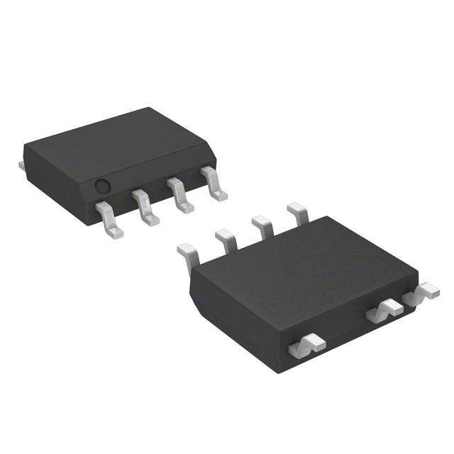
| 产品图片 |
|
| rohs | 符合RoHS无铅 / 符合限制有害物质指令(RoHS)规范要求 |
| 产品系列 | 电源管理 IC,开关控制器 ,ON Semiconductor NCP1200D100R2G- |
| 数据手册 | |
| 产品型号 | NCP1200D100R2G |
| 上升时间 | 67 ns |
| 下降时间 | 28 ns |
| 产品种类 | 开关控制器 |
| 供应商器件封装 | 8-SOIC N |
| 其它名称 | NCP1200D100R2GOSCT |
| 功率(W) | - |
| 包装 | 剪切带 (CT) |
| 占空比-最大 | 80 % |
| 商标 | ON Semiconductor |
| 安装风格 | SMD/SMT |
| 封装 | Reel |
| 封装/外壳 | 8-SOIC(0.154",3.90mm 宽) |
| 封装/箱体 | SOIC-8 Narrow |
| 工作温度 | -25°C ~ 125°C |
| 工作电源电压 | 16 V |
| 工厂包装数量 | 2500 |
| 开关频率 | 103 kHz |
| 拓扑结构 | Flyback, Forward |
| 最大工作温度 | + 150 C |
| 标准包装 | 1 |
| 电压-击穿 | - |
| 电压-输入 | 11 V ~ 16 V |
| 电压-输出 | - |
| 类型 | Current Mode PWM Controllers |
| 系列 | NCP1200 |
| 输出电流 | 250 mA |
| 输出端数量 | 1 Output |
| 输出隔离 | 隔离 |
| 频率范围 | 86kHz ~ 116kHz |


- 商务部:美国ITC正式对集成电路等产品启动337调查
- 曝三星4nm工艺存在良率问题 高通将骁龙8 Gen1或转产台积电
- 太阳诱电将投资9.5亿元在常州建新厂生产MLCC 预计2023年完工
- 英特尔发布欧洲新工厂建设计划 深化IDM 2.0 战略
- 台积电先进制程称霸业界 有大客户加持明年业绩稳了
- 达到5530亿美元!SIA预计今年全球半导体销售额将创下新高
- 英特尔拟将自动驾驶子公司Mobileye上市 估值或超500亿美元
- 三星加码芯片和SET,合并消费电子和移动部门,撤换高东真等 CEO
- 三星电子宣布重大人事变动 还合并消费电子和移动部门
- 海关总署:前11个月进口集成电路产品价值2.52万亿元 增长14.8%


PDF Datasheet 数据手册内容提取
NCP1200 PWM Current-Mode Controller for Low-Power Universal Off-Line Supplies Housed in SOIC−8 or PDIP−8 package, the NCP1200 represents a major leap toward ultra−compact Switchmode Power Supplies. Due to www.onsemi.com a novel concept, the circuit allows the implementation of a complete offline battery charger or a standby SMPS with few external MARKING components. Furthermore, an integrated output short−circuit DIAGRAMS protection lets the designer build an extremely low−cost AC−DC wall 8 adapter associated with a simplified feedback scheme. SOIC−8 200Dy With an internal structure operating at a fixed 40 kHz, 60 kHz or D SUFFIX ALYW 100 kHz, the controller drives low gate−charge switching devices like 8 CASE 751 (cid:2) an IGBT or a MOSFET thus requiring a very small operating power. 1 1 Due to current−mode control, the NCP1200 drastically simplifies the design of reliable and cheap offline converters with extremely low 8 PDIP−8 acoustic generation and inherent pulse−by−pulse control. 1200Pxxx P SUFFIX When the current setpoint falls below a given value, e.g. the output AWL CASE 626 power demand diminishes, the IC automatically enters the skip cycle 8 YYWWG mode and provides excellent efficiency at light loads. Because this 1 1 occurs at low peak current, no acoustic noise takes place. Finally, the IC is self−supplied from the DC rail, eliminating the xxx = Device Code: 40, 60 or 100 need of an auxiliary winding. This feature ensures operation in y = Device Code: 4 for 40 presence of low output voltage or shorts. 6 for 60 1 for 100 Features A = Assembly Location • L = Wafer Lot No Auxiliary Winding Operation Y, YY = Year • Internal Output Short−Circuit Protection W, WW = Work Week • G, (cid:2) = Pb−Free Package Extremely Low No−Load Standby Power • Current−Mode with Skip−Cycle Capability • Internal Leading Edge Blanking • PIN CONNECTIONS 250 mA Peak Current Source/Sink Capability • Internally Fixed Frequency at 40 kHz, 60 kHz and 100 kHz Adj 1 8 HV • Direct Optocoupler Connection • FB 2 7 NC Built−in Frequency Jittering for Lower EMI • SPICE Models Available for TRANsient and AC Analysis CS 3 6 VCC • GND 4 5 Drv Internal Temperature Shutdown • These Devices are Pb−Free, Halogen Free/BFR Free and are RoHS Compliant (Top View) Typical Applications • ORDERING INFORMATION AC−DC Adapters • See detailed ordering and shipping information on page 14 of Offline Battery Chargers this data sheet. • Auxiliary/Ancillary Power Supplies (USB, Appliances, TVs, etc.) © Semiconductor Components Industries, LLC, 2015 1 Publication Order Number: April, 2015 − Rev. 19 NCP1200/D
NCP1200 * 6.5 V @ 600 mA 10 C(cid:2)F3 + 1 HV 8 D2 + C2 400 V Adj 1N5819 470 (cid:2)F/10 V 2 FB NC 7 3 CS VCC 6 M1 Rf 4 GND Drv 5 MTD1N60E 470 EMI Filter + C5 Rsense 10 (cid:2)F D8 Universal Input 5 V1 *Please refer to the application information section Figure 1. Typical Application ÁÁÁÁÁÁÁÁÁÁÁÁÁÁÁÁÁÁÁÁÁÁÁÁÁÁÁÁÁÁÁÁÁ PIN FUNCTION DESCRIPTION ÁÁÁÁÁÁÁÁÁÁÁÁÁÁÁÁÁÁÁÁÁÁÁÁÁÁÁÁÁÁÁÁÁÁÁÁÁÁÁÁÁÁÁÁÁÁÁÁÁÁÁÁÁÁÁÁÁÁÁÁÁÁÁÁÁÁÁÁÁ Pin No. Pin Name Function Description ÁÁÁÁÁÁÁÁÁÁÁÁÁÁÁÁÁÁÁÁÁÁÁÁÁÁÁÁÁÁÁÁÁÁÁÁÁÁÁÁÁÁÁÁÁÁÁÁÁÁÁÁÁÁÁÁÁÁÁÁÁÁÁÁÁÁÁÁÁÁÁÁ 1 Adj Adjust the Skipping Peak Current This pin lets you adjust the level at which the cycle skipping process takes ÁÁÁÁÁÁÁÁÁÁÁÁÁÁÁÁÁÁÁÁÁÁÁÁÁÁÁÁÁÁÁÁÁÁÁÁ place. ÁÁÁÁÁÁÁÁÁÁÁÁÁÁÁÁÁÁÁÁÁÁÁÁÁÁÁÁÁÁÁÁÁÁÁÁÁÁÁÁÁÁÁÁÁÁÁÁÁÁÁÁÁÁÁÁÁÁÁÁÁÁÁÁÁÁÁÁÁÁÁÁ 2 FB Sets the Peak Current Setpoint By connecting an Optocoupler to this pin, the peak current setpoint is adjus- ÁÁÁÁÁÁÁÁÁÁÁÁÁÁÁÁÁÁÁÁÁÁÁÁÁÁÁÁÁÁÁÁÁÁÁÁÁÁted ÁÁaccoÁÁrdinÁÁgly toÁÁ theÁÁ outÁÁput pÁÁoweÁÁr deÁÁmanÁÁd. ÁÁÁÁÁÁÁÁÁÁÁÁÁÁ ÁÁ3ÁÁÁÁCSÁÁÁCÁurrenÁt SeÁnseÁ InpuÁt ÁÁÁÁÁThisÁ pinÁ senÁses tÁhe pÁrimaÁry cuÁrrenÁt anÁd rouÁtes Áit to Áthe iÁnternÁal cÁompÁaratoÁr via an L.E.B. ÁÁÁÁÁÁÁÁÁÁÁÁÁÁÁÁÁÁÁÁÁÁÁÁÁÁÁÁÁÁÁÁÁÁÁÁÁÁÁÁÁÁÁÁÁÁÁÁÁÁÁÁÁÁÁÁÁÁÁÁÁÁÁÁÁÁÁÁÁÁÁÁ 4 GND The IC Ground ÁÁÁÁÁÁÁÁÁÁÁÁÁÁÁÁÁÁÁÁÁÁÁÁÁÁÁÁÁÁÁÁÁÁÁÁÁÁÁÁÁÁÁÁÁÁÁÁÁÁÁÁÁÁÁÁÁÁÁÁÁÁÁÁÁÁÁÁÁÁÁÁ 5 Drv Driving Pulses The driver’s output to an external MOSFET. ÁÁÁÁÁÁÁÁÁÁÁÁÁÁÁÁÁÁÁÁÁÁÁÁÁÁÁÁÁÁÁÁÁÁÁÁÁÁÁÁÁÁÁÁÁÁÁÁÁÁÁÁÁÁÁÁÁÁÁÁÁÁÁÁÁÁÁÁÁÁÁÁ 6 VCC Supplies the IC This pin is connected to an external bulk capacitor of typically 10 (cid:2)F. ÁÁÁÁÁÁÁÁÁÁÁÁÁÁÁÁÁÁÁÁÁÁÁÁÁÁÁÁÁÁÁÁÁÁÁÁÁÁÁÁÁÁÁÁÁÁÁÁÁÁÁÁÁÁÁÁÁÁÁÁÁÁÁÁÁÁÁÁÁÁÁÁ 7 NC No Connection This un−connected pin ensures adequate creepage distance. ÁÁÁÁÁÁÁÁÁÁÁÁÁÁÁÁÁÁÁÁÁÁÁÁÁÁÁÁÁÁÁÁÁÁÁÁÁÁÁÁÁÁÁÁÁÁÁÁÁÁÁÁÁÁÁÁÁÁÁÁÁÁÁÁÁÁÁÁÁÁÁÁ 8 HV Generates the VCC from the Line Connected to the high−voltage rail, this pin injects a constant current into ÁÁÁÁÁÁÁÁÁÁÁÁÁÁÁÁÁÁÁthe ÁVCCÁ bulkÁ capÁacitoÁr. ÁÁÁÁÁÁÁÁÁÁÁÁ www.onsemi.com 2
NCP1200 1 8 Adj HV Current HV Source Skip Cycle 75.5 k 1.4 V Comparator + UVLO 2 - Internal 7 FB High and Low NC VCC Internal Regulator 29 k Q Flip−Flop Current 3 250 ns 40, 60 or Set DCmax = 80% Q 6 Sense L.E.B. 100 kHz Reset VCC Clock + 8 k 60 k 4 - 5 Ground Drv + Vref 20 k 1 V ±250 mA - 5.2 V Overload? Fault Duration Figure 2. Internal Circuit Architecture ÁÁÁÁÁÁÁÁÁÁÁÁÁÁÁÁÁÁÁÁÁÁÁÁÁÁÁÁÁÁÁÁÁ MAXIMUM RATINGS ÁÁÁÁÁÁÁÁÁÁÁÁÁÁÁÁÁÁÁÁÁÁÁÁÁÁÁÁÁÁÁÁÁÁÁÁÁÁÁÁÁÁÁÁÁÁÁÁÁÁÁÁÁÁÁÁÁÁÁÁÁÁÁÁÁÁÁÁÁ Rating Symbol Value Units ÁÁÁÁÁÁÁÁÁÁÁÁÁÁÁÁÁÁÁÁÁÁÁÁÁÁÁÁÁÁÁÁÁÁÁÁÁÁÁÁÁÁÁÁÁÁÁÁÁÁÁÁÁÁÁÁÁÁÁÁÁÁÁÁÁÁÁÁÁÁÁÁ Power Supply Voltage VCC 16 V ÁÁÁÁÁÁÁÁÁÁÁÁÁÁÁÁÁÁÁÁÁÁÁÁÁÁÁÁÁÁÁÁÁÁÁÁÁÁÁÁÁÁÁÁÁÁÁÁÁÁÁÁÁÁÁÁÁÁÁÁÁÁÁÁÁÁÁÁÁÁÁÁ Thermal Resistance Junction−to−Air, PDIP−8 version R(cid:3)JA 100 °C/W ÁÁÁÁÁÁÁÁÁÁÁÁÁÁÁÁÁÁÁÁÁÁÁÁÁÁÁÁÁÁÁÁÁÁÁÁ Thermal Resistance Junction−to−Air, SOIC version R(cid:3)JA 178 ÁÁÁÁTheÁÁrmaÁÁl ResÁÁistanÁÁce JÁÁuncÁÁtion−ÁÁto−CÁÁaseÁÁÁÁÁÁÁÁÁÁÁÁÁÁÁÁÁÁÁÁÁÁÁÁÁÁRÁÁ(cid:3)JCÁÁÁÁÁÁÁÁÁÁ5ÁÁ7 ÁÁÁÁÁÁÁÁÁÁÁÁ ÁÁMaxÁimuÁm JuÁnctioÁn TeÁmpeÁratuÁre ÁÁÁÁÁÁÁÁÁÁÁÁÁÁTÁJmaxÁÁÁÁÁ15Á0 ÁÁÁÁÁ°C Á ÁÁÁÁTypÁÁical TÁÁempÁÁeratÁÁure ÁÁShutÁÁdowÁÁn ÁÁÁÁÁÁÁÁÁÁÁÁÁÁÁÁÁÁÁÁÁÁÁÁÁÁÁÁÁÁ− ÁÁÁÁÁÁÁÁÁÁ14ÁÁ0 ÁÁÁÁÁÁÁÁÁÁÁÁ ÁÁÁÁStorÁÁageÁÁ TemÁÁperaÁÁtureÁÁ RanÁÁge ÁÁÁÁÁÁÁÁÁÁÁÁÁÁÁÁÁÁÁÁÁÁÁÁÁÁÁÁÁÁÁÁTstgÁÁÁÁÁÁÁÁ−ÁÁ60 toÁÁ +15ÁÁ0 ÁÁÁÁÁÁÁÁ°C ÁÁ ÁÁÁÁESDÁÁ CaÁÁpabiÁÁlity, HÁÁBMÁÁ ModÁÁel (AÁÁll PÁÁins eÁÁxcepÁÁt VCÁÁC anÁÁd HÁÁV) ÁÁÁÁÁÁÁÁÁÁÁÁÁÁÁÁÁÁ− ÁÁÁÁÁÁÁÁÁÁ2ÁÁ.0 ÁÁÁÁÁÁÁÁÁÁkV ÁÁ ESD Capability, Machine Model − 200 V ÁÁÁÁÁÁÁÁÁÁÁÁÁÁÁÁÁÁÁÁÁÁÁÁÁÁÁÁÁÁÁÁÁÁÁÁÁÁÁÁÁÁÁÁÁÁÁÁÁÁÁÁÁÁÁÁÁÁÁÁÁÁÁÁÁÁÁÁÁÁÁÁ ÁÁÁÁMaxÁÁimuÁÁm VoÁÁltagÁÁe onÁÁ Pin ÁÁ8 (HÁÁV), pÁÁin 6ÁÁ (VCCÁÁ) GÁÁrounÁÁdedÁÁÁÁÁÁÁÁÁÁÁÁÁÁÁÁÁÁÁÁ− ÁÁÁÁÁÁÁÁÁÁ45ÁÁ0 ÁÁÁÁÁÁÁÁÁÁV ÁÁ ÁÁÁÁMaxÁÁimuÁÁm VoÁÁltagÁÁe onÁÁ Pin ÁÁ8 (HÁÁV), PÁÁin 6ÁÁ (VCÁÁC) DÁÁecouÁÁpledÁÁ to GÁÁrouÁÁnd wÁÁith 1ÁÁ0 (cid:2)FÁÁÁÁÁÁÁÁÁÁ− ÁÁÁÁÁÁÁÁÁÁ50ÁÁ0 ÁÁÁÁÁÁÁÁÁÁV ÁÁ Minimum Operating Voltage on Pin 8 (HV) − 30 V ÁÁÁÁÁÁÁÁÁÁÁÁÁÁÁÁÁÁÁÁÁÁÁÁÁÁÁÁÁÁÁÁÁÁÁÁ Stresses exceeding those listed in the Maximum Ratings table may damage the device. If any of these limits are exceeded, device functionality should not be assumed, damage may occur and reliability may be affected. 1. This device series contains ESD protection rated using the following tests: Human Body Model (HBM) 2000 V per JEDEC Standard JESD22, Method A114E. Machine Model (MM) 200 V per JEDEC Standard JESD22, Method A115A. www.onsemi.com 3
NCP1200 ELECTRICAL CHARACTERISTICS (For typical values TJ = +25°C, for min/max values TJ = −25°C to +125°C, Max TJ = 150°C, VCC= 11 V unless otherwise noted) Rating Pin Symbol Min Typ Max Unit DYNAMIC SELF−SUPPLY (All Frequency Versions, Otherwise Noted) VCC Increasing Level at Which the Current Source Turns−off 6 VCCOFF 10.3 11.4 12.5 V VCC Decreasing Level at Which the Current Source Turns−on 6 VCCON 8.8 9.8 11 V VCC Decreasing Level at Which the Latchoff Phase Ends 6 VCClatch − 6.3 − V Internal IC Consumption, No Output Load on Pin 5 6 ICC1 − 710 880 (cid:2)A Note 1 Internal IC Consumption, 1 nF Output Load on Pin 5, FSW = 40 kHz 6 ICC2 − 1.2 1.4 mA Note 2 Internal IC Consumption, 1 nF Output Load on Pin 5, FSW = 60 kHz 6 ICC2 − 1.4 1.6 mA Note 2 Internal IC Consumption, 1 nF Output Load on Pin 5, FSW = 100 kHz 6 ICC2 − 1.9 2.2 mA Note 2 Internal IC Consumption, Latchoff Phase 6 ICC3 − 350 − (cid:2)A INTERNAL CURRENT SOURCE High−voltage Current Source, VCC = 10 V 8 IC1 2.8 4.0 − mA High−voltage Current Source, VCC = 0 V 8 IC2 − 4.9 − mA DRIVE OUTPUT Output Voltage Rise−time @ CL = 1 nF, 10−90% of Output Signal 5 Tr − 67 − ns Output Voltage Fall−time @ CL = 1 nF, 10−90% of Output Signal 5 Tf − 28 − ns Source Resistance (drive = 0, Vgate = VCCHMAX − 1 V) 5 ROH 27 40 61 (cid:4) Sink Resistance (drive = 11 V, Vgate = 1 V) 5 ROL 5 12 25 (cid:4) CURRENT COMPARATOR (Pin 5 Un−loaded) Input Bias Current @ 1 V Input Level on Pin 3 3 IIB − 0.02 − (cid:2)A Maximum internal Current Setpoint 3 ILimit 0.8 0.9 1.0 V Default Internal Current Setpoint for Skip Cycle Operation 3 ILskip − 350 − mV Propagation Delay from Current Detection to Gate OFF State 3 TDEL − 100 160 ns Leading Edge Blanking Duration 3 TLEB − 230 − ns INTERNAL OSCILLATOR (VCC = 11 V, Pin 5 Loaded by 1 k(cid:4)) Oscillation Frequency, 40 kHz Version − fOSC 36 42 48 kHz Oscillation Frequency, 60 kHz Version − fOSC 52 61 70 kHz Oscillation Frequency, 100 kHz Version − fOSC 86 103 116 kHz Built−in Frequency Jittering, FSW = 40 kHz − fjitter − 300 − Hz/V Built−in Frequency Jittering, FSW = 60 kHz − fjitter − 450 − Hz/V Built−in Frequency Jittering, FSW = 100 kHz − fjitter − 620 − Hz/V Maximum Duty Cycle − Dmax 74 80 87 % FEEDBACK SECTION (VCC = 11 V, Pin 5 Loaded by 1 k(cid:4)) Internal Pullup Resistor 2 Rup − 8.0 − k(cid:4) Pin 3 to Current Setpoint Division Ratio − Iratio − 4.0 − − SKIP CYCLE GENERATION Default skip mode level 1 Vskip 1.1 1.4 1.6 V Pin 1 internal output impedance 1 Zout − 25 − k(cid:4) Product parametric performance is indicated in the Electrical Characteristics for the listed test conditions, unless otherwise noted. Product performance may not be indicated by the Electrical Characteristics if operated under different conditions. 1. Max value @ TJ = −25°C. 2. Max value @ TJ = 25°C, please see characterization curves. www.onsemi.com 4
NCP1200 60 11.70 100 kHz 50 11.60 A) 40 11.50 60 kHz (cid:2)GE ( 30 (V)FF11.40 KA CO 40 kHz LEA 20 VC11.30 10 11.20 0 11.10 −25 0 25 50 75 100 125 −25 0 25 50 75 100 125 TEMPERATURE (°C) TEMPERATURE (°C) Figure 3. HV Pin Leakage Current vs. Figure 4. V OFF vs. Temperature CC Temperature 9.85 900 100 kHz 9.80 850 9.75 60 kHz 800 V)9.70 A) (CON9.65 (cid:2) (C1 750 100 kHz C C V9.60 40 kHz I 700 9.55 60 kHz 650 9.50 40 kHz 9.45 600 −25 0 25 50 75 100 125 −25 0 25 50 75 100 125 TEMPERATURE (°C) TEMPERATURE (°C) Figure 5. V ON vs. Temperature Figure 6. I vs. Temperature CC CC1 2.10 110 104 100 kHz 1.90 98 100 kHz 92 1.70 86 mA) Hz) 80 k I (CC21.50 60 kHz (FSW 7648 60 kHz 1.30 62 40 kHz 56 1.10 50 40 kHz 44 0.90 38 −25 0 25 50 75 100 125 −25 0 25 50 75 100 125 TEMPERATURE (°C) TEMPERATURE (°C) Figure 7. I vs. Temperature Figure 8. Switching Frequency vs. T CC2 J www.onsemi.com 5
NCP1200 6.50 460 430 6.45 400 V)6.40 370 (OFF (cid:2)A) 340 CH6.35 (3 T C 310 A C CL I C6.30 280 V 250 6.25 220 6.20 190 −25 0 25 50 75 100 125 −25 0 25 50 75 100 125 TEMPERATURE (°C) TEMPERATURE (°C) Figure 9. V Latchoff vs. Temperature Figure 10. I vs. Temperature CC CC3 60 1.00 50 Source V)0.96 T ( 40 N OI P0.92 T (cid:4) 30 E S T N0.88 20 E Sink R R U 10 C0.84 0 0.80 −25 0 25 50 75 100 125 −25 0 25 50 75 100 125 TEMPERATURE (°C) TEMPERATURE (°C) Figure 11. DRV Source/Sink Resistances Figure 12. Current Sense Limit vs. Temperature 1.34 86.0 1.33 84.0 1.32 %)82.0 (V)p1.31 MAX (80.0 ki − Vs TY 1.30 DU78.0 1.29 76.0 1.28 74.0 −25 0 25 50 75 100 125 −25 0 25 50 75 100 125 TEMPERATURE (°C) TEMPERATURE (°C) Figure 13. V vs. Temperature Figure 14. Max Duty Cycle vs. Temperature skip www.onsemi.com 6
NCP1200 APPLICATIONS INFORMATION INTRODUCTION Dynamic Self−Supply The NCP1200 implements a standard current mode The DSS principle is based on the charge/discharge of the architecture where the switch−off time is dictated by the V bulk capacitor from a low level up to a higher level. We CC peak current setpoint. This component represents the ideal can easily describe the current source operation with a bunch candidate where low part−count is the key parameter, of simple logical equations: particularly in low−cost AC−DC adapters, auxiliary POWER−ON: IF V < V THEN Current Source CC CCOFF supplies etc. Due to its high−performance High−Voltage is ON, no output pulses technology, the NCP1200 incorporates all the necessary IF V decreasing > V THEN Current Source is CC CCON components normally needed in UC384X based supplies: OFF, output is pulsing timing components, feedback devices, low−pass filter and IF V increasing < V THEN Current Source is CC CCOFF self−supply. This later point emphasizes the fact that ON ON, output is pulsing Semiconductor’s NCP1200 does NOT need an auxiliary Typical values are: V = 11.4 V, V = 9.8 V CCOFF CCON winding to operate: the product is naturally supplied from To better understand the operational principle, Figure 15’s the high−voltage rail and delivers a V to the IC. This sketch offers the necessary light: CC system is called the Dynamic Self−Supply (DSS). VCCOFF = 11.4 V 10.6 V Avg. VCC VCCON = 9.8 V ON OFF Current Source Output Pulses 10.00M 30.00M 50.00M 70.00M 90.00M Figure 15. The Charge/Discharge Cycle Over a 10 (cid:2)F V Capacitor CC The DSS behavior actually depends on the internal IC . 0.16 = 256 mW. If for design reasons this contribution is consumption and the MOSFET’s gate charge, Qg. If we still too high, several solutions exist to diminish it: select a MOSFET like the MTD1N60E, Qg equals 11 nC 1.Use a MOSFET with lower gate charge Qg (max). With a maximum switching frequency of 48 kHz (for 2.Connect pin through a diode (1N4007 typically) to the P40 version), the average power necessary to drive the one of the mains input. The average value on pin 8 MOSFET (excluding the driver efficiency and neglecting 2*VmainsPEAK various voltage drops) is: becomes (cid:5) . Our power contribution example drops to: 160 mW. Fsw(cid:2)Qg(cid:2)Vcc with Fsw = maximum switching frequency Dstart Qg = MOSFET’s gate charge 1N4007 V = V level applied to the gate CC GS To obtain the final driver contribution to the IC C3 + NCP1200 consumption, simply divide this result by VCC: Idriver = 4.7 (cid:2)F Fsw(cid:2)Qg = 530 (cid:2)A. The total standby power consumption 400 V 1 HV 8 Adj at no−load will therefore heavily rely on the internal IC 2 FB NC 7 consumption plus the above driving current (altered by the 3 CS VCC 6 driver’s efficiency). Suppose that the IC is supplied from a EMI 4 GND Drv 5 400 V DC line. To fully supply the integrated circuit, let’s Filter imagine the 4 mA source is ON during 8 ms and OFF during Figure 16. A simple diode naturally reduces the 50 ms. The IC power contribution is therefore: 400 V . 4 mA average voltage on pin 8 www.onsemi.com 7
NCP1200 3.Permanently force the V level above V with When FB is above the skip cycle threshold (1.4 V by CC CCH an auxiliary winding. It will automatically default), the peak current cannot exceed 1 V/Rsense. When disconnect the internal startup source and the IC the IC enters the skip cycle mode, the peak current cannot go will be fully self−supplied from this winding. below Vpin1 / 4 (Figure 19). The user still has the flexibility Again, the total power drawn from the mains will to alter this 1.4 V by either shunting pin 1 to ground through significantly decrease. Make sure the auxiliary a resistor or raising it through a resistor up to the desired voltage never exceeds the 16 V limit. level. Skipping Cycle Mode The NCP1200 automatically skips switching cycles when the output power demand drops below a given level. This is P1 accomplished by monitoring the FB pin. In normal operation, pin 2 imposes a peak current accordingly to the load value. If the load demand decreases, the internal loop P2 asks for less peak current. When this setpoint reaches a determined level, the IC prevents the current from decreasing further down and starts to blank the output P3 pulses: the IC enters the so−called skip cycle mode, also named controlled burst operation. The power transfer now depends upon the width of the pulse bunches (Figure 18 ). Suppose we have the following component values: Lp, primary inductance = 1 mH Figure 18. Output pulses at various power levels (X = 5 (cid:2)s/div) P1<P2<P3 F , switching frequency = 48 kHz SW Ip skip = 300 mA (or 350 mV / Rsense) Max Peak The theoretical power transfer is therefore: Current 1(cid:2)Lp(cid:2)Ip2(cid:2)Fsw(cid:3)2.2W 2 If this IC enters skip cycle mode with a bunch length of 10 ms over a recurrent period of 100 ms, then the total power Skip Cycle transfer is: 2.2 . 0.1 = 220 mW. Current Limit To better understand how this skip cycle mode takes place, a look at the operation mode versus the FB level immediately gives the necessary insight: FB 4.8 V 3.8 V Figure 19. The skip cycle takes place at low peak Normal Current Mode Operation currents which guarantees noise free operation 1.4 V Skip Cycle Operation Ipmin = 350 mV / Rsense Figure 17. Feedback Voltage Variations www.onsemi.com 8
NCP1200 Power Dissipation Overload Operation The NCP1200 is directly supplied from the DC rail In applications where the output current is purposely not through the internal DSS circuitry. The current flowing controlled (e.g. wall adapters delivering raw DC level), it is through the DSS is therefore the direct image of the interesting to implement a true short−circuit protection. A NCP1200 current consumption. The total power dissipation short−circuit actually forces the output voltage to be at a low can be evaluated using: (V (cid:4)11V)(cid:2)ICC2. If we level, preventing a bias current to circulate in the HVDC operate the device on a 250 VAC rail, the maximum rectified optocoupler LED. As a result, the FB pin level is pulled up voltage can go up to 350 VDC. As a result, the worse case to 4.1 V, as internally imposed by the IC. The peak current dissipation occurs on the 100 kHz version which will setpoint goes to the maximum and the supply delivers a dissipate 340 . 1.8 mA@Tj = −25°C = 612 mW (however rather high power with all the associated effects. Please note this 1.8 mA number will drop at higher operating that this can also happen in case of feedback loss, e.g. a temperatures). Please note that in the above example, I broken optocoupler. To account for this situation, the CC2 is based on a 1 nF capacitor loading pin 5. As seen before, NCP1200 hosts a dedicated overload detection circuitry. I will depend on your MOSFET’s Q : I = I + F Once activated, this circuitry imposes to deliver pulses in a CC2 g CC2 CC1 sw x Q . Final calculations shall thus account for the total burst manner with a low duty cycle. The system recovers g gate−charge Q your MOSFET will exhibit. A DIP8 when the fault condition disappears. g package offers a junction−to−ambient thermal resistance During the startup phase, the peak current is pushed to the of R(cid:3)J−A 100°C/W. The maximum power dissipation can maximum until the output voltage reaches its target and the thus be computed knowing the maximum operating feedback loop takes over. This period of time depends on ambient temperature (e.g. 70°C) together with the normal output load conditions and the maximum peak maximum allowable junction temperature (125°C): current allowed by the system. The time−out used by this IC T (cid:4)T works with the VCC decoupling capacitor: as soon as the Pmax(cid:3) Jmax Amax = 550 mW. As we can see, we do not RR(cid:3)J(cid:4)A VCC decreases from the VCCOFF level (typically 11.4 V) the reach the worse consumption budget imposed by the 100 device internally watches for an overload current situation. kHz version. Two solutions exist to cure this trouble. The If this condition is still present when VCCON is reached, the first one consists in adding some copper area around the controller stops the driving pulses, prevents the self−supply NCP1200 DIP8 footprint. By adding a min−pad area of 80 current source to restart and puts all the circuitry in standby, mm2 of 35 (cid:2) copper (1 oz.) R(cid:3)J−A drops to about 75°C/W consuming as little as 350 (cid:2)A typical (ICC3 parameter). As which allows the use of the 100 kHz version. The other a result, the VCC level slowly discharges toward 0. When solutions are: this level crosses 6.3 V typical, the controller enters a new 1.Add a series diode with pin 8 (as suggested in the startup phase by turning the current source on: VCC rises above lines) to drop the maximum input voltage toward 11.4 V and again delivers output pulses at the down to 222 V ((2 (cid:5) 350)/pi) and thus dissipate UVLOH crossing point. If the fault condition has been less than 400 mW removed before UVLOL approaches, then the IC continues 2.Implement a self−supply through an auxiliary its normal operation. Otherwise, a new fault cycle takes winding to permanently disconnect the self−supply. place. Figure 20 shows the evolution of the signals in SOIC−8 package offers a worse R(cid:3)J−A compared to that of presence of a fault. the DIP8 package: 178°C/W. Again, adding some copper area around the PCB footprint will help decrease this number: 12 mm x 12 mm to drop R(cid:3)J−A down to 100°C/W with 35 (cid:2) copper thickness (1 oz.) or 6.5 mm x 6.5 mm with 70 (cid:2) copper thickness (2 oz.). One can see, we do not recommend using the SOIC package for the 100 kHz version with DSS active as the IC may not be able to sustain the power (except if you have the adequate place on your PCB). However, using the solution of the series diode or the self−supply through the auxiliary winding does not cause any problem with this frequency version. These options are thoroughly described in the AND8023/D. www.onsemi.com 9
NCP1200 VCC Regulation Occurs Here 11.4 V Latchoff 9.8 V Phase 6.3 V Time Drv Driver Driver Pulses Pulses Time Internal Fault Flag Fault is Relaxed Time Startup Phase Fault Occurs Here Figure 20. If the fault is relaxed during the V natural fall down sequence, the IC automatically resumes. CC If the fault persists when V reached UVLO , then the controller cuts everything off until recovery. CC L Calculating the V Capacitor Protecting the Controller Against Negative Spikes CC As the above section describes, the fall down sequence As with any controller built upon a CMOS technology, it depends upon the V level: how long does it take for the is the designer’s duty to avoid the presence of negative CC V line to go from 11.4 V to 9.8 V? The required time spikes on sensitive pins. Negative signals have the bad habit CC depends on the startup sequence of your system, i.e. when to forward bias the controller substrate and induce erratic you first apply the power to the IC. The corresponding behaviors. Sometimes, the injection can be so strong that transient fault duration due to the output capacitor charging internal parasitic SCRs are triggered, engendering must be less than the time needed to discharge from 11.4 V irremediable damages to the IC if they are a low impedance to 9.8 V, otherwise the supply will not properly start. The test path is offered between V and GND. If the current sense CC consists in either simulating or measuring in the lab how pin is often the seat of such spurious signals, the much time the system takes to reach the regulation at full high−voltage pin can also be the source of problems in load. Let’s suppose that this time corresponds to 6ms. certain circumstances. During the turn−off sequence, e.g. Therefore a V fall time of 10 ms could be well when the user unplugs the power supply, the controller is still CC appropriated in order to not trigger the overload detection fed by its V capacitor and keeps activating the MOSFET CC circuitry. If the corresponding IC consumption, including ON and OFF with a peak current limited by Rsense. the MOSFET drive, establishes at 1.5 mA, we can calculate Unfortunately, if the quality coefficient Q of the resonating the required capacitor using the following formula: network formed by Lp and Cbulk is low (e.g. the MOSFET (cid:6)t(cid:3)(cid:6)V(cid:2)C, with (cid:6)V = 2V. Then for a wanted (cid:6)t of 10 ms, Rdson + Rsense are small), conditions are met to make the i circuit resonate and thus negatively bias the controller. Since C equals 8 (cid:2)F or 10 (cid:2)F for a standard value. When an we are talking about ms pulses, the amount of injected overload condition occurs, the IC blocks its internal charge (Q = I x t) immediately latches the controller which circuitry and its consumption drops to 350 (cid:2)A typical. This brutally discharges its V capacitor. If this V capacitor CC CC appends at V = 9.8 V and it remains stuck until V CC CC is of sufficient value, its stored energy damages the reaches 6.5 V: we are in latchoff phase. Again, using the controller. Figure 21 depicts a typical negative shot calculated 10 (cid:2)F and 350 (cid:2)A current consumption, this occurring on the HV pin where the brutal V discharge CC latchoff phase lasts: 109 ms. testifies for latchup. www.onsemi.com 10
NCP1200 Figure 21. A negative spike takes place on the Bulk capacitor at the switch−off sequence Simple and inexpensive cures exist to prevent from Another option (Figure 23) consists in wiring a diode from internal parasitic SCR activation. One of them consists in V to the bulk capacitor to force V to reach UVLOlow CC CC inserting a resistor in series with the high−voltage pin to sooner and thus stops the switching activity before the bulk keep the negative current to the lowest when the bulk capacitor gets deeply discharged. For security reasons, two becomes negative (Figure 22). Please note that the negative diodes can be connected in series. spike is clamped to –2 x Vf due to the diode bridge. Please refer to AND8069/D for power dissipation calculations. 3 Rbulk > 4.7 k 2 3 1 8 1 8 D3 + + Cbulk 2 7 Cbulk 2 7 1N4007 3 6 3 6 1 1 + + 4 5 4 5 CVCC CVCC Figure 22. A simple resistor in series avoids any Figure 23. or a diode forces V to reach CC latchup in the controller UVLOlow sooner A Typical Application inherent short−circuit protection of the NCP1200, you only Figure 24 depicts a low−cost 3.5 W AC−DC 6.5 V wall need a bunch of components around the IC, keeping the final adapter. This is a typical application where the wall−pack cost at an extremely low level. The transformer is available must deliver a raw DC level to a given internally regulated from different suppliers as detailed on the following page. apparatus: toys, calculators, CD players etc. Due to the www.onsemi.com 11
NCP1200 R7 Clamping 33L05 (cid:2)H Network L4 2.2 (cid:2)H Rclamp 6.5 V @ 600 mA D3 + + C5 C10 1N5819 C3 + C2 + 470 (cid:2)F/ 4.7 (cid:2)F/ 4.7 (cid:2)F 4.7 (cid:2)F Clamp T1 10 V 10 V 400 V 400 V NCP1200 Dclamp 1 HV 8 Snubber Adj 2 FB NC 7 Optional Networks 3 CS VCC 6 RSnubber R2 220 4 GND Drv 5 M1 CSnubber Universal MTD1N60E Input + L6 C9 R6 R9 330 (cid:2)H 10 (cid:2)F 2.8 D6 10 IC1 5 V1 SFH615A−2 Figure 24. A typical AC−DC wall adapter showing the reduced part count due to the NCP1200 T1: Lp = 2.9 mH, Np:Ns = 1:0.08, leakage = 80 (cid:2)H, E16 core, NCP1200P40 To help designers during the design stage, several manufacturers propose ready−to−use transformers for the above application, but can also develop devices based on your particular specification: Eldor Corporation Headquarter Coilcraft Via Plinio 10, 1102 Silver Lake Road 22030 Orsenigo Cary, Illinois 60013 USA (Como) Italia Tel: (847) 639−6400 Tel.: +39−031−636 111 Fax: (847) 639−1469 Fax : +39−031−636 280 Email: info@coilcraft.com Email: eldor@eldor.it http://www.coilcraft.com www.eldor.it ref. 1: Y8844−A: 3.5 W version ref. 1: 2262.0058C: 3.5 W version (Lp = 2.9 mH, Lleak = 65 (cid:2)H, E16) (Lp = 2.9 mH, Lleak = 80 (cid:2)H, E16) ref. 2: Y8848−A: 10 W version ref. 2: 2262.0059A: 5 W version (Lp = 1.8 mH, Lleak = 45 (cid:2)H, 1:01, E core) (Lp = 1.6 mH, Lleak = 45 (cid:2)H, E16) Atelier Special de Bobinage 125 cours Jean Jaures 38130 ECHIROLLES FRANCE Tel.: 33 (0)4 76 23 02 24 Fax: 33 (0)4 76 22 64 89 Email: asb@wanadoo.fr ref. 1: NCP1200−10 W−UM: 10 W for USB (Lp = 1.8 mH, 60 kHz, 1:0.1, RM8 pot core) www.onsemi.com 12
NCP1200 Improving the Output Drive Capability 1 8 The NCP1200 features an asymmetrical output stage used to soften the EMI signature. Figure 25 depicts the way the 2 7 2N2222 NCP1200 driver is internally made: 3 6 Rd 4 5 To Gate VCC 2N2907 Q 2 7 40 Figure 26. Improving Both Turn−On and Turn−Off Times 1 12 1 8 5 2 7 Q\ NCP1200 3 3 6 1N4148 4 5 To Gate Figure 25. The higher ON resistor slows down 2N2907 the MOSFET while the lower OFF resistor ensures fast turn−off. In some cases, it is possible to expand the output drive capability by adding either one or two bipolar transistors. Figure 27. Improving Turn−Off Time Only Figures 26, 27, and 28 give solutions whether you need to improve the turn−on time only, the turn−off time or both. Rd is there to damp any overshoot resulting from long copper 1 8 traces. It can be omitted with short connections. Results 2 7 showed a rise fall time improvement by 5X with standard NCP1200 2N2222 2N2222/2N2907: 3 6 4 5 To Gate 1N4148 Figure 28. Improving Turn−On Time Only www.onsemi.com 13
NCP1200 If the leakage inductance is kept low, the MTD1N60E can V : the clamping ripple, could be around 20 V ripple withstand accidental avalanche energy, e.g. during a Another option lies in implementing a snubber network high−voltage spike superimposed over the mains, without which will damp the leakage oscillations but also provide the help of a clamping network. If this leakage path more capacitance at the MOSFET’s turn−off. The peak permanently forces a drain−source voltage above the voltage at which the leakage forces the drain is calculated MOSFET BVdss (600 V), a clamping network is mandatory by: (cid:7) and must be built around Rclamp and Clamp. Dclamp shall L react extremely fast and can be a MUR160 type. To calculate Vmax(cid:3)Ip(cid:2) leak C the component values, the following formulas will help you: lump Rclamp = where Clump represents the total parasitic capacitance seen 2(cid:2) V (cid:2) (V (cid:4)(V (cid:6)Vfsec)(cid:2)N) at the MOSFET opening. Typical values for Rsnubber and clamp clamp out Csnubber in this 4W application could respectively be 1.5 Lleak(cid:2)Ip2(cid:2)Fsw k(cid:4) and 47 pF. Further tweaking is nevertheless necessary to tune the dissipated power versus standby power. V clamp C (cid:3) clamp V (cid:2)Fsw(cid:2)R Available Documents ripple clamp “Implementing the NCP1200 in Low−cost AC−DC with: Converters”, AND8023/D. V : the desired clamping level, must be selected to be clamp “Conducted EMI Filter Design for the NCP1200’’, between 40 V to 80 V above the reflected output voltage AND8032/D. when the supply is heavily loaded. “Ramp Compensation for the NCP1200’’, AND8029/D. V + Vf: the regulated output voltage level + the secondary out TRANSient and AC models available to download at: diode voltage drop http://onsemi.com/pub/NCP1200 L : the primary leakage inductance leak NCP1200 design spreadsheet available to download at: N: the Ns:Np conversion ratio http://onsemi.com/pub/NCP1200 F : the switching frequency SW ORDERING INFORMATION Device Type Marking Package Shipping† NCP1200P40G 1200P40 PDIP−8 50 Units / Rail (Pb−Free) FSW = 40 kHz NCP1200D40R2G 200D4 SOIC−8 2500 / Tape & Reel (Pb−Free) NCP1200P60G 1200P60 PDIP−8 50 Units / Rail (Pb−Free) FSW = 60 kHz NCP1200D60R2G 200D6 SOIC−8 2500 / Tape & Reel (Pb−Free) NCP1200P100G 1200P100 PDIP−8 50 Units / Rail (Pb−Free) FSW = 100 kHz NCP1200D100R2G 200D1 SOIC−8 2500 / Tape & Reel (Pb−Free) †For information on tape and reel specifications, including part orientation and tape sizes, please refer to our Tape and Reel Packaging Specifications Brochure, BRD8011/D. www.onsemi.com 14
NCP1200 PACKAGE DIMENSIONS PDIP−8 P SUFFIX CASE 626−05 ISSUE N D A NOTES: 1. DIMENSIONING AND TOLERANCING PER ASME Y14.5M, 1994. E 2. CONTROLLING DIMENSION: INCHES. H 3. DIMENSIONS A, A1 AND L ARE MEASURED WITH THE PACK- AGE SEATED IN JEDEC SEATING PLANE GAUGE GS−3. 8 5 4. DIMENSIONS D, D1 AND E1 DO NOT INCLUDE MOLD FLASH OR PROTRUSIONS. MOLD FLASH OR PROTRUSIONS ARE E1 NOT TO EXCEED 0.10 INCH. 5. DIMENSION E IS MEASURED AT A POINT 0.015 BELOW DATUM 1 4 PLANE H WITH THE LEADS CONSTRAINED PERPENDICULAR TO DATUM C. 6. DIMENSION E3 IS MEASURED AT THE LEAD TIPS WITH THE NOTE 8 c LEADS UNCONSTRAINED. b2 B 7. DATUM PLANE H IS COINCIDENT WITH THE BOTTOM OF THE END VIEW LEADS, WHERE THE LEADS EXIT THE BODY. TOP VIEW WITH LEADS CONSTRAINED 8. PACKAGE CONTOUR IS OPTIONAL (ROUNDED OR SQUARE CORNERS). NOTE 5 INCHES MILLIMETERS A2 DIM MIN MAX MIN MAX e/2 A A −−−− 0.210 −−− 5.33 NOTE 3 A1 0.015 −−−− 0.38 −−− A2 0.115 0.195 2.92 4.95 L b 0.014 0.022 0.35 0.56 b2 0.060 TYP 1.52 TYP C 0.008 0.014 0.20 0.36 D 0.355 0.400 9.02 10.16 SEATING A1 PLANE D1 0.005 −−−− 0.13 −−− E 0.300 0.325 7.62 8.26 C M E1 0.240 0.280 6.10 7.11 D1 e 0.100 BSC 2.54 BSC e eB eB −−−− 0.430 −−− 10.92 L 0.115 0.150 2.92 3.81 8Xb END VIEW M −−−− 10° −−− 10° 0.010 M C A M B M NOTE 6 SIDE VIEW www.onsemi.com 15
NCP1200 PACKAGE DIMENSIONS SOIC−8 NB CASE 751−07 ISSUE AK NOTES: −X− 1. DIMENSIONING AND TOLERANCING PER ANSI Y14.5M, 1982. A 2. CONTROLLING DIMENSION: MILLIMETER. 3. DIMENSION A AND B DO NOT INCLUDE MOLD PROTRUSION. 4. MAXIMUM MOLD PROTRUSION 0.15 (0.006) 8 5 PER SIDE. 5. DIMENSION D DOES NOT INCLUDE DAMBAR B S 0.25 (0.010) M Y M PROTRUSION. ALLOWABLE DAMBAR PROTRUSION SHALL BE 0.127 (0.005) TOTAL 1 IN EXCESS OF THE D DIMENSION AT −Y− 4 K 6. 7M5A1X−I0M1U TMH RMUA T7E51R−IA0L6 CAROEN DOIBTSIOONL.ETE. NEW STANDARD IS 751−07. G MILLIMETERS INCHES DIM MIN MAX MIN MAX C NX 45(cid:3) A 4.80 5.00 0.189 0.197 B 3.80 4.00 0.150 0.157 SEATING PLANE C 1.35 1.75 0.053 0.069 −Z− D 0.33 0.51 0.013 0.020 G 1.27 BSC 0.050 BSC 0.10 (0.004) H 0.10 0.25 0.004 0.010 H D M J J 0.19 0.25 0.007 0.010 K 0.40 1.27 0.016 0.050 M 0 (cid:3) 8 (cid:3) 0 (cid:3) 8 (cid:3) N 0.25 0.50 0.010 0.020 0.25 (0.010)M Z Y S X S S 5.80 6.20 0.228 0.244 SOLDERING FOOTPRINT* 1.52 0.060 7.0 4.0 0.275 0.155 0.6 1.270 0.024 0.050 (cid:8) (cid:9) mm SCALE 6:1 inches *For additional information on our Pb−Free strategy and soldering details, please download the ON Semiconductor Soldering and Mounting Techniques Reference Manual, SOLDERRM/D. ON Semiconductor and the are registered trademarks of Semiconductor Components Industries, LLC (SCILLC) or its subsidiaries in the United States and/or other countries. SCILLC owns the rights to a number of patents, trademarks, copyrights, trade secrets, and other intellectual property. A listing of SCILLC’s product/patent coverage may be accessed at www.onsemi.com/site/pdf/Patent−Marking.pdf. SCILLC reserves the right to make changes without further notice to any products herein. SCILLC makes no warranty, representation or guarantee regarding the suitability of its products for any particular purpose, nor does SCILLC assume any liability arising out of the application or use of any product or circuit, and specifically disclaims any and all liability, including without limitation special, consequential or incidental damages. “Typical” parameters which may be provided in SCILLC data sheets and/or specifications can and do vary in different applications and actual performance may vary over time. All operating parameters, including “Typicals” must be validated for each customer application by customer’s technical experts. SCILLC does not convey any license under its patent rights nor the rights of others. SCILLC products are not designed, intended, or authorized for use as components in systems intended for surgical implant into the body, or other applications intended to support or sustain life, or for any other application in which the failure of the SCILLC product could create a situation where personal injury or death may occur. Should Buyer purchase or use SCILLC products for any such unintended or unauthorized application, Buyer shall indemnify and hold SCILLC and its officers, employees, subsidiaries, affiliates, and distributors harmless against all claims, costs, damages, and expenses, and reasonable attorney fees arising out of, directly or indirectly, any claim of personal injury or death associated with such unintended or unauthorized use, even if such claim alleges that SCILLC was negligent regarding the design or manufacture of the part. SCILLC is an Equal Opportunity/Affirmative Action Employer. This literature is subject to all applicable copyright laws and is not for resale in any manner. PUBLICATION ORDERING INFORMATION LITERATURE FULFILLMENT: N. American Technical Support: 800−282−9855 Toll Free ON Semiconductor Website: www.onsemi.com Literature Distribution Center for ON Semiconductor USA/Canada P.O. Box 5163, Denver, Colorado 80217 USA Europe, Middle East and Africa Technical Support: Order Literature: http://www.onsemi.com/orderlit Phone: 303−675−2175 or 800−344−3860 Toll Free USA/Canada Phone: 421 33 790 2910 Fax: 303−675−2176 or 800−344−3867 Toll Free USA/Canada Japan Customer Focus Center For additional information, please contact your local Email: orderlit@onsemi.com Phone: 81−3−5817−1050 Sales Representative www.onsemi.com NCP1200/D 16