ICGOO在线商城 > 开发板,套件,编程器 > 评估板 - LED 驱动器 > NCL30051LEDGEVB
 Datasheet下载
- 型号: NCL30051LEDGEVB
- 制造商: ON Semiconductor
- 库位|库存: xxxx|xxxx
- 要求:
| 数量阶梯 | 香港交货 | 国内含税 |
| +xxxx | $xxxx | ¥xxxx |
查看当月历史价格
查看今年历史价格
NCL30051LEDGEVB产品简介:
ICGOO电子元器件商城为您提供NCL30051LEDGEVB由ON Semiconductor设计生产,在icgoo商城现货销售,并且可以通过原厂、代理商等渠道进行代购。 NCL30051LEDGEVB价格参考。ON SemiconductorNCL30051LEDGEVB封装/规格:评估板 - LED 驱动器, NCL30051 1, Isolated Output LED Driver Evaluation Board。您可以下载NCL30051LEDGEVB参考资料、Datasheet数据手册功能说明书,资料中有NCL30051LEDGEVB 详细功能的应用电路图电压和使用方法及教程。
| 参数 | 数值 |
| 产品目录 | 编程器,开发系统半导体 |
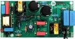
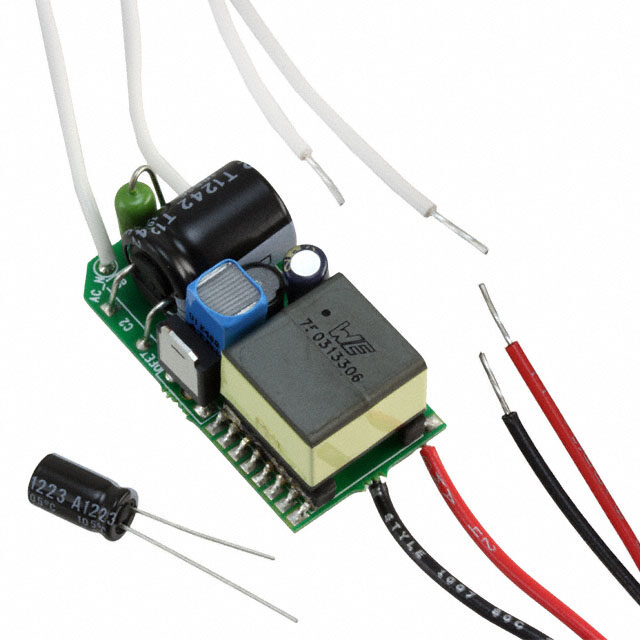
| 描述 | BOARD EVAL NCL30051 LED DRIVER电源管理IC开发工具 90-265VAC 60W ISO CC EVB |
| 产品分类 | |
| 品牌 | ON Semiconductor |
| 产品手册 | |
| 产品图片 |
|
| rohs | 符合RoHS无铅 / 符合限制有害物质指令(RoHS)规范要求 |
| 产品系列 | 电源管理IC开发工具,ON Semiconductor NCL30051LEDGEVB- |
| 数据手册 | |
| 产品型号 | NCL30051LEDGEVB |
| 产品 | Evaluation Boards |
| 产品种类 | 电源管理IC开发工具 |
| 使用的IC/零件 | NCL30051 |
| 其它名称 | NCL30051LEDGEVB-ND |
| 商标 | ON Semiconductor |
| 工具用于评估 | NCL30051 |
| 所含物品 | 板 |
| 标准包装 | 1 |
| 特性 | 可调光 |
| 电压-输入 | 90 ~ 265 VAC |
| 电压-输出 | 35 V ~ 50 V |
| 电流-输出/通道 | 1A |
| 类型 | Power Factor Correction |
| 设计资源 | 点击此处下载产品Datasheet点击此处下载产品Datasheethttp://www.onsemi.com/pub/Collateral/NCL30051LEDGEVB_GERBER.ZIP点击此处下载产品Datasheet |
| 输入电压 | 90 VAC to 265 VAC |
| 输出和类型 | 1,隔离 |
| 输出电压 | 35 V to 50 V |
| 输出电流 | 1.5 A |


- 商务部:美国ITC正式对集成电路等产品启动337调查
- 曝三星4nm工艺存在良率问题 高通将骁龙8 Gen1或转产台积电
- 太阳诱电将投资9.5亿元在常州建新厂生产MLCC 预计2023年完工
- 英特尔发布欧洲新工厂建设计划 深化IDM 2.0 战略
- 台积电先进制程称霸业界 有大客户加持明年业绩稳了
- 达到5530亿美元!SIA预计今年全球半导体销售额将创下新高
- 英特尔拟将自动驾驶子公司Mobileye上市 估值或超500亿美元
- 三星加码芯片和SET,合并消费电子和移动部门,撤换高东真等 CEO
- 三星电子宣布重大人事变动 还合并消费电子和移动部门
- 海关总署:前11个月进口集成电路产品价值2.52万亿元 增长14.8%


PDF Datasheet 数据手册内容提取
NCL30051LEDGEVB 35-50 Volt, Up to 1.5 Amp, Offline Power Factor Corrected LED Driver with Flexible Dimming Options Evaluation Board User's http://onsemi.com Manual EVAL BOARD USER’S MANUAL Introduction This application note describes a 60 W, off−line, power these applications have accessibility issues that would factor corrected, line isolated, LED driver using significantly reduce maintenance costs given the LEDs long ON Semiconductor’s new NCL30051 two−stage controller. operating lifetime. This specific driver design is tailored to This controller contains the control circuitry for both a support LEDs such as the Cree XLAMP(cid:2) XP−G and ® critical conduction mode (CRM) boost power factor XM−L, and OSRAM Golden DRAGON Plus that have corrector (PFC), and a fixed frequency, series resonant maximum drive currents of at least 1000 mA. These LEDs half−bridge converter, and is housed in a 16 pin SOIC exhibit good efficacies at higher drive currents allowing package. The high level of integration and low pin count is fewer LEDs to be used to achieve the same light output. For based on a novel control topology where the PFC output example, the Cree XLAMP XM−L is rated for up to 3 A bulk voltage is adjusted via closed loop to change the drive current and has a very low typical forward voltage of amount of power transferred by the fixed duty cycle 3.1 V @ 1500 mA drive current. At 1500 mA and 85°C half−bridge. The resonant half−bridge essentially functions junction temperature, in cool white, each LED generates as a dc−to−dc step−down transformer. This approach is from 440−475 lumens typical with an efficacy of greater simpler to implement and stabilize compared to the more than 100 lm/W. So with just 12 LEDs, the source lumen complex LCC topology where the frequency of the resonant output would be in the range of 5200−5700 lumens at 85°C controller is varied to change the amount of power junction temperature and the typical load power would be transferred to the load. The fixed frequency and symmetrical ~53 W which is over 100lm/W. duty cycle of the resonant half−bridge clocking allows for This application note also focuses on various options for very simple transformer design. This topology is capable of dimming including PWM, analog and bi−level dimming. powering series LED loads with efficiencies reaching 90%. Intelligent dimming takes full advantage of the instant This is mainly due to the CRM power factor corrector and turn−on characteristics of LEDs and combines it with the very high efficiency of the resonant half−bridge which lighting controls to save significant energy without results in zero current and voltage switching in the power compromising lighting quality or user safety and comfort. MOSFETs. Such efficiencies would be quite difficult using Some traditional large area light sources are difficult to a conventional flyback converter in the second stage. easily dim and have long turn−on times to full brightness. Constant voltage, constant current control (CVCC) is This is not the case with LEDs as they can quickly be turned handled on the secondary side of the power circuit using on and off and their lifetime improves when dimmed ON Semiconductor’s NCS1002 CVCC controller with because the average operating junction temperature is integrated reference. Although this particular design reduced. PWM and analog dimming are traditional represents a 60 W nominal application, the controller techniques for dimming. Bi−level or multi−level dimming topology is ideal for power levels to 200 W and higher. This uses these techniques and adds sensors or controls (motion, specific design is available as evaluation board networked, or timer based) to incorporate two or more NCL30051LEDGEVB. discrete lighting levels. This allows additional energy There are a wide variety of medium power lighting savings without compromising safety and convenience. applications that would benefit from replacing the This is especially useful in outdoor and underground traditional light source with an LED source including street lighting were bi−level control can reduce the light level lights, refrigerator cases, parking garages, wall washers, based on time−of−day or activity detection to save power wall packs and architectural lighting. All of these without compromising safety. In fact the California Lighting applications have high operating hours, challenging Technology recently published a study where bi−level LED environmental conditions, and can benefit from advanced lighting saved 87% over conventional 70 W HID outdoor dimming control to further save energy. Moreover many of pathway bollards. © Semiconductor Components Industries, LLC, 2011 1 Publication Order Number: November, 2011 − Rev. 1 EVBUM2039/D
NCL30051LEDGEVB Beyond the power stage design, circuitry is provided for PWM dimming frequency 160 Hz – demonstrating three types of dimming control: 300 Hz with external signal input • Analog dimming with a 0 to 10 V programming signal; (referenced to a secondary side signal • ground) Bi−level dimming with a simple logic level input Dimming range > 10:1 signal; • 0−10 V (100K) analog voltage input PWM dimming using an onboard oscillator with dimming, 1 = minimum, 10 V is 100% variable pulse width. on (range dependent on nominal AC These three dimming functions are incorporated on an input) optional plug−in DIM card. Without the card, the demo Protection: Short Circuit Protection board can be dimmed with a user provided PWM input Open Circuit Protection < 60 V peak signal operating from 150 to 300 Hz. The maximum output Over Temperature – (optional) voltage can be adjusted via selection of a single resistor; Over Current Protection − Auto however, it is compliant enough to handle almost a 2:1 recovery output voltage compliance range depending on the string Over voltage protection (input and forward voltage and worst case high line voltage. The optional output) default output current is set at 1 A, but a maximum DC output current of 1.5 A is available by modifying a single Primary Side Circuitry resistor value. Higher currents can be supported with The primary side circuit schematic is shown in Figure 1. different transformer designs. The power level of this design It contains the PFC and resonant half−bridge along with the is targeted at applications operation below 60 Vdc associated bias, drive, and primary feedback circuitry. As maximum and below 100 VA to be under the maximum shown in the primary side schematic, the circuit grounds power requirements of IEC (EN) 60950−1 (UL1310 should are segregated into three areas (logic, drive, and Class 2) supplies. The specification table below lists the key power) and interconnected at strategic “star” or “tree” points design objectives. as shown to minimize ground loops and cross talk interaction. For optimum circuit performance and stability, Specifications it is critical that “star” grounding be used for the PCB layout. Universal Input: 90 − 265 Vac (up to 305 Vac with Logic level timing and filter components such as C10, C12, component changes) C14, C15, C17, and C16 should be located as close to main Frequency 47 − 63 Hz controller U1 as possible. Power Factor: > 0.9 (50−100% of Load with Jumper JMP1 and test point terminals are provided to dimming) facilitate testing the PFC and resonant half−bridge Harmonic Content EN61000−3−2 Class C Compliance separately. Jumper JMP3 can be used as a wire loop for a Efficiency > 88% at 50 −100% of 50 W, Iout = 1 A clip−on current probe to check the current waveform profile / Vf = 50 V and tuning of the resonant half−bridge. Target UL1310 Class 2 Dry/Damp, isolated < Referring to Figure 1, a combination common and 100 VA and < 60 V peak differential mode conducted EMI filter is incorporated at the Vmax Range: 35 to 50 Vdc (selectable by resistor mains input. The leakage inductance of L1 in conjunction divider) with “X” capacitors C1 and C2 form a differential mode Constant Current filter. Common mode filtering is achieved via the coupled Iout Range: 0.7 − 1.5 A, 1 A nominal (selectable by inductance of L1 and “Y2” capacitor C27 which ac couples resistor) the primary and secondary grounds. In this particular design, Vout Compliance >50 to 100% of Vout the simple common mode filter indictor of L1 was sufficient Current Tolerance ±2% or better to pass EN55022, Level A for commercial applications. A Cold Startup < 1 sec typical to 50% of load plot of the conducted EMI is shown in Figure 14 and the Pout Maximum: 60 W harmonic line current profile is shown in Figure 15. Dimming: Two Step Bi−level Analog Dimming PWM dimming with optional DIM board http://onsemi.com 2
NCL30051LEDGEVB InAC associated U1 pins as possible.7. C10, C17, and Q7/R40 should be as close to6. Q1 requires small heatsink.5. L2 and T1 are PQ2020 cores with 14 pin bobbins. ground planes as shown in schematic. should be single−point connected to the power and d4. NCL30051 signal grounds and associated componen is signal/logic ground, green is drive ground. ground plane areas − blue is power ground; black3. Heavy schematic lines are recommended2. L1 is Coilcraft E3492−AL (2.9 mH)1. Q2A, Q2B are D−Pak devices. NOTES: TH1 T400V0.22uR1B”X””X”0.220.22C3x 2560KC1C2x 4R1AL1MRA4007D1 − D4 1.5AF1 rivts F 0.5W680KR12 0.5W680KR11 e OR 1 pen13 820pF C100.1 C11 4.7K, 0.5W R10 27.4kR9 5.6nF0.25W10R7C8 1.2KR8 10KR17 TO−220Q146 3700uHL2 1N5406D5 100pF C12 27.4kR19 2.7M,0.5WR18 MRA4007 D12 2.7M,0.5WR14 MMZ1ASZ5248B 0.5W0.15R2C C MURS36D6 L 5 4 0 ogic/signal Ground 1nF0.11KR16C14C150.68uFC13 89 710 611 125 134 143 152 161 NCL30051U11.2K R40 MURA160 D10 MD9Z1B Drive G0.5W560KR4400V82 uF 400V82 uF0.5W560KR3 JMP1 HVout 35V330uF C16 D11 RA4007 round HVin 1.2nFC17 Q3 A06LTGMMBTQ8 25V0.22 C9 R6 R NDD0 4148BMMSDD13 2907AMMBT Q710AR43M GNDM 10K NDD Q2B 10K 5 Q2A4N60ZTM PS2561A 32 41U3 2.7KR15 5.1KR42 PS2561A3206LTGPWMBT14U2 10KR41 PlaneGroundPirmary URA160400VD80.1uF C7 04N60ZT 5 JMP32 400VC6D70.1uFURA160 C FeedbaCVCC A C M Dim A C27 14 11 10 7 T1 c k Figure 1. Primary Side Schematic http://onsemi.com 3
NCL30051LEDGEVB Power Factor Correction Section Resonant Half−Bridge Section The boost power factor corrector circuit is composed of The resonant half−bridge is comprised of MOSFET MOSFET Q1, boost diode D6, boost inductor L2, and the switches Q2A and Q2B, resonant capacitors C6/C7, components associated with the PFC control section and transformer T1, and the associated components and pins of the NCL30051 control IC U1. D5 provides a bypass half−bridge driver section of U1. Since Q2A, the upper diode to prevent resonant (L/C) charging of series boost MOSFET is “floating” at a switched node, a “bootstrap” output capacitors C4 and C5 during initial startup when the driver bias supply composed of D11, C9 and the internal line voltage is first applied. Two 400 Vdc capacitors are used circuitry of U1 is implemented for gate drive of this in series for the bulk capacitors to accommodate the 550 MOSFET. maximum bulk voltage. 300 Vdc rated capacitors could have The half−bridge is operated with a fixed frequency, also been used in this application. C3 is a polypropylene film symmetric duty ratio (with dead time between each capacitor used to “stiffen” the input source impedance to the half−cycle) signal and is powered from the PFC bulk boost converter and provide EMI filtering. voltage. The NCL30051 controller is rated for up to 600 Vdc Operating bias (V ) for the control IC U1 is derived from operation in the half−bridge section, so factoring in system CC the low voltage auxiliary winding on boost choke L2. This derating, a maximum operating PFC bulk voltage in the is essentially a charge pump circuit comprised of R7, C8, Z1, 480−510 V range is recommended. Resonant circuit D10 and V filter capacitors C15 and C16. operation is achieved by resonating the leakage inductance CC The power factor correction circuit operates in critical (or of T1’s primary with capacitors C6/C7 which appear in boundary) conduction mode (CRM) and, hence, has a parallel. By adjusting the L/C ratio of these parameters to variable switching frequency depending on line and load match the switching frequency of the gate drive output of conditions. Since the L2 inductor current always drops to U1, resonant operation is possible with very low switching zero before Q1 is turned back on again, boost diode D6 will losses in MOSFETs Q2A and Q2B. The frequency of the have essentially no reverse recovery losses when Q1 is half−bridge drive is set by the C capacitor C10. This value t switched on each cycle. In addition the turn−on gate drive can be changed to accommodate the resonant frequency requirement for Q1 is minimized since the MOSFET current determined by C6/C7 and T1’s leakage inductance. Without always starts at zero, however, complementary driver any complex winding structure, the leakage inductance of Q3/Q8 is implemented in the gate drive line for efficient T1 came out to about 100 (cid:2)H with the transformer design switching of Q1. shown in Figure 4. The waveform of the sinusoidal primary In some cases it is possible to vary the resistance of current (45 W output) is shown in Figure 2. The use of fixed R11/R12 slightly to improve the power factor at high line. frequency, resonant switching in the half−bridge creates a This circuit provides “feed forward” signal information to condition of zero current switching in the MOSFETs which the PFC on−time setting capacitor C17. It should also be results in very high conversion efficiency. Diodes D7 and noted that resistor R9 is used to provide the zero current D8 provide voltage clamping to the bulk rail in the event of detect signal (or de−magnetizing signal) to the chip from parasitically generated voltages or transients during start up L2’s aux winding so that the circuit can operate in true CRM. and/or dynamic operation. Figure 2. Resonant Half−Bridge Current Waveform http://onsemi.com 4
NCL30051LEDGEVB Secondary Side Circuitry Output voltage sensing is achieved via the sense divider The secondary winding of the half−bridge transformer, of R28 and R29 and U4A. The maximum output voltage can the full−wave, center−tap rectifier, and the associated be adjusted by the value of R28 and is set to approximately secondary side circuitry are shown in the schematic of 50 V in this application. Figure 3. The secondary rectifier D16 is a dual Schottky Both amplifiers drive optocoupler U3 which controls the device and, because of the symmetrical duty ratio, only a pulse width of the PFC MOSFET by pulling compensation modest amount of capacitive filtering is necessary to pin 8 low on the main controller U1. In this way the bulk attenuate the high frequency output ripple. In this design a output voltage of the PFC is regulated so as to provide a paralleled pair of 4.7 (cid:2)F, 100 Vdc film capacitors were used. correct high voltage dc input to the resonant half−bridge The current and voltage sensing circuitry is based around converter. The amplifier whose output is lowest will be the NCS1002 CVCC controller. The specific sensing dominant, thus providing constant current, constant voltage circuitry is essentially identical to that used in control with a smooth transition at the CVCC knee. To ON Semiconductor application note AND8470 for the minimize the Miller capacitance effects of optocoupler U3’s NCL30001 LED controller and will only be briefly photo transistor to the feedback loop, R15 and D13 have described here. been added to force extra current through the opto transistor Current regulation is accomplished by section B of U4. without loading pin 8 of U1. The output current is sensed by resistor R22 and the dc Since the PFC also senses the bulk output voltage via output current level can be adjusted by changing R26. If resistor network R14, R18, and R19, this divider is set via PWM dimming is used, the circuit of Q5, C22, R31 and R32 R19 such that this “inner” voltage loop is closed when the form a sample and hold circuit that prevents the current pulse bulk voltage reaches 550 Vdc so as to not prematurely interruptions through current sense resistor R22 from interfere with the secondary voltage loop of U4A. Note that corrupting the dc current sense information presented to if the secondary voltage feedback loop were to fail, the inner pin 6 of U4B. This keeps the peak current output level PFC voltage feedback loop would clamp the bulk voltage to constant during PWM dimming. approximately 550 Vdc. http://onsemi.com 5
NCL30051LEDGEVB 2. Heavy sche1. D16 require Notes: C PWM Dim A Ground PlaneTo Primary Sid MMSD4148 D15 C FeedbackCVCC A C18,19,20 XfmrT1 matic lines are recos small heatsink. 2.7K R39 2.2nF C27 e MMBT2907A Q90.1 C26 MMSZ5245BZ2MMSD4148 D14 2.2K R20 14 11 10 7 MBRF10H150D16 mm 47 R2 e K 3 n V ded ground plane areas. to U3internal 34+VrefU4A1−247KR24 NCS10021uF 5C28+IsU4B7−68 0.22uF C25 cc = 14V15K Q4RMJD243G C19C18 100 V x 24.7 uF 0.11 C30C 2.5V 68KR26 1nF C24 2.7KR25 Is , 0.5W 21 100V0.1uF C20 0nF 29 6.2KR27 3.9KR29 78.7KR28 Vs C G 23 0.50.1 R2 nd 0.1 W0 2 N C L30051 LED D 2212LMMUN Q1010 R3510 R34 10 VccR33 2N7002KT1G2.7K R32Q5 1001uFR31 C225.1K R30 Sample & HoldCurrent Sense 100V0.1uF C21 r iv e r C Q VCC Secondary S P1 1 2 3 JMP2 Card not usedJumper if DIM 5 610KR3710KR3810 R36MMBTA06LT1G e K 6 n s in g Common Dim outAnalog Vref In Vcc In Out PWM G nd J3 − LED J2 LED + CardOptionsControlDimming 100−200HPWM In Cathode Anode z Figure 3. Secondary Side Schematic http://onsemi.com 6
NCL30051LEDGEVB Resonant Half−Bridge Transformer Design (T1) actually purposely designed in, however, with the three layer Since the half−bridge transformer operates in a fixed primary and adequate insulating tape between the primary frequency, symmetrical duty ratio, the design becomes very and secondary there should be adequate leakage inductance straightforward. A half−bridge converter switches 1/2 of that will facilitate a resonant capacitor with a common value bulk voltage across the transformer primary due to the that will obtain a reasonable resonant frequency that can be capacitive divider network formed by resonant capacitors accommodated by the internal half−bridge clock in the C6 and C7. By choosing the maximum bulk voltage at about NCL30051 controller. By shorting the transformer 500 Vdc and assuming a maximum output voltage of 50 V, secondary pins out with very short wires, the primary the turns ratio on the transformer will be: leakage can be measured with an inductance meter. In this V /2 divided by 50 V = 250/50 = 5 design the leakage inductance worked out to be between 90 bulk out So, a turns’ ratio of 5:1 is required between the primary and 100 (cid:2)H, sufficient to produce a resonant frequency of and one of the half’s of the−secondary(note: push−pull 36 kHz with a pair of 0.1 (cid:2)F capacitors (in parallel output rectification!). All that is required now is to effectively) for C6 and C7. It turned out that a clock timing determine the minimum number of primary turns necessary capacitor of 1 nF for C10 sets the switching frequency to to avoid core saturation and then ratio the secondary turns about 36 kHz which provided the optimum tuning as from this point. The selected core is a PQ−2020 with a cross displayed in primary current waveform of Figure 2. The sectional core area (Ae) of 0.6 cm2. Using the transformer design summary of the transformer T1 is shown in Figure 4. design relationship: Since the output current and/or voltage is regulated by controlling the PFC bulk voltage, the value of the bulk V(cid:3)D(cid:3)108 20V(cid:3)1(cid:3)108 Np(cid:2) (cid:2) voltage will be directly proportional to Vout via the turns 4(cid:3)F(cid:3)BM(cid:3)Ae 4(cid:3)35kHz3200G(cid:3)0.6cm2 ratio of the transformer. For example, if we have an LED (cid:2)96.7turns string with a nominal forward voltage of 40 V, the bulk voltage will be regulated at: V x Np/Ns x 2 = 40 x 5 x 2 Where: Np is the minimum primary turns out = 400 Vdc (where two represents the fact that the needed half−bridge primary switches only 1/2 of the bulk voltage). V is the max voltage across the Herein highlights a limitation of this topology in cases primary (with a little margin) where the string voltage may be very low. For a V of 32 V, F is the switching frequency f the bulk voltage will be 320 Vdc and this puts a limit on the Bm is the maximum flux density in the maximum line voltage in which the PFC boost converter can ferrite core function. The bulk voltage must always be higher than the Ae is the cross sectional area of the peak of the line voltage for the boost converter to work, so core at 230 Vac input, the line peak is 1.4 x 230 = 322 V so now The average primary current will be a little more than we have reached the lower limit of the LED forward voltage 60 W / 250 Vdc x 0.95 = 228 mA assuming close to 95% range. Obviously at 120 Vac (V = 170 Vdc) we could converter efficiency. The rms value will actually be a little peak feasibly allow the output V to go even as low as 25 Vdc higher but AWG # 28 magnet wire will easily handle this and f without any problems (25 Vdc x 5 x 2 = 250 Vdc bulk which 96 turns can comfortably be wound over 3 layers with 32 is still higher than Vac peak). Careful analysis of the turns per layer. throughput voltage conversion and proper selection of the The number of secondary turns will be 96 / 5 = 19.2 turns transformer turns ratio will allow optimization for a given so 19 turns will be close enough. It turns out that due to the LED application. A maximum operating PFC bulk voltage center tapped secondary, two strands of #26 magnet wire of 510 Vdc is recommended for adequate safety margins. wound bifilar on top of the primary will make the secondary Examples and further discussions of the circuit limitations easily handle up to 1.5 A output current. The primary are addressed below under “Topology Limitations”. leakage inductance is the only unknown factor that was not http://onsemi.com 7
NCL30051LEDGEVB Part Description: Resonant Half−bridge Transformer − 60 W, 35 kHz (Rev 3) Schematic ID: T1 Core Type: PQ20/20, Ferroxcube 3C95 or equivalent material Primary Inductance: 6 mH minimum Leakage Inductance: 90 − 100 uH nominal (resonant half−bridge, leakage inductance is Lr) Bobbin Type: PQ20/20 14 pin PC mount bobbin Windings (in order): Winding # / type Turns / Material / Gauge / Insulation Data Primary winding (2 − 5) 96 turns of #28 HN magnet wire over 3 layers, 32 turns per layer approx. Self−leads to pins. Insulate with Mylar tape sufficient for 3 kV Hipot to next winding. Secondary winding (7,11 − 10,14) 19 turns of 2 X #26 magnet wire bifilar wound over two layers. Self−leads to pins per schematic below. Final insulate with Mylar tape. Note: The critical parameter is to achieve a leakage inductance of 90 − 100 uH with a min primary inductance of 6 mH. The overall turns can be increased or decreased to achieve this as long as the turns ratio remains 5:1. Vacuum varnish assembly. Hipot: 3000 volts from Primary to Secondary (1 minute) Schematic Lead Breakout / Pinout Bottom View 14 1 2 7 2 11 11 3 Primary Secondary 14 10 4 5 10 5 7 6 Figure 4. Resonant Half−Bridge Transformer Design (T1) http://onsemi.com 8
NCL30051LEDGEVB PFUCs iCnhgo kteh De esPigFnC ( L2d)esign approach illustrated in L(cid:2)N(cid:3)Bmax(cid:3)Ae and Lg(cid:2)0.4(cid:3)(cid:3)N(cid:3)Ipk Ipk(cid:3)108 Bmax ON Semiconductor Application Note AND8123, we can analyze the PFC choke design. Where: N is the number of turns B is the max flux density Inductor rms current at 50 W output and 85 Vac input: max Ipk is the peak inductor current 0.72 A Ae is the core cross sectional area (cm2) Inductor peak current at 50 W out and 85 Vac input: 1.75 A Lg is the total core gap (cm) Maximum inductance for reasonable switching frequency: Substituting the known values into first equation for N = 1200 (cid:2)H max. 75 turns, B = 3000 gauss, Ae = 0.6, and Ipk = 1.75 A we max Turns ratio to aux winding to produce a 15 to 18 Vdc VCC: get L = 770 (cid:2)H which is less than the max of 1200 (cid:2)H. This 9:1 or 10:1 will result in a switching frequency of 70 kHz min and To maintain component consistency, a PQ−2020 ferrite 200 kHz max for typical operation, so this is probably a core was also selected for the PFC choke. Based on an rms reasonable inductance to start with. We could increase the choke current of 0.72 A and an average switching frequency inductance and lower the PFC switching frequency by of around 100 kHz, three strands of AWG #30 magnet wire adding more turns, but this would probably require a larger was chosen for the main winding to minimize ac losses. core. Calculations based on the approximate wire diameter (2 x In order to prevent saturation, the core must be gapped per 0.012” or 0.61 mm), and a core bobbin inside winding width the second equation. Substituting in the known parameters of about 0.47” (12 mm); it appears that 75 turns of this wire we get Lg = 0.055 cm or 0.022 inches. Since this is the total can comfortably be wound on 4 or 5 layers with about 18 gap, we would use half of this length if we were gapping all turns per layer. Using the above parameters from the design three pole legs of the core. This gap should also give us the spreadsheet, and the following inductor relationships we can required inductance of about 700 (cid:2)H. The final choke determine the optimum design using this PQ−2020 core: design is shown in Figure 5. http://onsemi.com 9
NCL30051LEDGEVB Part Description: PFC Choke − 60 W, 100 kHz (CRM); Rev. 4 (6/8/10) Schematic ID: L2 Core Type: PQ20/20, Ferroxcube 3C95 or equivalent material Core Gap: Gap for 675 uH +/−25 uH across pins 1 to 3. Inductance: 650 − 700 uH nominal Bobbin Type: PQ20/20 14 pin PC mount bobbin Windings (in order): Winding # / type Turns / Material / Gauge / Insulation Data Main winding (1 − 3) 75 turns of 3 strands of #30 trifilar wound. Wire can be twisted if desired. Self−leads to pins. Insulate with 2 or 3 layers of Mylar tape to next winding. (Other option: 2 strands #28 bifilar) Vcc winding (4 − 6) 8 turns of #30 magnet wire spiral wound over one layer. Self−leads to pins. Final insulate with Mylar tape. Vacuum varnish assembly. Hipot: 1000 volts from main winding to Vcc winding.. Schematic Lead Breakout / Pinout Bottom View 1 14 1 2 Main − 75T 11 3 of 3 x #30 3 10 4 4 5 Vcc − 8T 7 6 of #30 6 Figure 5. PFC Choke Design Details (L2) http://onsemi.com 10
NCL30051LEDGEVB Dimming Capabilities not installed. More details of the DIM card operation can be To demonstrate the LED dimming capabilities of this found in AND8470. A table for configuring the three circuit, the same DIM control card used in the NCL30001 different operating modes is shown below and the schematic LED driver circuit described in AND8470 has been used for the DIM card circuit is shown in Figure 7. here. Dimming can be accomplished using three methods: pulse width modulation (PWM) of the output current; Modifications; Jumper analog current dimming where the current reference voltage Dimming Configuration Configurations for U4B is modified via a 1 to 10 V control signal to linearly External PWM dimming Omit DIM card; short pins 2 and control the output current to the LEDs; and bi−level input 3 of P1. dimming in which a logic level signal will lower the LED Inject PWM signal into J3 intensity level by reducing the LED output current. Without Internal PWM dimming Add DIM card with JMP1 added this DIM card, a PWM input terminal (J3) is still provided to P1 on DIM card; Add JMP3 to for an external 160 to 300 Hz PWM input signal to control P2 on DIM card. Adjust pot R1 to vary pulse width. the output current. This is done by switching transistor Q6 on and off which in turn switches the sample and hold Bi−Level Dimming Add DIM card with JMP1 (P1) removed; Add JMP3 to P2 on transistor gate drive, and toggles optocoupler U2 which card; Connect switch from TP1 switches U1’s Ct pin (2) via buffer transistor Q7. This pin, and TP2. Closed switch gives when grounded, will terminate drive to the half−bridge low dim level. MOSFETs (Q2A, Q2B) thus rapidly stopping output current Analog Dimming, Internal Add DIM card with JMP1 (P1) flow. Due to the low value of output capacitors C18 and C19, Adjust removed: Add JMP2 to P2; Adjust pot R9 for LED a rectangular wave signal in the frequency range of 160 to brightness. 300 Hz will adequately PWM the output current with good Analog Dimming, External Add DIM card with JMP1 (P1) rise and fall times (see Figure 6). C1 on the DIM card sets Adjust removed. Add JMP2 to P2. this frequency. Higher dimming frequencies can but used Remove pot R9 and wire in but the dynamic range of the dimming can be limited due to external 100k potentiometer to TPs 2, 3 and 4. TP3 is the pot waveform fall times. It should be noted that jumper J2 across wiper. Adjust external pot for pins 2 and 3 of connector P1 is necessary if the DIM card is LED brightness. Figure 6. PWM Dimming Mode – Output Current Profile Depending on the selected PWM dimming frequency (C1 modulation at some pulse widths. It is best to select the of Figure 7), it is possible to get a slight beat between this PWM dimming frequency to be in between the line frequency and a harmonic of the line frequency. Depending frequency harmonics. Thus, 160 or 220 Hz would be on the magnitude of the overall output ripple and the recommended optimum PWM frequencies for a line selection of C4 / C5, there is the potential for LED current frequency of 60 Hz. (See section on Output Ripple below.) http://onsemi.com 11
NCL30051LEDGEVB Con1 (to P1) PWM Out 6 JMP1 Dimming Option Control MC1455D Card Schematic (Rev 3) P1 20K R1 U1 Vcc D1 D2 4 8 MMSD 2 3 Notes: 4148 C3 1. Pots R1 and R9 are Vishay/Spectrol 43P Vcc 6 5 0.1 type 20 turn cermet trimmers (Mouser (source) C1 1 part # 594−43P203 and 594−43P104) 2. All caps are SMD ceramic, 25V min. 330nF C2 3. TH1 is PTC thermistor − LS = 5mm 0.1 5 4. All semiconductors are ON Semi parts Vcc In C4 Vcc 1.0 uF 25V R16 2N7002KT1G 10K MMBT2222A Q2 D3 R4 R2 Q1 10K 150K MMSD4148 R3 20K TP1 Bi − Level 3 R5 U2A Switch Vref In + R7 10V (2.5V) C5 4.3K _ TP2 1K 1nF Analog R8 Dimming R9 100K External Dim C6 15K Dim TP3 100K Pot Select R6 Adj P2 5K 10nF Bi−levelJMP3 TP4 or PWM 1 − 10V Temp U2B R11 R10 Analog JMP2 Compensation + 11K R14 10K _ TH1 TBD R12 Analog 30K Vcc Dim Out 2 R15 U2C+ LM324DG 10 _ U2D C9 R13 C8 + 0.1 10K 10nF C7 0.1 _ 1 Common Figure 7. DIM Card Schematic http://onsemi.com 12
NCL30051LEDGEVB Topology Limitations V compliance ratio, however, due to the fact that the f Despite the high efficiency and relatively low complexity primary V is derived from the PFC inductor aux winding, CC of the resonant half−bridge and magnetics design in this experimentation has shown that 20 Vdc is actually the topology, it does have some limitations with respect to the lowest safe minimum V for 120 Vac input for reliable V f CC ac line and output load forward voltage extremes. These maintenance for this design. limitations are primarily due to the fact that, since the 230 Vac: The peak line voltage will be 230 x 1.4 = 322 Vpk. feedback loop controls the output voltage of the power Again, dividing this by 10 yields 32.2 V, or 35 V for the factor corrector, the “bulk” voltage is directly proportional minimum output V with a tolerance margin. f to V or the V of the diode string when operating in the out f 277 Vac: Vpk = 277 x 1.4 = 388 Vdc, so output V minimum normal constant current mode. Since the output (V ) of a f bulk becomes about 40 Vdc. boost converter must always be higher then the peak ac input voltage for the boost converter to function, the relationship 305 Vac: Vpk = 305 x 1.4 = 427 Vdc; so output Vf minimum that V > Vac peak must always be maintained for becomes about 45 Vdc bulk continuous circuit operation and constant output. In the This limitation should considered up front when design example for this demo board, the PFC output bulk designing the LED driver and the consequential effects of voltage is 10 times the output voltage (or Vf) due to the the min and max of the diode string Vf as a result of binning, transformer turns ratio (5:1) and the fact that the resonant forward current and thermal variations. For applications half−bridge switches 1/2 of the bulk across the transformer with high nominal line levels, the transformer turns ratio primary. We can deduce some of the limitations from this becomes more critical when optimizing max and min load fact. The best way is to see the impact the nominal ac line Vf tolerances. As seen from the 120 Vac input example, there voltage has on the output Vf. The NCL30051 has a 600 V is much Vf latitude. max rating on the high side gate driver section (pins 15 and The usable dimming range can also be affected by the 16). As a consequence, assuming an 85% derating, the bulk combination of line voltage and Vf. This is particularly acute bus can be set at 510 Vdc max. Under these conditions V when using the analog dimming mode because this mode out max under no load conditions could be 50 Vdc with the 5:1 also reduces the primary side control circuit VCC as the turns ratio on T1. Assuming this 50 Vdc output max as our output current is reduced. PWM dimming mode has less nominal open circuit Vout, let’s see what the minimum effect on the VCC due to the fact that the VCC capacitor is output Vf can be that will still maintain boost converter peak charged and the reflected peak VCC aux voltage does operation for normal ac line voltages. not appreciably decrease with PWM dimming. Figure 8 shows the limitations of increasing AC input line 120 Vac: In this case the peak line voltage will be 1.4 x 120 on the minimum usable V out. The diagonal section of the Vac = 168 Vpk. Dividing this peak by 10 (T1 turns ratio x f graph indicates converter shutdown and re−start action. half−bridge factor of 2) yields 16.8 V which is less than 1/3 of the V max of 55 V. This would theoretically allow a 3:1 f http://onsemi.com 13
NCL30051LEDGEVB 50 45 40 35 c) d V ( E 30 G A T L O 25 V D R 230 Vac A W 20 R O F D 15 E L 120 Vac 10 5 0 0 100 200 300 400 500 600 700 800 900 1000 OUTPUT CURRENT (mA) Figure 8. Output Current/Voltage Transfer Function versus Line http://onsemi.com 14
NCL30051LEDGEVB 35 30 700 mA 1000 mA c) d V ( E 25 G A T L O V D R A W 20 R O F D E L 15 10 90 115 140 165 190 215 240 265 INPUT LINE VOLTAGE (Vac) Figure 9. Minimum Forward Voltage versus Line and Output Current Efficiency the efficiency is greater than 90% from 35−45 W for both With this topology it is possible to achieve better than 90% 120 and 230 Vac for this 50 W nominal design. efficiency even at modest loads. As illustrated in Figure 10, http://onsemi.com 15
NCL30051LEDGEVB 95 94 93 92 91 %) 230 Vac Y ( C 90 N 120 Vac E CI FI 89 F E 88 87 86 85 34 38 42 46 50 OUTPUT FORWARD VOLTAGE (Vdc) Figure 10. Efficiency versus line and load Power Factor and Input Harmonic Content In addition to power factor, a more critical parameter in The power factor will remain above 0.90 for the rated load some regions is harmonic content. Lighting Power supplies output (1 A) and to minimum Vf levels for 120 Vac input and fall under the IEC61000−3−2 Class C standard and there are down to Vf = 35 Vdc for 230 Vac. As the actual current load vary strict limits on harmonic content for power supplies > is decreased from the rated maximum, the power factor will 25 W. also degrade with lower V. These effects are shown in f Figure 10. http://onsemi.com 16
NCL30051LEDGEVB 1.00 120 Vac 0.95 0.90 0.85 F) P ( R O T 0.80 C A F R 230 Vac E W 0.75 O P 0.70 0.65 0.60 20 25 30 35 40 45 OUTPUT FORWARD VOLTAGE (Vdc) Figure 11. Power Factor versus Forward Voltage (I = 1 A) out 1.00 Iout = 1A 0.95 F) 0.90 P Iout = 0.5A ( R O Iout = 0.7A T C 0.85 A F R E W O 0.80 P 0.75 0.70 90 115 140 165 190 215 240 265 INPUT LINE VOLTAGE (Vac) Figure 12. Power Factor versus Output Current http://onsemi.com 17
NCL30051LEDGEVB 30 25 %) al ( et m a 20 d n u F of e g a nt 15 e c er P nt e urr Limit (%) C 10 c Measured (%) ni o m ar H 5 0 2 3 5 7 9 11 13 15 17 19 21 23 25 27 29 31 33 35 37 39 Harmonic Figure 13. Harmonic Levels (230 Vac input, Full Load) Dimming Effects on Power Factor and V Limits f The power factor is also affected by both analog and PWM dimming and is reduced at lower dimming levels. This is shown in Figure 14. http://onsemi.com 18
NCL30051LEDGEVB 1.00 120 Vac; Analog Dim 0.95 120 Vac; PWM Dim 0.90 230 Vac; Analog Dim F) P ( R O 230 Vac; PWM Dim T C 0.85 A F R E W O 0.80 P 0.75 0.70 0 10 20 30 40 50 60 70 80 90 100 PERCENT OF FULL LOAD (%) Figure 14. Power Factor versus Dimming Dimming Limitations the bulk will be reflected to the output by the product of the PWM dimming is effective down to less than 5% duty transformer turns ratio and the half−bridge switch voltage ratio for 120 and 230 Vac within the Vf ranges shown in the reduction ratio, or, as mentioned previously, 5 x 2 = 10. Since graphs of Figure 8 above. It is not recommended to take the power factor control loop must have a low bandwidth to PWM dimming to zero as this will ultimately result in the produce high power factor, the 120 Hz bulk ripple will power supply going into a start−stop “hiccup” mode due to naturally be transferred to the output proportionally. In this controller VCC depletion. Analog dimming is limited to 10% example, the use of two bulk capacitors of 82 (cid:2)F in series, (of rated max current) due to depletion of primary circuitry giving a total capacitance of 41 (cid:2)F, was adequate to keep the VCC. output current ripple below 10%. Figure 15 shows the output current ripple with an LED string of V = 40 V. The f Output Ripple magnitude of the ripple is only slightly affected by V and f The output current ripple is primarily a function of the line voltage. amount of bulk capacitance (C4 and C5), and the ripple on http://onsemi.com 19
NCL30051LEDGEVB Figure 15. Output Current Ripple at 1 A Load and V = 40 Vdc f Output Current Profile at Turn−on overshoot. The nature of the start−up profile can be tailored Despite the low control loop bandwidth (approximately by the proper selection of feedback compensation 25 Hz), the output current profile during start−up when the components R23 and C25 around current amplifier U4B. ac line is applied is very well controlled from excessive The start−up profile is shown in Figure 16. Figure 16. Output Current Profile at Supply Turn−on (230 Vac) Line Current and Conducted EMI different line voltages and V points were also captured. f The prototype supplies were tested for FCC Level A These results are shown in the figures below (Green is peak conducted emissions. Waveforms of the input line current at and red is average). http://onsemi.com 20
NCL30051LEDGEVB dBuV NCL30051 − 120 Vac 45 W output 100 90 80 Peak Neutral EN 55022; Class A Conducted, Quasi−Peak 70 EN 55022; Class A Conducted, Average 60 50 40 30 Average Line 20 10 0 1 10 5/18/2010 2:51:02 PM (Start = 0.15, Stop = 30.00) MHz Figure 17. Conducted EMI Spectrum at 1 A with V = 45 V (Red = average) f Figure 18. Input Line Current under Different Operating Conditions http://onsemi.com 21
NCL30051LEDGEVB CONCLUSIONS current needs and illustrates different methods to implement The application note describes the operation of the dimming NCL30051LED Evaluation board and describes the primary design stages including transformer design as well as References operational behaviors. This architecture can achieve very 1.NCL30051 Data Sheet high efficiency for LED lighting applications while meeting 2.NCS1002 CVCC controller data sheet power factor and harmonic content requirements. The 3.ON Semiconductor Application Note AND8470/D evaluation board is flexible to support a range of LED drive 4.ON Semiconductor Application Note AND8427/D 5.ON Semiconductor Design Note DN06068/D Golden DRAGON LED is a registered trademark of OSRAM Opto Semiconductor, Inc. XLamp is a trademark of Cree, Inc. ON Semiconductor and are registered trademarks of Semiconductor Components Industries, LLC (SCILLC). SCILLC reserves the right to make changes without further notice to any products herein. SCILLC makes no warranty, representation or guarantee regarding the suitability of its products for any particular purpose, nor does SCILLC assume any liability arising out of the application or use of any product or circuit, and specifically disclaims any and all liability, including without limitation special, consequential or incidental damages. “Typical” parameters which may be provided in SCILLC data sheets and/or specifications can and do vary in different applications and actual performance may vary over time. All operating parameters, including “Typicals” must be validated for each customer application by customer’s technical experts. SCILLC does not convey any license under its patent rights nor the rights of others. SCILLC products are not designed, intended, or authorized for use as components in systems intended for surgical implant into the body, or other applications intended to support or sustain life, or for any other application in which the failure of the SCILLC product could create a situation where personal injury or death may occur. Should Buyer purchase or use SCILLC products for any such unintended or unauthorized application, Buyer shall indemnify and hold SCILLC and its officers, employees, subsidiaries, affiliates, and distributors harmless against all claims, costs, damages, and expenses, and reasonable attorney fees arising out of, directly or indirectly, any claim of personal injury or death associated with such unintended or unauthorized use, even if such claim alleges that SCILLC was negligent regarding the design or manufacture of the part. SCILLC is an Equal Opportunity/Affirmative Action Employer. This literature is subject to all applicable copyright laws and is not for resale in any manner. PUBLICATION ORDERING INFORMATION LITERATURE FULFILLMENT: N. American Technical Support: 800−282−9855 Toll Free ON Semiconductor Website: www.onsemi.com Literature Distribution Center for ON Semiconductor USA/Canada P.O. Box 5163, Denver, Colorado 80217 USA Europe, Middle East and Africa Technical Support: Order Literature: http://www.onsemi.com/orderlit Phone: 303−675−2175 or 800−344−3860 Toll Free USA/Canada Phone: 421 33 790 2910 Fax: 303−675−2176 or 800−344−3867 Toll Free USA/Canada Japan Customer Focus Center For additional information, please contact your local Email: orderlit@onsemi.com Phone: 81−3−5817−1050 Sales Representative http://onsemi.com EVBUM2039/D 22
Mouser Electronics Authorized Distributor Click to View Pricing, Inventory, Delivery & Lifecycle Information: O N Semiconductor: NCL30051LEDGEVB