ICGOO在线商城 > 集成电路(IC) > 逻辑 - 缓冲器,驱动器,接收器,收发器 > NC7SP125L6X
 Datasheet下载
- 型号: NC7SP125L6X
- 制造商: Fairchild Semiconductor
- 库位|库存: xxxx|xxxx
- 要求:
| 数量阶梯 | 香港交货 | 国内含税 |
| +xxxx | $xxxx | ¥xxxx |
查看当月历史价格
查看今年历史价格
NC7SP125L6X产品简介:
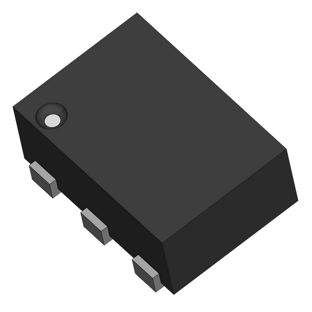
ICGOO电子元器件商城为您提供NC7SP125L6X由Fairchild Semiconductor设计生产,在icgoo商城现货销售,并且可以通过原厂、代理商等渠道进行代购。 NC7SP125L6X价格参考。Fairchild SemiconductorNC7SP125L6X封装/规格:逻辑 - 缓冲器,驱动器,接收器,收发器, Buffer, Non-Inverting 1 Element 1 Bit per Element 3-State Output 6-MicroPak。您可以下载NC7SP125L6X参考资料、Datasheet数据手册功能说明书,资料中有NC7SP125L6X 详细功能的应用电路图电压和使用方法及教程。
| 参数 | 数值 |
| 产品目录 | 集成电路 (IC)半导体 |
| 描述 | IC BUFFER TRI-ST ULP 6MICROPAK缓冲器和线路驱动器 Bufer 3-STATE Output |
| 产品分类 | |
| 品牌 | Fairchild Semiconductor |
| 产品手册 | |
| 产品图片 |
|
| rohs | 符合RoHS无铅 / 符合限制有害物质指令(RoHS)规范要求 |
| 产品系列 | 逻辑集成电路,缓冲器和线路驱动器,Fairchild Semiconductor NC7SP125L6X7SP |
| 数据手册 | |
| 产品型号 | NC7SP125L6X |
| PCN设计/规格 | |
| 产品种类 | 缓冲器和线路驱动器 |
| 传播延迟时间 | 23.4 ns at 1.2 V |
| 低电平输出电流 | 2.6 mA |
| 供应商器件封装 | 6-MicroPak |
| 元件数 | 1 |
| 其它名称 | NC7SP125L6X-ND |
| 包装 | 带卷 (TR) |
| 单位重量 | 18 mg |
| 商标 | Fairchild Semiconductor |
| 安装类型 | 表面贴装 |
| 安装风格 | SMD/SMT |
| 封装 | Reel |
| 封装/外壳 | 6-UFDFN |
| 封装/箱体 | MicroPak-8 |
| 工作温度 | -40°C ~ 85°C |
| 工厂包装数量 | 5000 |
| 最大工作温度 | + 85 C |
| 最小工作温度 | - 40 C |
| 极性 | Non-Inverting |
| 标准包装 | 5,000 |
| 每元件位数 | 1 |
| 每芯片的通道数量 | 1 |
| 电压-电源 | 0.9 V ~ 3.6 V |
| 电流-输出高,低 | 2.6mA,2.6mA |
| 电源电压-最大 | 3.6 V |
| 电源电压-最小 | 0.9 V |
| 系列 | NC7SP125 |
| 输入线路数量 | 1 |
| 输出类型 | 3-State |
| 输出线路数量 | 1 |
| 逻辑类型 | CMOS |
| 逻辑系列 | TinyLogic ULP |
| 高电平输出电流 | - 2.6 mA |


- 商务部:美国ITC正式对集成电路等产品启动337调查
- 曝三星4nm工艺存在良率问题 高通将骁龙8 Gen1或转产台积电
- 太阳诱电将投资9.5亿元在常州建新厂生产MLCC 预计2023年完工
- 英特尔发布欧洲新工厂建设计划 深化IDM 2.0 战略
- 台积电先进制程称霸业界 有大客户加持明年业绩稳了
- 达到5530亿美元!SIA预计今年全球半导体销售额将创下新高
- 英特尔拟将自动驾驶子公司Mobileye上市 估值或超500亿美元
- 三星加码芯片和SET,合并消费电子和移动部门,撤换高东真等 CEO
- 三星电子宣布重大人事变动 还合并消费电子和移动部门
- 海关总署:前11个月进口集成电路产品价值2.52万亿元 增长14.8%


PDF Datasheet 数据手册内容提取
Is Now Part of To learn more about ON Semiconductor, please visit our website at www.onsemi.com Please note: As part of the Fairchild Semiconductor integration, some of the Fairchild orderable part numbers will need to change in order to meet ON Semiconductor’s system requirements. Since the ON Semiconductor product management systems do not have the ability to manage part nomenclature that utilizes an underscore (_), the underscore (_) in the Fairchild part numbers will be changed to a dash (-). This document may contain device numbers with an underscore (_). Please check the ON Semiconductor website to verify the updated device numbers. The most current and up-to-date ordering information can be found at www.onsemi.com. Please email any questions regarding the system integration to Fairchild_questions@onsemi.com. ON Semiconductor and the ON Semiconductor logo are trademarks of Semiconductor Components Industries, LLC dba ON Semiconductor or its subsidiaries in the United States and/or other countries. ON Semiconductor owns the rights to a number of patents, trademarks, copyrights, trade secrets, and other intellectual property. A listing of ON Semiconductor’s product/patent coverage may be accessed at www.onsemi.com/site/pdf/Patent-Marking.pdf. ON Semiconductor reserves the right to make changes without further notice to any products herein. ON Semiconductor makes no warranty, representation or guarantee regarding the suitability of its products for any particular purpose, nor does ON Semiconductor assume any liability arising out of the application or use of any product or circuit, and specifically disclaims any and all liability, including without limitation special, consequential or incidental damages. Buyer is responsible for its products and applications using ON Semiconductor products, including compliance with all laws, regulations and safety requirements or standards, regardless of any support or applications information provided by ON Semiconductor. “Typical” parameters which may be provided in ON Semiconductor data sheets and/or specifications can and do vary in different applications and actual performance may vary over time. All operating parameters, including “Typicals” must be validated for each customer application by customer’s technical experts. ON Semiconductor does not convey any license under its patent rights nor the rights of others. ON Semiconductor products are not designed, intended, or authorized for use as a critical component in life support systems or any FDA Class 3 medical devices or medical devices with a same or similar classification in a foreign jurisdiction or any devices intended for implantation in the human body. Should Buyer purchase or use ON Semiconductor products for any such unintended or unauthorized application, Buyer shall indemnify and hold ON Semiconductor and its officers, employees, subsidiaries, affiliates, and distributors harmless against all claims, costs, damages, and expenses, and reasonable attorney fees arising out of, directly or indirectly, any claim of personal injury or death associated with such unintended or unauthorized use, even if such claim alleges that ON Semiconductor was negligent regarding the design or manufacture of the part. ON Semiconductor is an Equal Opportunity/Affirmative Action Employer. This literature is subject to all applicable copyright laws and is not for resale in any manner.
N June 2002 C 7 Revised March 2004 S P 1 2 5 NC7SP125 T TinyLogic ULP Buffer with 3-STATE Output in y L o g General Description Features i c The NC7SP125 is a single Buffer with 3-STATE output from (cid:1) 0.9V to 3.6V VCC supply operation FIdaeiracl hfoildr ’as pUpllitcraa tiLoonws wPhoewree rb a(UtteLrPy) lisfee risie sc riotifc aTl,in tyhLiso pgircod-. (cid:1) 3.6V overvoltage tolerant I/O’s at VCC from 0.9V to 3.6V UL uct is designed for ultra low power consumption within the (cid:1) tPD P VCC operating range of 0.9V to 3.6V. 3 ns typ for 3.0V to 3.6V VCC B u Tsatnhadeg edinsyt,ne ianrnmcaliucl d cpiinrocgwu teihtr e.is o cuotpmupt obsueffde r,o tfo a e nmainbilme uumltr ao lfo iwn vsetartteicr 45 nnss ttyypp ffoorr 12..635VV t oto 2 1.7.9V5 VVC VCCC ffer The NC7SP125, for lower drive requirements, is uniquely 6 ns typ for 1.40V to 1.60V VCC w i designed for optimized power and speed, and is fabricated 10 ns typ for 1.10V to 1.30V VCC th wclaithss ansp aedevda nocpeedra CtioMnO wSh tileec hmnoaliongtayi ntion ga cehxiterevem ebley stl oiwn 26 ns typ for 0.90V VCC 3- CMOS power dissipation. (cid:1) Power-Off high impedance inputs and outputs S T (cid:1) Static Drive (IOH/IOL) A ±2.6 mA @ 3.00V VCC TE ±2.1 mA @ 2.30V VCC O ±1.5 mA @ 1.65V VCC ut ±1.0 mA @ 1.40V VCC pu ±0.5 mA @ 1.10V VCC t ±20 µA @ 0.9V VCC (cid:1) Uses patented Quiet Series noise/EMI reduction circuitry (cid:1) Ultra small MicroPak leadfree packages (cid:1) Ultra low dynamic power Ordering Code: Package Product Code Order Number Package Description Supplied As Number Top Mark NC7SP125P5X MAA05A P25 5-Lead SC70, EIAJ SC-88a, 1.25mm Wide 3k Units on Tape and Reel NC7SP125L6X MAC06A L5 6-Lead MicroPak, 1.0mm Wide 5k Units on Tape and Reel Battery Life vs. V Supply Voltage CC TinyLogic ULP and ULP-A with up to 50% less power consumption can extend your battery life significantly. Battery Life = (Vbattery *Ibattery*.9)/(Pdevice)/24hrs/day Where, Pdevice = (ICC * VCC) + (CPD + CL) * VCC2 * f Assumes ideal 3.6V Lithium Ion battery with current rating of 900mAH and derated 90% and device frequency at 10MHz, with CL = 15 pF load TinyLogic is a registered trademark of Fairchild Semiconductor Corporation. Quiet Series and MicroPak are trademarks of Fairchild Semiconductor Corporation. © 2004 Fairchild Semiconductor Corporation DS500611 www.fairchildsemi.com
5 2 Logic Symbol Connection Diagrams 1 P S IEEE/IEC Pin Assignments for SC70 7 C N Pin Descriptions Pin Names Description (Top View) A, OE Input Pad Assignments for MicroPak Y Output NC No Connect Function Table Input Output OE In A Out Y L L L L H H (Top Thru View) H X Z H = HIGH Logic Level L = LOW Logic Level X = HIGH or LOW Logic Level Z = HIGH Impedance State www.fairchildsemi.com 2
N Absolute Maximum Ratings(Note 1) Recommended Operating C 7 Supply Voltage (VCC) −0.5V to +4.6V Conditions (Note 3) SP DC Input Voltage (VIN) −0.5V to +4.6V Supply Voltage 0.9V to 3.6V 1 2 DC Output Voltage (VOUT) Input Voltage (VIN) 0V to 3.6V 5 HIGH or LOW State (Note 2) −0.5V to VCC +0.5V Output Voltage (VOUT) VCC = 0V −0.5V to 4.6V HIGH or LOW State 0V to VCC DC Input Diode Current (IIK) VIN < 0V ±50 mA VCC = 0V 0V to 3.6V DC Output Diode Current (IOK) Output Current in IOH/IOL VOUT < 0V −50 mA VCC = 3.0V to 3.6V ±2.6 mA VOUT > VCC +50 mA VCC = 2.3V to 2.7V ± 2.1 mA DC Output Source/Sink Current (IOH/IOL) ± 50 mA VCC = 1.65V to 1.95V ± 1.5 mA DC VCC or Ground Current per VCC = 1.40V to 1.60V ± 1 mA Supply Pin (ICC or Ground) ± 50 mA VCC = 1.10V to 1.30V ±0.5 mA Storage Temperature Range (TSTG) −65°C to +150°C VCC = 0.9V ±20 µA Free Air Operating Temperature (TA) −40°C to +85°C Minimum Input Edge Rate (∆t/∆V) VIN = 0.8V to 2.0V, VCC = 3.0V 10 ns/V Note 1: Absolute Maximum Ratings: are those values beyond which the safety of the device cannot be guaranteed. The device should not be oper- ated at these limits. The parametric values defined in the Electrical Charac- teristics tables are not guaranteed at the absolute maximum ratings. The “Recommended Operating Conditions” table will define the conditions for actual device operation. Note 2: IO Absolute Maximum Rating must be observed. Note 3: Unused inputs must be held HIGH or LOW. They may not float. DC Electrical Characteristics VCC TA = +25°C TA = −40°C to +85°C Symbol Parameter Units Conditions (V) Min Max Min Max VIH HIGH Level 0.90 0.65 x VCC 0.65 x VCC Input Voltage 1.10 ≤ VCC ≤ 1.30 0.65 x VCC 0.65 x VCC 1.40 ≤ VCC ≤ 1.60 0.65 x VCC 0.65 x VCC V 1.65 ≤ VCC ≤ 1.95 0.65 x VCC 0.65 x VCC 2.30 ≤ VCC ≤ 2.70 1.6 1.6 3.00 ≤ VCC ≤ 3.60 2.1 2.1 VIL LOW Level 0.90 0.35 x VCC 0.35 x VCC Input Voltage 1.10 ≤ VCC ≤ 1.30 0.35 x VCC 0.35 x VCC 1.40 ≤ VCC ≤ 1.60 0.35 x VCC 0.35 x VCC V 1.65 ≤ VCC ≤ 1.95 0.35 x VCC 0.35 x VCC 2.30 ≤ VCC ≤ 2.70 0.7 0.7 3.00 ≤ VCC ≤ 3.60 0.9 0.9 VOH HIGH Level 0.90 VCC − 0.1 VCC − 0.1 Output Voltage 1.10 ≤ VCC ≤ 1.30 VCC − 0.1 VCC − 0.1 11..4605 ≤≤ VVCCCC ≤≤ 11..6905 VVCCCC −− 00..11 VVCCCC −− 00..11 IOH = −20 µA 2.30 ≤ VCC ≤ 2.70 VCC − 0.1 VCC − 0.1 3.00 ≤ VCC ≤ 3.60 VCC − 0.1 VCC − 0.1 V 1.10 ≤ VCC ≤ 1.30 0.75 x VCC 0.70 x VCC IOH = −0.5 mA 1.40 ≤ VCC ≤ 1.60 1.07 0.99 IOH = −1 mA 1.65 ≤ VCC ≤ 1.95 1.24 1.22 IOH = −1.5 mA 2.30 ≤ VCC ≤ 2.70 1.95 1.87 IOH = −2.1 mA 3.00 ≤ VCC ≤ 3.60 2.61 2.55 IOH = −2.6 mA 3 www.fairchildsemi.com
5 2 DC Electrical Characteristics 1 (Continued) P S 7 VCC TA = +25°C TA = −40°C to +85°C C Symbol Parameter Units Conditions N (V) Min Max Min Max VOL LOW Level 0.90 0.1 0.1 Output Voltage 1.10 ≤ VCC ≤ 1.30 0.1 0.1 11..4605 ≤≤ VVCCCC ≤≤ 11..6905 00..11 00..11 IOL = 20 µA 2.30 ≤ VCC ≤ 2.70 0.1 0.1 3.00 ≤ VCC ≤ 3.60 0.1 0.1 V 1.10 ≤ VCC ≤ 1.30 0.30 x VCC 0.30 x VCC IOL = 0.5 mA 1.40 ≤ VCC ≤ 1.60 0.31 0.37 IOL = 1 mA 1.65 ≤ VCC ≤ 1.95 0.31 0.35 IOL = 1.5 mA 2.30 ≤ VCC ≤ 2.70 0.31 0.33 IOL = 2.1 mA 3.00 ≤ VCC ≤ 3.60 0.31 0.33 IOL = 2.6 mA IIN Input Leakage Current 0.90 to 3.60 ±0.1 ±0.5 µA 0 ≤ VI ≤ 3.6V IOZ 3-STATE Output 0.90 to 3.60 ±0.5 ±0.5 µA VI = VIH or VIL Leakage 0 ≤ VO ≤ 3.6V IOFF Power Off Leakage Current 0 0.5 0.5 µA 0 ≤ (VI, VO) ≤ 3.6V ICC Quiescent Supply Current 0.90 to 3.60 0.9 0.9 µA VI = VCC or GND AC Electrical Characteristics VCC TA = +25°C TA = −40°C to +85°C Figure Symbol Parameter Units Conditions (V) Min Typ Max Min Max Number tPHL Propagation Delay 0.90 26 tPLH 1.10 ≤ VCC ≤ 1.30 4.0 10 19.1 3.5 39.6 1.40 ≤ VCC ≤ 1.60 2.0 6 11.2 1.5 14.5 ns CL = 10 pF 1.65 ≤ VCC ≤ 1.95 1.5 5 8.6 1.0 11.6 RL = 1 MΩ 2.30 ≤ VCC ≤ 2.70 1.0 4 6.3 0.8 8.2 3.00 ≤ VCC ≤ 3.60 1.0 3 5.3 0.5 7.2 tPZH Output 0.90 29 CL = 10 pF tPZL Enable Time 1.10 ≤ VCC ≤ 1.30 4.0 8 17.5 3.5 40.4 RU = 5000Ω 1.40 ≤ VCC ≤ 1.60 2.0 6 11.9 1.5 14.8 ns RD = 5000Ω 1.65 ≤ VCC ≤ 1.95 1.5 5 9.7 1.0 12.3 S1 = GND for tPZH 2.30 ≤ VCC ≤ 2.70 1.0 4 7.7 0.8 10.5 S1 = VI for tPZL 3.00 ≤ VCC ≤ 3.60 1.0 3 6.9 0.5 8.6 VI = 2 x VCC tPHZ Output 0.90 28 CL = 10 pF tPLZ Disable Time 1.10 ≤ VCC ≤ 1.30 4.0 8 20.5 3.5 42.0 RU = 5000Ω 1.40 ≤ VCC ≤ 1.60 2.0 6 15.3 1.5 18.0 ns RD = 5000Ω 1.65 ≤ VCC ≤ 1.95 1.5 5 14.7 1.0 17.8 S1 = GND for tPHZ 2.30 ≤ VCC ≤ 2.70 1.0 4 13.7 0.8 15.0 S1 = VI for tPLZ 3.00 ≤ VCC ≤ 3.60 1.0 3 13.5 0.5 14.8 VI = 2 x VCC tPHL Propagation Delay 0.90 28 tPLH 1.10 ≤ VCC ≤ 1.30 5.0 10 20.5 4.5 42.5 1.40 ≤ VCC ≤ 1.60 3.0 7 11.8 2.5 15.4 ns CL = 15 pF Figures 1.65 ≤ VCC ≤ 1.95 2.0 5 9.1 2.0 12.2 RL = 1 MΩ 1, 2 2.30 ≤ VCC ≤ 2.70 1.5 4 6.6 1.0 8.6 3.00 ≤ VCC ≤ 3.60 1.0 3 5.6 0.5 7.5 tPZH Output 0.90 31 CL = 15 pF tPZL Enable Time 1.10 ≤ VCC ≤ 1.30 5.0 11 18.2 4.5 43.3 RU = 5000Ω 1.40 ≤ VCC ≤ 1.60 3.0 7 12.5 2.5 15.5 ns RD = 5000Ω Figures 1.65 ≤ VCC ≤ 1.95 2.0 5 10.2 2.0 12.9 S1 = GND for tPZH 1, 2 2.30 ≤ VCC ≤ 2.70 1.5 4 8.0 1.0 9.9 S1 = VI for tPLZ 3.00 ≤ VCC ≤ 3.60 1.0 3 7.2 0.5 8.9 VI = 2 x VCC www.fairchildsemi.com 4
N AC Electrical Characteristics (Continued) C 7 S Symbol Parameter VCC TA = +25°C TA = −40°C to +85°C Units Conditions Figure P1 (V) Min Typ Max Min Max Number 2 5 tPHZ Output 0.90 30 CL = 15 pF tPLZ Disable Time 1.10 ≤ VCC ≤ 1.30 5.0 11 21.6 4.5 44.9 RU = 5000Ω 1.40 ≤ VCC ≤ 1.60 3.0 7 15.9 2.5 18.8 ns RD = 5000Ω Figures 1.65 ≤ VCC ≤ 1.95 2.0 5 15.2 2.0 18.2 S1 = GND for tPHZ 1, 2 2.30 ≤ VCC ≤ 2.70 1.5 4 14.1 1.0 15.4 S1 = VI for tPLZ 3.00 ≤ VCC ≤ 3.60 1.0 3 13.9 0.5 15.1 VI = 2 x VCC tPHL Propagation Delay 0.90 34 tPLH 1.10 ≤ VCC ≤ 1.30 5.5 12 23.4 5.0 51.1 1.40 ≤ VCC ≤ 1.60 4.0 8 13.8 3.0 17.7 ns CL = 30 pFΩ Figures 1.65 ≤ VCC ≤ 1.95 2.0 6 10.6 2.0 14.0 RL = 1MΩ 1, 2 2.30 ≤ VCC ≤ 2.70 1.0 5 7.6 1.0 9.9 3.00 ≤ VCC ≤ 3.60 0.8 4 6.4 0.5 8.9 tPZH Output 0.90 37 CL = 30 pF tPZL Enable Time 1.10 ≤ VCC ≤ 1.30 6.0 13 24.4 5.0 51.9 RU = 5000Ω 1.40 ≤ VCC ≤ 1.60 4.0 8 14.5 3.0 17.9 ns RD = 5000Ω Figures 1.65 ≤ VCC ≤ 1.95 2.0 6 11.7 2.0 14.7 S1 = GND for tPZH 1, 2 2.30 ≤ VCC ≤ 2.70 1.0 5 9.1 1.0 11.1 S1 = VI for tPZL 3.00 ≤ VCC ≤ 3.60 0.8 4 8.1 0.5 10.1 VI = 2 x VCC tPHZ Output 0.90 36 CL = 30 pF tPLZ Disable Time 1.10 ≤ VCC ≤ 1.30 6.0 13 24.8 5.0 53.5 RU = 5000Ω 1.40 ≤ VCC ≤ 1.60 4.0 8 17.1 3.0 21.1 ns RD = 5000Ω Figures 1.65 ≤ VCC ≤ 1.95 2.0 6 16.5 2.0 20.5 S1 = GND for tPHZ 1, 2 2.30 ≤ VCC ≤ 2.70 1.0 5 15.2 1.0 16.7 S1 = VI for tPLZ 3.00 ≤ VCC ≤ 3.60 0.8 4 14.8 0.5 16.3 VI = 2 x VCC CIN Input Capacitance 0 2.0 pF COUT Output Capacitance 0 4.0 pF CPD Power Dissipation 0.9 to 3.60 8 pF VI = 0V or VCC, Capacitance f = 10 MHz 5 www.fairchildsemi.com
5 2 AC Loading and Waveforms 1 P S 7 C N FIGURE 1. AC Test Circuit FIGURE 2. AC Waveforms VCC Symbol 3.3V ± 0.3V 2.5V ± 0.2V 1.8V ± 0.15V 1.5V ± 0.10V 1.2V ± 0.10V 0.9V Vmi 1.5V VCC/2 VCC/2 VCC/2 VCC/2 VCC/2 Vmo 0.3V 0.15 0.15 0.1 0.1 0.1 www.fairchildsemi.com 6
N Tape and Reel Specification C 7 TAPE FORMAT for SC70 S Package Tape Number Cavity Cover Tape P 1 Designator Section Cavities Status Status 2 5 Leader (Start End) 125 (typ) Empty Sealed P5X Carrier 3000 Filled Sealed Trailer (Hub End) 75 (typ) Empty Sealed TAPE DIMENSIONS inches (millimeters) 7 www.fairchildsemi.com
5 2 Tape and Reel Specification 1 (Continued) P TAPE FORMAT for MicroPak S Package Tape Number Cavity Cover Tape 7 C Designator Section Cavities Status Status N Leader (Start End) 125 (typ) Empty Sealed L6X Carrier 5000 Filled Sealed Trailer (Hub End) 75 (typ) Empty Sealed TAPE DIMENSIONS inches (millimeters) REEL DIMENSIONS inches (millimeters) Tape A B C D N W1 W2 W3 Size 7.0 0.059 0.512 0.795 2.165 0.331 + 0.059/−0.000 0.567 W1 + 0.078/−0.039 8 mm (177.8) (1.50) (13.00) (20.20) (55.00) (8.40 + 1.50/−0.00) (14.40) (W1 + 2.00/−1.00) www.fairchildsemi.com 8
N Physical Dimensions inches (millimeters) unless otherwise noted C 7 S P 1 2 5 5-Lead SC70, EIAJ SC-88a, 1.25mm Wide Package Number MAA05A 9 www.fairchildsemi.com
t u Physical Dimensions p inches (millimeters) unless otherwise noted (Continued) t u O E T A T S - 3 h t i w r e f f u B P L U c i g o L y n Ti 5 2 1 P S 7 C N 6-Lead MicroPak, 1.0mm Wide Package Number MAC06A Fairchild does not assume any responsibility for use of any circuitry described, no circuit patent licenses are implied and Fairchild reserves the right at any time without notice to change said circuitry and specifications. LIFE SUPPORT POLICY FAIRCHILD’S PRODUCTS ARE NOT AUTHORIZED FOR USE AS CRITICAL COMPONENTS IN LIFE SUPPORT DEVICES OR SYSTEMS WITHOUT THE EXPRESS WRITTEN APPROVAL OF THE PRESIDENT OF FAIRCHILD SEMICONDUCTOR CORPORATION. As used herein: 1. Life support devices or systems are devices or systems 2. A critical component in any component of a life support which, (a) are intended for surgical implant into the device or system whose failure to perform can be rea- body, or (b) support or sustain life, and (c) whose failure sonably expected to cause the failure of the life support to perform when properly used in accordance with device or system, or to affect its safety or effectiveness. instructions for use provided in the labeling, can be rea- sonably expected to result in a significant injury to the www.fairchildsemi.com user. www.fairchildsemi.com 10
ON Semiconductor and are trademarks of Semiconductor Components Industries, LLC dba ON Semiconductor or its subsidiaries in the United States and/or other countries. ON Semiconductor owns the rights to a number of patents, trademarks, copyrights, trade secrets, and other intellectual property. A listing of ON Semiconductor’s product/patent coverage may be accessed at www.onsemi.com/site/pdf/Patent−Marking.pdf. ON Semiconductor reserves the right to make changes without further notice to any products herein. ON Semiconductor makes no warranty, representation or guarantee regarding the suitability of its products for any particular purpose, nor does ON Semiconductor assume any liability arising out of the application or use of any product or circuit, and specifically disclaims any and all liability, including without limitation special, consequential or incidental damages. Buyer is responsible for its products and applications using ON Semiconductor products, including compliance with all laws, regulations and safety requirements or standards, regardless of any support or applications information provided by ON Semiconductor. “Typical” parameters which may be provided in ON Semiconductor data sheets and/or specifications can and do vary in different applications and actual performance may vary over time. All operating parameters, including “Typicals” must be validated for each customer application by customer’s technical experts. ON Semiconductor does not convey any license under its patent rights nor the rights of others. ON Semiconductor products are not designed, intended, or authorized for use as a critical component in life support systems or any FDA Class 3 medical devices or medical devices with a same or similar classification in a foreign jurisdiction or any devices intended for implantation in the human body. Should Buyer purchase or use ON Semiconductor products for any such unintended or unauthorized application, Buyer shall indemnify and hold ON Semiconductor and its officers, employees, subsidiaries, affiliates, and distributors harmless against all claims, costs, damages, and expenses, and reasonable attorney fees arising out of, directly or indirectly, any claim of personal injury or death associated with such unintended or unauthorized use, even if such claim alleges that ON Semiconductor was negligent regarding the design or manufacture of the part. ON Semiconductor is an Equal Opportunity/Affirmative Action Employer. This literature is subject to all applicable copyright laws and is not for resale in any manner. PUBLICATION ORDERING INFORMATION LITERATURE FULFILLMENT: N. American Technical Support: 800−282−9855 Toll Free ON Semiconductor Website: www.onsemi.com Literature Distribution Center for ON Semiconductor USA/Canada 19521 E. 32nd Pkwy, Aurora, Colorado 80011 USA Europe, Middle East and Africa Technical Support: Order Literature: http://www.onsemi.com/orderlit Phone: 303−675−2175 or 800−344−3860 Toll Free USA/Canada Phone: 421 33 790 2910 Fax: 303−675−2176 or 800−344−3867 Toll Free USA/Canada Japan Customer Focus Center For additional information, please contact your local Email: orderlit@onsemi.com Phone: 81−3−5817−1050 Sales Representative © Semiconductor Components Industries, LLC www.onsemi.com www.onsemi.com 1
Mouser Electronics Authorized Distributor Click to View Pricing, Inventory, Delivery & Lifecycle Information: O N Semiconductor: NC7SP125L6X NC7SP125P5X