ICGOO在线商城 > 开发板,套件,编程器 > 评估和演示板和套件 > NB4N840MMNEVB
 Datasheet下载
- 型号: NB4N840MMNEVB
- 制造商: ON Semiconductor
- 库位|库存: xxxx|xxxx
- 要求:
| 数量阶梯 | 香港交货 | 国内含税 |
| +xxxx | $xxxx | ¥xxxx |
查看当月历史价格
查看今年历史价格
NB4N840MMNEVB产品简介:
ICGOO电子元器件商城为您提供NB4N840MMNEVB由ON Semiconductor设计生产,在icgoo商城现货销售,并且可以通过原厂、代理商等渠道进行代购。 NB4N840MMNEVB价格参考。ON SemiconductorNB4N840MMNEVB封装/规格:评估和演示板和套件, NB4N840M 交叉点开关/多路复用器 接口 Evaluation Board。您可以下载NB4N840MMNEVB参考资料、Datasheet数据手册功能说明书,资料中有NB4N840MMNEVB 详细功能的应用电路图电压和使用方法及教程。
| 参数 | 数值 |
| 产品目录 | 编程器,开发系统 |
| 描述 | BOARD EVAL BBG NB4N840MMN |
| 产品分类 | |
| 品牌 | ON Semiconductor |
| 数据手册 | |
| 产品图片 |
|
| 产品型号 | NB4N840MMNEVB |
| rohs | 无铅 / 符合限制有害物质指令(RoHS)规范要求 |
| 产品系列 | - |
| 主要属性 | - |
| 主要用途 | 接口,交叉点开关/多路复用器 |
| 使用的IC/零件 | NB4N840M |
| 其它名称 | NB4N840MMNEVB-ND |
| 嵌入式 | - |
| 所含物品 | 板 |
| 标准包装 | 1 |
| 设计资源 | http://www.onsemi.com/pub/Collateral/NB4N840MMNEVB_GERBER.ZIP |
| 辅助属性 | - |


PDF Datasheet 数据手册内容提取
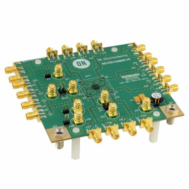
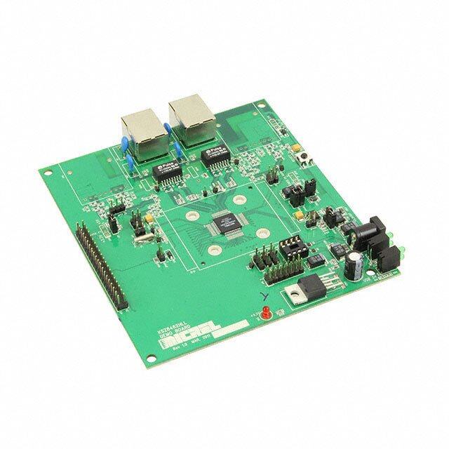
NB4N840MMNEVB Evaluation Board User's Manual for NB4N840M http://onsemi.com EVAL BOARD USER’S MANUAL Description The NB4N840M Evaluation Board was designed to applications. Each 2 x 2 crosspoint switch can fan−out provide a flexible and convenient platform to quickly and/or multiplex up to 3.2 Gb/s data and 2.7 GHz clock evaluate, characterize and verify the performance and signals. operation of the NB4N840M dual 2 x 2 Crosspoint Switch. Internally terminated differential CML inputs accept This user’s manual provides detailed information on the AC−coupled LVPECL (Positive ECL) or direct coupled board’s contents, layout and use. The manual should be used CML signals. By providing internal 50 (cid:2) input and output in conjunction with the NB4N840M data sheet which termination resistor, the need for external components is contains full technical details on device specifications and eliminated and interface reflections are minimized. operation. Differential 16 mA CML outputs provide matching internal The NB4N840M is a high−bandwidth fully differential 50 (cid:2) terminations, and 400 mV output swings when dual 2 x 2 crosspoint switch with CML inputs/outputs that externally terminated, 50 (cid:2) to V . CC is suitable for applications such as SDH/SONET DWDM Single−ended LVCMOS/LVTTL SEL inputs control the and high speed switching. Fully differential design routing of the signals through the crosspoint switch which techniques are used to minimize jitter accumulation, makes this device configurable as 1:2 fan−out, repeater or crosstalk, and signal skew, which make this device ideal for 2x2 crosspoint switch. The device is housed in a low profile loop−through and protection channel switching 5 x 5 mm 32−pin QFN package. Figure 1. NB4N840M Evaluation Board © Semiconductor Components Industries, LLC, 2012 1 Publication Order Number: February, 2012 − Rev. 2 EVBUM2078/D
NB4N840MMNEVB Board Features Power Supply • Fully assembled evaluation board • Accommodates the electrical characterization of the NB4N840M in the QFN32 package +3.3 V • + − Equal length input and output data lines to minimize skew • Selectable jumpers VCC GND • Single + 3.3 V supply This Evaluation Board Manual Contains +3.3 V • Information on the NB4N840M Evaluation Board • Appropriate Lab Setup Details Figure 2. Power Supply Connections • Evaluation Board Layout Step 3: Input Connections • Bill of Materials DAn and DBn require CML drive levels and provide internal 50 (cid:2) to V termination resistors to eliminate CC Setup for Measurements external components and minimize reflections. Ensure that the CML devices driving these inputs are not redundantly Step 1: Basic Equipment • terminated. Signal Generator • Oscilloscope • Table 2. Input Connectors Power Supply • Inputs Board Connector Voltmeter • Matched High−Speed Cables with SMA Connectors DA0 J13 DA0 J14 Step 2: Power Supply Connections DA1 J15 + 3.3 V must be provided to the board for V . CC DA1 J16 Table 1. Power Supply Connections DB0 J3 Supply Value Connector DB0 J4 VCC + 3.3 V J21 DB1 J1 GND 0 V J22 DB1 J2 Step 4: Control and Select Pins Jumpers JP1, JP2, JP5, and JP6 select the input signals for channel A and B outputs. Jumpers JP3, JP4, JP7, and JP8 enable the output drivers for channel A and B (refer to Table3 for output routing). Table 3. Output Routing ROUTING CONTROLS OUTPUT CONTROLS OUTPUT SIGNALS SELA0 / SELB0 SELA1 / SELB1 ENA0 / ENA1 ENB0 / ENB1 Signal at Signal at JP6 / JP2 JP5 / JP1 JP7 / JP8 JP3 / JP4 QA0 / QB0 QA1 / QB1 L L H H DA0 / DB0 DA0 / DB0 L H H H DA0 / DB0 DA1 / DB1 H L H H DA1 / DB1 DA0 / DB0 H H H H DA1 / DB1 DA1 / DB1 X X L L Power Down Power Down http://onsemi.com 2
NB4N840MMNEVB (J13) DA0 CML 0 QA0 (J12) (J14) DA0 CML 1 QA0 (J11) ENA0 (JP7) SELA0 (JP6) 0 QA1 (J10) (J15) DA1 CML CML 1 QA1 (J9) (J16) DA1 ENA1 (JP8) SELA1 (JP5) (J3) DB0 CML 0 QB0 (J6) (J4) DB0 CML 1 QB0 (J5) ENB0 (JP3) SELB0 (JP2) 0 QB1 (J8) (J1) DB1 CML 1 CML QB1 (J7) (J2) DB1 ENB1 (JP4) SELB1 (JP1) Figure 3. NB4N840M Evaluation Board Connector Configuration Step 5: Output Connections 2. Monitoring CML Outputs with High−Impedance The CML outputs, QAn and QBn, must be AC−coupled Oscilloscope Inputs to a 50 (cid:2) termination (100 (cid:2) differential) load. On−board a.Leave the coupling capacitors in series with the 100−(cid:2) differential terminations are provided to reduce outputs. noise on outputs that are not used. Connect the QAn/QBn b.Make sure the differential load resistors are on all the CML outputs to the oscilloscope with equally matched outputs (R9–R12). cables. 1. Monitoring One or More CML Outputs with 50 (cid:2) Table 4. Output Connectors Oscilloscope Inputs a.Leave the coupling capacitors in series with the Outputs Board Connector outputs. QA0 J12 b.Remove the associated 100 (cid:2) differential load QA0 J11 resistors from the evaluation board on the outputs QA1 J10 (R9–R12). c.It is important to remove the 100 (cid:2) resistor on the QA1 J9 output monitored, otherwise the load impedance will QB0 J6 not match the characteristic impedance of the line QB0 J5 and the resulting reflections will cause a degradation QB1 J8 in the output signal quality. d.If you are observing a single−ended output, balance QB1 J7 the other half with a 50 (cid:2) termination to ground (through the AC−coupling capacitor). http://onsemi.com 3
NB4N840MMNEVB VCC VCC L1 4.7 (cid:3)H C3 C4 C5 C6 C23 C24 C1 C2 0.1 (cid:3)F 0.1 (cid:3)F 0.1 (cid:3)F 0.1 (cid:3)F 0.1 (cid:3)F 0.1 (cid:3)F 33 (cid:3)F 2.2 (cid:3)F vcc C11 0.1 (cid:3)F J16 JP8 JP7 JP6 0.1 (cid:3)F C12 J15 JP5 0.1 (cid:3)F C13 J14 R8 R7 R6 R5 1 k(cid:2) 1 k(cid:2) 1 k(cid:2) 1 k(cid:2) 0.1 (cid:3)F J13 32 31 30 29 28 27 26 25 C14 J1 1 1 1 0 0 0 0 1 A A A A A A A A C7 N D D N L D D L JP4 0.1 (cid:3)F 1 ENB1E E SE SE GND 24 0C.11 (cid:3)5F J12 C8 J2 0.1 (cid:3)F 2 DB1 VCC 23 VCC 1 2 3 22 DB1 QA0 R9 C16 100 (cid:2) 0.1 (cid:3)F J11 4 21 JP3 ENB0 QA0 NB4N840M 1 5 20 VCC 2 JP2 SELB0 VCC C17 J3 0.1 (cid:3)F 6 19 J10 DB0 QA1 1 C9 7 18 2 0.1 (cid:3)F DB0 QA1 R10 8 17 100 (cid:2) C18 JP1 J4 C10 SELB1GND VCC QB0 QB0 VCC QB1 QB1 VCC VCC VCC 0.1 (cid:3)1F 2J9 0.1 (cid:3)F 9 10 11 12 13 14 15 16 C29 C31 1 Rk(cid:2)1 1R k2(cid:2) 1 Rk(cid:2)3 1R k4(cid:2) VCC VCC VCC J1710.1 (cid:3)F 0.1 (cid:3)F1J18 R12 R11 2 2 100 (cid:2) 100 (cid:2) C22 C21 C20 C19 0.1 (cid:3)F 0.1 (cid:3)F 0.1 (cid:3)F C30 C27 1 1 0.1 (cid:3)F 1 1 J1910.1 (cid:3)F 0.1 (cid:3)F1J20 J5 J6 J7 J8 2 2 2 2 2 2 Figure 4. Evaluation Board Schematic http://onsemi.com 4
NB4N840MMNEVB Table 5. BILL OF MATERIALS Manufacturer Part No. Ref. Number Qty Description Manufacturer (Notes 1, 2) R1 – R8 8 1 k(cid:2) ±1%, 0402, Resistors Multicomp MC0402WGF1001TCE−TR R9 – R12 4 100 (cid:2) ±1%, 0402, Resistors Multicomp MC0402WGF1000TCE−TR C1 1 33 (cid:3)F ±10%, size “D”, Tantalum Capacitor Kemet T491D336K016AT C2 1 2.2 (cid:3)F ±10%, size “C”, Tantalum Capacitor Kemet T491C225K035AT C3 – C24, C27, 26 0.1 (cid:3)F ±10%, 0402, Ceramic Capacitors Kemet C0402C104K4RAC−TU C29 – C31 L1 1 4.7 (cid:3)H Inductor Coilcraft DT3316P−472MLB U1 1 32 pin QFN ON Semiconductor NB4N840MMNG J1 – J20 20 SMA Edge Mount Connectors Johnson 142−0701−851 JS1 – JS8 8 SMA Connectors Johnson 142−0701−201 J21, J22 2 Test Point Jacks JP1 – JP8 8 1x2 Pin Headers, (0.1 inch pitch) SPC SPC20485 JP1 – JP8 8 Shunts SPC SPC19809 1. Specified parts are RoHS−compliant. 2. Only RoHS−compliant equivalent parts may be substituted. Board Lay−Up This board is implemented in four layers and provides a high bandwidth 50 (cid:2) controlled impedance environment. The pictures in Figures 5 through 9 show views of the four layers of the evaluation board. Board material is FR4. Top Silkscreen Top Soldermask Top Plating 01 Cu = 1/2 oz, 0.0007 Top Metal Dielectric 0.014 0 1 02 Cu = 1/2 oz, 0.0007 Plane 0 ± 0. Adjust 2 6 03 Cu = 1/2 oz, 0.0007 Plane 0 0. Dielectric 0.014 04 Cu = 1/2 oz, 0.0007 Bottom Metal Bottom Plating Bottom Soldermask Bottom Silkscreen Figure 5. Evaluation Board Lay−Up http://onsemi.com 5
NB4N840MMNEVB Figure 6. NB4N840MMN Evaluation Board Top (Component) Layer Figure 7. Ground Layer http://onsemi.com 6
NB4N840MMNEVB Figure 8. Power Layer Figure 9. Bottom Layer http://onsemi.com 7
NB4N840MMNEVB ON Semiconductor and are registered trademarks of Semiconductor Components Industries, LLC (SCILLC). SCILLC reserves the right to make changes without further notice to any products herein. SCILLC makes no warranty, representation or guarantee regarding the suitability of its products for any particular purpose, nor does SCILLC assume any liability arising out of the application or use of any product or circuit, and specifically disclaims any and all liability, including without limitation special, consequential or incidental damages. “Typical” parameters which may be provided in SCILLC data sheets and/or specifications can and do vary in different applications and actual performance may vary over time. All operating parameters, including “Typicals” must be validated for each customer application by customer’s technical experts. SCILLC does not convey any license under its patent rights nor the rights of others. SCILLC products are not designed, intended, or authorized for use as components in systems intended for surgical implant into the body, or other applications intended to support or sustain life, or for any other application in which the failure of the SCILLC product could create a situation where personal injury or death may occur. Should Buyer purchase or use SCILLC products for any such unintended or unauthorized application, Buyer shall indemnify and hold SCILLC and its officers, employees, subsidiaries, affiliates, and distributors harmless against all claims, costs, damages, and expenses, and reasonable attorney fees arising out of, directly or indirectly, any claim of personal injury or death associated with such unintended or unauthorized use, even if such claim alleges that SCILLC was negligent regarding the design or manufacture of the part. SCILLC is an Equal Opportunity/Affirmative Action Employer. This literature is subject to all applicable copyright laws and is not for resale in any manner. PUBLICATION ORDERING INFORMATION LITERATURE FULFILLMENT: N. American Technical Support: 800−282−9855 Toll Free ON Semiconductor Website: www.onsemi.com Literature Distribution Center for ON Semiconductor USA/Canada P.O. Box 5163, Denver, Colorado 80217 USA Europe, Middle East and Africa Technical Support: Order Literature: http://www.onsemi.com/orderlit Phone: 303−675−2175 or 800−344−3860 Toll Free USA/Canada Phone: 421 33 790 2910 Fax: 303−675−2176 or 800−344−3867 Toll Free USA/Canada Japan Customer Focus Center For additional information, please contact your local Email: orderlit@onsemi.com Phone: 81−3−5817−1050 Sales Representative http://onsemi.com EVBUM2078/D 8
Mouser Electronics Authorized Distributor Click to View Pricing, Inventory, Delivery & Lifecycle Information: O N Semiconductor: NB4N840MMNEVB