ICGOO在线商城 > 传感器,变送器 > 运动传感器 - 加速计 > MXP7205VW
- 型号: MXP7205VW
- 制造商: MEMSIC
- 库位|库存: xxxx|xxxx
- 要求:
| 数量阶梯 | 香港交货 | 国内含税 |
| +xxxx | $xxxx | ¥xxxx |
查看当月历史价格
查看今年历史价格
MXP7205VW产品简介:
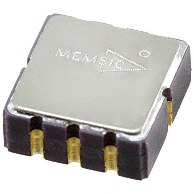
ICGOO电子元器件商城为您提供MXP7205VW由MEMSIC设计生产,在icgoo商城现货销售,并且可以通过原厂、代理商等渠道进行代购。 MXP7205VW价格参考。MEMSICMXP7205VW封装/规格:运动传感器 - 加速计, Accelerometer X, Y or X, Z Axis ±5g 29Hz 8-LCC。您可以下载MXP7205VW参考资料、Datasheet数据手册功能说明书,资料中有MXP7205VW 详细功能的应用电路图电压和使用方法及教程。
| 参数 | 数值 |
| 产品目录 | |
| 描述 | IC ACCELEROMETER XY AXIS LCC8 |
| 产品分类 | 加速计 |
| 品牌 | Memsic Inc |
| 数据手册 | |
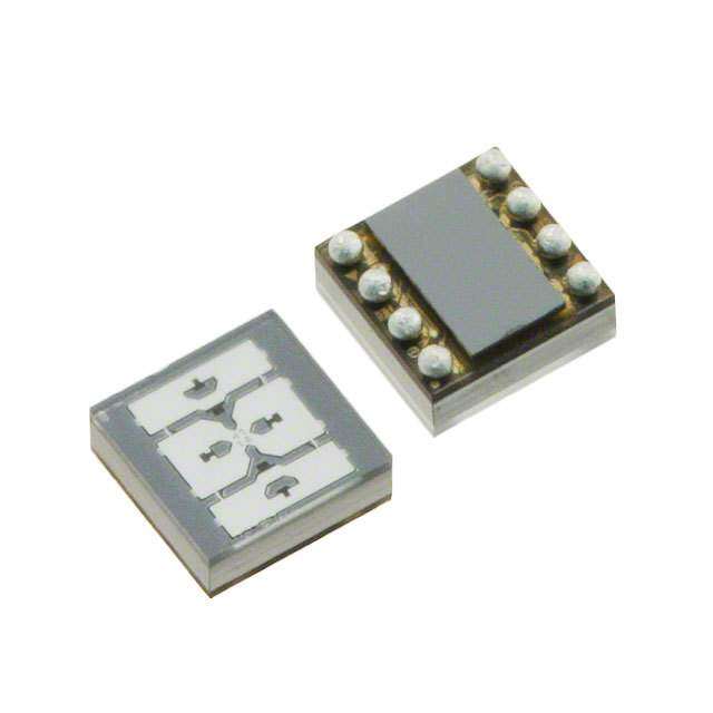
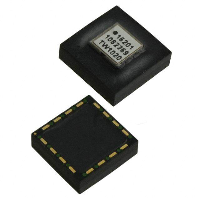
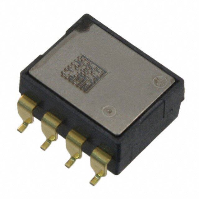
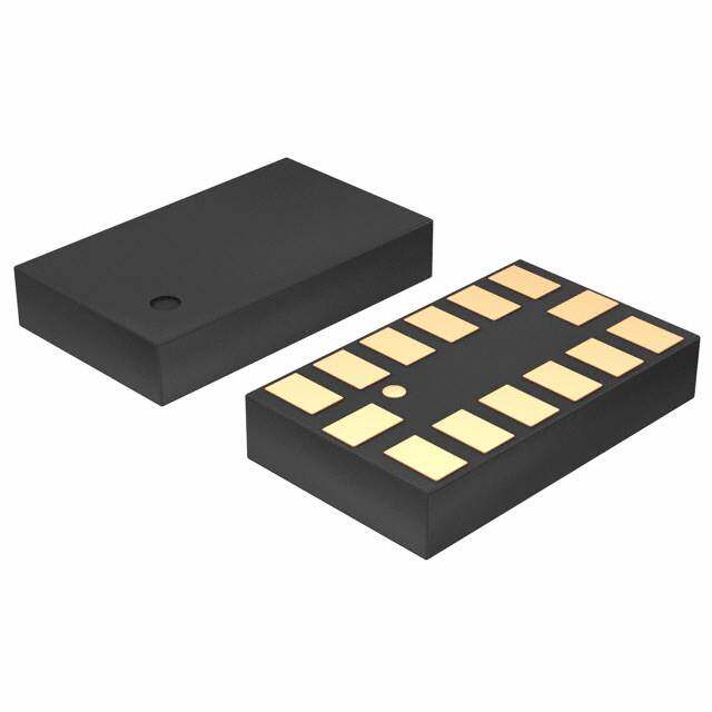
| 产品图片 |
|
| 产品型号 | MXP7205VW |
| rohs | 无铅 / 符合限制有害物质指令(RoHS)规范要求 |
| 产品系列 | - |
| 供应商器件封装 | 8-LCC |
| 其它名称 | 1267-1015-1 |
| 加速度范围 | ±5g |
| 安装类型 | 表面贴装 |
| 封装/外壳 | 8-LCC |
| 带宽 | 29Hz |
| 接口 | SPI |
| 标准包装 | 1 |
| 灵敏度 | 800LSB/g |
| 电压-电源 | 4.5 V ~ 5.25 V |
| 轴 | X,Y |
| 输出类型 | SPI |



- 商务部:美国ITC正式对集成电路等产品启动337调查
- 曝三星4nm工艺存在良率问题 高通将骁龙8 Gen1或转产台积电
- 太阳诱电将投资9.5亿元在常州建新厂生产MLCC 预计2023年完工
- 英特尔发布欧洲新工厂建设计划 深化IDM 2.0 战略
- 台积电先进制程称霸业界 有大客户加持明年业绩稳了
- 达到5530亿美元!SIA预计今年全球半导体销售额将创下新高
- 英特尔拟将自动驾驶子公司Mobileye上市 估值或超500亿美元
- 三星加码芯片和SET,合并消费电子和移动部门,撤换高东真等 CEO
- 三星电子宣布重大人事变动 还合并消费电子和移动部门
- 海关总署:前11个月进口集成电路产品价值2.52万亿元 增长14.8%


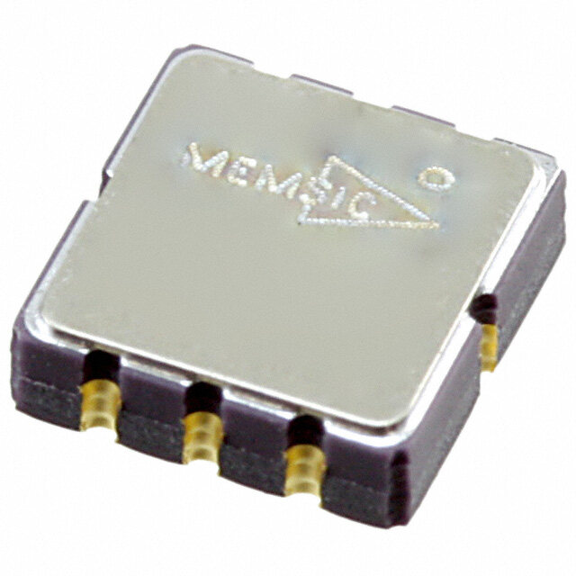


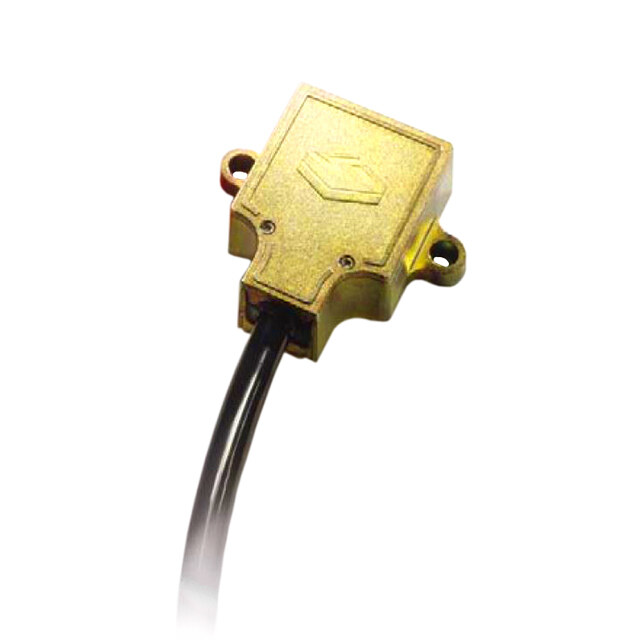
PDF Datasheet 数据手册内容提取
Low Cost ±5 g Dual-Axis Accelerometer with SPI Interface Automotive Grade MXP7205VW FEATURES VDA Dual axis accelerometer fabricated on a single CMOS IC TEMP Monolithic design with mixed mode signal processing Zero-g temperature stability better than ±30mg from –40C to FM RCeognitsrtoelr OInstceirllnaatolr VRoelfteargeence TeSmenpseorarture 105C CLK CLK Vref TEMP Sensitivity temperature compensation better that ±3% from -40C to 105C HCoenattreorl GCaoianr sAedj. FiAndej .Gain ± 5g dynamic range, 800LSB/g sensitivity 29Hz bandwidth X axis TCeommpp. A/D LoFwil tPerass On Demand Self Test >4.5500,V00 t0o g5 .s2h5oVc ski nsgulrev isvuapl pralyti nogp eration VDD GCCaoiaLnrK sAedj. CFLAiKndejT .GEaMinP CLK CLK IntSerPfaIce SSMCSOBKSI MISO Small surface mount package, 5.5mm x 5.5mm x 2.7mm XZ or XY mounting Y axis TCeommpp. A/D LoFwil tPerass RoHS compliant AcSceenlesroartion CLK CLKTEMP CLK CLK GND AUTOMOTIVE APPLICATIONS • Vehicle Stability Control MXP7205VW FUNCTIONAL BLOCK DIAGRAM • Roll Over Detection • Electronic Parking Break – Hill Start Assist • Headlight Leveling and Steering GENERAL DESCRIPTION The MXP7205VW is a low cost, dual axis accelerometer MEMSIC’s accelerometer technology allows for designs built on a standard, submicron CMOS process. It measures from ±1 g to ±70 g with custom versions available above acceleration with a full-scale range of ±5g and a sensitivity ±70 g. It can measure both dynamic acceleration (e.g., of 800LSB/g with 14bits operation mode and 50LSB/g with vibration) and static acceleration (e.g., gravity). 10bits operation mode. The design is based on heat convection and requires no The MXP7205VW provides an SPI interface. solid proof mass. This eliminates stiction, particle, and The typical noise floor is 0.6mg / Hz , allowing signals inherent resonant frequency problems associated with competitive devices and provides shock survivability to below 1mg to be resolved at 1Hz bandwidth. The inherent greater that 50,000g, leading to significantly lower failure 3dB roll off of the device is 29Hz providing immunity to rates and lower loss due to handling during assembly and at and attenuation of higher frequency vibrations present in customer field application. automotive applications. The MXP7205VW is packaged in a hermetically sealed Due to the standard CMOS structure of the MXP7205VW, additional circuitry can easily be incorporated into custom LCC surface mount package (5.5 mm x 5.5 mm x 2.7 mm versions for high volume applications. Contact MEMSIC’s height), and the package can be used for either XY and XZ local office for more information. sensing, its operation temperature is -40°C to +105°C. Information furnished by MEMSIC is believed to be accurate and reliable. ©MEMSIC, Inc. However, no responsibility is assumed by MEMSIC for its use, nor for any One Technology Drive, Suite 325, Andover, MA01810, USA infringements of patents or other rights of third parties, which may result from Tel: +1 978 738 0900 Fax: +1 978 738 0196 its use. No license is granted by implication or otherwise under any patent or www.MEMSIC.com patent rights of MEMSIC. MEMSIC MXP7205VW Rev.C Page 1 of 11 8/2/2011
MXP7205VW SPECIFICATIONS (Measurements @ 25°C, 14bits operation mode, Acceleration = 0 g unless otherwise noted; V = V =5.0V unless otherwise specified) DD DA PARAMETER Conditions MIN TYP MAX UNITS Full scale ranges -5 5 g Nominal Sensitivity 14bits operation mode 800 LSB/g 10bits operation mode 50 LSB/g Initial @ 25°C -3 0 +3 % Sensitivity drift Initial -40°C to +105°C -3 +3 % Sensitivity drift Include Aging -4 0 +4 % -40°C to +105°C Cross Axis Sensitivity 2.0 % Non-Linearity (best straight line) FSR=10g 1.0 %FSR Zero g Output Offset 2's complement output 0 LSB Initial @ 25°C -60 0 +60 mg Zero g Output Temperature Drift Initial -40°C to +105°C -30 +30 mg 1.0 mg/°C Zero g Output Temperature Drift Include Aging -60 0 +60 mg -40°C to +105°C Total Offset Drift Due to -40°C to +105°C with 80 mg Temperature 1 2.5°C/min Temp Ramp (max-min) -20°C to +80°C with 40 mg 2.5°C/min Temp Ramp (max-min) 0°C to +60°C with 50 mg 2.5°C/min Temp Ramp (max-min) Selftest Signal X-axis +2.5 g Y/Z-axis -2.5 g Selftest Signal Tolerance 25°C -5 +5 % Selftest Signal Drift (0g input) -40°C to +105°C -5 +5 % -40°C to +105°C, include -8 +8 % aging Selftest Signal Rise/Fall Time 20 mS Frequency Response 26 29 32 Hz Phase Delay 0 to 1KHz 10 12 mS Recover Time From Overload Input 10g, 1mS shock 2 mS 10000g, 0.5mS half sine 10 mS shock Input Referred Noise Density -40°C to +105°C, within 0.5 1.5 mg/sqrtHz 29Hz RMS Output Noise No external filtering, 25°C 3.5 5.5 mg RMS No external filtering 11 mg RMS -40°C to +105°C Power up time 2 200 300 mS Operation Power Supply Range 4.5 5.0 5.25 V Power consumption @5V 3.5 4.5 mA Operation Temperature Range -40 105 °C Note: 1: Requirements can be met by characterization of 3lots x 30 parts per lot, not 100% test in production. 2: Output settled to within +/-17mg of the final value. MEMSIC MXP7205VW Rev.C Page 2 of 12 8/2/2011
DIGITAL INTERFACE SYMBOL PARAMETER CONDITIONS MIN MAX UNITS VIH High Level Input Voltage 0.7 x VDD V VIL Low Level Input Voltage 0.3 x VDD V Vhys Hysteresis (SCK, SSB, DI/MOSI) 0.1 0.4 V VOH High Level Output (MISO) Iout = 0.2mA VDD-0.4 V VOL Low Level Output (MISO) Iout = ─0.5mA 0.4 V Rin1 Pull-down resistance 100 200 kΩ (SCK, DI/MOSI) Rin2 Pull-down resistance (FM) 30 50 kΩ IPU Pull-up Current (SSB) VDD=4.5-5.5V 10 50 μA (SPI mode) CL Load Capacitance (MISO) 80 pF SYMBOL PARAMETER CONDITIONS MIN TYP MAX UNITS SPI Operating Frequency 8.08 MHz Data Register Update Rate 800 KHz SPI Communication Startup Time 1 ms td1 SCK High Time .5 x td3 - 13 ns td2 SCK Low Time .5 x td3 - 13 ns td3 SCK Period 123.7 ns tr, tf SCK Rise/Fall Time 0.1xVDD - 13 ns 0.9xVDD td4 Data Input (MOSI) Setup Time 37 ns td5 Data Input (MOSI) Hold Time 49 ns td6 Data Out (MISO) Access Time 43 ns td7 Data Out(MISO) Valid After SCK 30 ns td8 Data Output (MISO) Lag Time 0 ns td9 Data Output (MISO) Disable Time 750 ns td10 Enable (SSB) Lead Time .5 x td3 ns td11 Enable (SSB) Lag Time .5 x td3 ns td12 Sequential Transfer Delay 1.5 x td3 ns SPI Timing MEMSIC MXP7205VW Rev.C Page 3 of 12 8/2/2011
ABSOLUTE MAXIMUM RATINGS* Note: The MEMSIC logo’s arrow indicates the +Z sensing Supply Voltage (V , V ) ¹ ……………...-0.5 to +7.0V direction of the device. DD DA Small circle indicates pin one (7). Storage Temperature ……….…………-55°C to +150°C Storage Pressure…………………………………1,378 kPa ESD Compliance: Acceleration (any axis, Un-powered for 0.5 msec)..50,000 g The MXP7205VW sensor is in compliance with the following Acceleration (any axis, Powered for 0.5 msec)… 10,000 g ESD standards: Output Short Circuit Duration, any pin to common…….Indefinite HBM class H2 per AEC-Q100-002 Rev. E MM class M2 per AEC-Q100-003 Rev. E *Stresses above those listed under Absolute Maximum Ratings may cause permanent damage to the device. This is a stress rating only; the functional operation of the device at these or any other conditions above those indicated in the operational sections of this specification is not implied. Exposure to absolute maximum rating conditions for extended periods may affect device reliability. XY Sensing: ¹ Exposure for up to 60 minutes to absolute maximum ratings for supply voltages will not affect device reliability. 7 6 Ordering Guide Model Package Style MXP7205VW LCC-8 SMD* * Parts are shipped in tape and reel packaging. +Z 8 5 Pin Description: LCC Package Pin Name Description 1 MISO Master In - Slave Out 2 VDA Analog Supply 1 2 3 4 3 V Digital Supply, V and V DD DA DD +X must be the same voltage 4 FM Factory mode (for factory test (Top View, do not scale) only). Connect to VSS 5/J SCK Clock Input Note: Small circle indicates pin seven (7). 6/M SSB Slave Select Bar (active low) 7/L VSS Ground XZ Sensing: 8/K MOSI Master Out - Slave In M L K J Caution ESD (electrostatic discharge) sensitive device. X=0 Z=800 1 2 3 4 +X (Bottom View, do not scale) X=800 TOP VIEW X=-800 Z=0 (Not to Scale) Z=0 X=0 Z=0 X=0 Z=-800 EARTH’S SURFACE MEMSIC MXP7205VW Rev.C Page 4 of 12 8/2/2011
MOSI – This pin serves as the Master Out Slave In (MOSI) THEORY OF OPERATION SPI function. The MOSI signal is the serial input data to the MXP7205VW from the external SPI controller, such as The MEMSIC device is a complete dual-axis acceleration SPI control register load commands or requests for output measurement system fabricated on a monolithic CMOS IC data. . process. The device operation is based on heat transfer by natural convection and operates like other accelerometers SCK – This pin is the SPI clock signal and is used to having a proof mass except it is a gas in the MEMSIC transfer data between the MXP7205VW and an external sensor. controller via the MOSI and MISO pins. A single heat source, centered in the silicon chip is SIGNAL PATH FREQUENCY RESPONSE suspended across a cavity. Equally spaced aluminum/polysilicon thermopiles (groups of The frequency response of the MXP7205VW is primarily thermocouples) are located equidistantly on all four sides of determined by the thermal sensor characteristics and a the heat source (dual axis). Under zero acceleration, a digital lowpass filter included in the signal path to eliminate temperature gradient is symmetrical about the heat source, quantization noise and limit thermal noise bandwidth. The so that the temperature is the same at all four thermopiles, sensor is modelled as a two pole lowpass filter, with real causing them to output the same voltage. poles located nominally at 40 Hz and 85 Hz. The lowpass filter is a second order Butterworth filter with a 3 dB cutoff Acceleration in any direction will disturb the temperature frequency of nominally 44 Hz. Sensor poles have a profile, due to free convection heat transfer, causing it to be tolerance of approximately ±10%, and the Butterworth filter asymmetrical. The temperature, and hence voltage output cutoff frequency has a tolerance of approximately ±5%. of the four thermopiles will then be different. The differential voltage at the thermopile outputs is directly The nominal complex transfer function of the signal path is proportional to the acceleration. There are two identical given by: acceleration signal paths on the MXP7205VF, one to measure acceleration in the x-axis and one to measure 1 1 1 H(f)= • • acceleration in the y/z-axis. For more details visit the MEMSIC website at www.MEMSIC.com for a 1+ j⎜⎛ f ⎟⎞ 1+ j⎜⎛ f ⎟⎞ 1−⎜⎛ f ⎟⎞2 + j 2⎜⎛ f ⎟⎞ picture/graphic description of the free convection heat ⎝40⎠ ⎝85⎠ ⎝44⎠ ⎝44⎠ transfer principle. Plots of the amplitude (in dB, relative to DC sensitivity) PIN DESCRIPTIONS and phase response (in degrees) of the signal path for typical, minimum, and maximum sensor and filter pole V – This is the digital power supply for the DD frequencies are shown below. MXP7205VW. This pin supplies current to the heater element and digital circuitry. The DC voltage should be between 4.5V and 5.25V. V – This is the analog power supply. This pin supplies DA current to the analog circuitry. The DC voltage should be equal to the voltage supplied to the V pin. DD VSS – This is the ground pin for the MXP7205VW. FM – Factory Mode for factory use only, connect to VSS. MISO – This pin serves as the Master In Slave Out (MISO) SPI function. The MISO signal is the serial output data sent from the MXP7205VW to the external SPI controller, such Signal Path Amplitude Response as acceleration output data and status information. SSB – This pin serves as the Slave Select Bar (SSB) SPI function. When SSB is high, communication with the SPI is disabled; when SSB is low, communication is enabled, and data can be exchanged between the MXP7205VW and the external SPI controller. MEMSIC MXP7205VW Rev.C Page 5 of 12 8/2/2011
advantage in generating and measuring an accurate ST signal. Note: ST means Self Test, TC means Temperature Compensation The recommended method for verifying ST amplitude is as follows: 1. Set the control register bit TC=1 to disable TC. 2. Read acceleration output on the desired channel(s) (read through the SPI port) -- call this Out1. 3. Set control bit ST=1, leaving TC=1, which disables TC Signal Path Phase Response and activates ST. 4. Read acceleration output on the same channel(s) -- call this Out2. 5. Subtract (Out2─Out1). This is the ST signal amplitude. SELF-TEST DESCRIPTION 6. Set ST=0 and TC=0, returning the accelerometer to normal mode. The gas law governs the change in sensitivity over temperature. Using the above method, the presence of a real constant All thermal accelerometers display the same sensitivity acceleration stimulus does not affect the ST amplitude, change with temperature. The sensitivity change depends provided that the acceleration plus self-test signal is not so on variations in heat transfer that are governed by the laws large that the signal path is saturated. of physics. Manufacturing variations do not influence the sensitivity change, so there are no unit-to-unit differences in Note1: When the temperature compensation is disabled and sensitivity change. The sensitivity change is governed by self-test is enabled. Self-test follows different gas law from the following equation (and shown in Figure 1 in °C): sensitivity temperature dependence. It changes much smaller than sensitivity; this is why the temperature S x T2.8 = k x S x T2.8 compensation is not done on self-test conditions. i i f f where Si is the sensitivity at any initial temperature Ti, and Note2: Initial offset monitoring is a much better and Sf is the sensitivity at any other final temperature Tf with reliable method to ensure sensor integrity, since it is ultra the temperature values in °C, k is the ratio between sensitive to sensor structure defect and damage. As long as uncompensated sensitivity and compensated sensitivity at initial offset is within specification the sensor is functioning 25°C. correctly. The sensor structure for the Thermal technology is 2.5 guaranteed to fall outside the specified initial zero g offset malized) 2.0 pIna rmamosett ecrass eifs tthheis s wenisllo rre issu dlta imn aegiethde or rs itghnearml poaptihle s aist ufraaitliionng . nor 1.5 or in the Hardware Error (HE) status bit being set. nsitivity ( 01..50 Se PCB LAYOUT AND FABRICATION SUGGESTIONS 0.0 Reference figure and the notes below for recommendations -40 -20 0 20 40 60 80 100 Temperature (C) on connecting a power source to the MEMSIC device and PCB fabrication. Thermal Accelerometer Sensitivity A SPI function has been included for digital serial communication with an external host microprocessor. The device includes a control register for activating various operating and test modes. This control register includes a TC bit and an ST bit, which can be written via the SPI port. Setting TC=1 disables the TC function; setting ST=1 activates the ST function. The ability to control the TC and ST functions independently provides a significant MEMSIC MXP7205VW Rev.C Page 6 of 12 8/2/2011
C1 in the thermal sensor through the VDD and VSS pins. Power The nominal heater resistance is about 500ohm, and nominal heater power is about 7.5 mW. With VDD=5.0V, peak current in the heater element is approximately 10 mA. An internal switching regulator 7 VSS SSB 6 ensures that heater power remains essentially constant with temperature and supply voltage variations. This regulator uses Pulse Width Modulation (PWM) and operates at a fundamental frequency of 1.6 MHz. At VDD=5V, the PWM regulator duty cycle is nominally +Z 8 MOSI SCK 5 15-20%. The bypass capacitor should be able to deliver the required charge during each regulator switching period to ensure low supply noise. 3. Robust low inductance ground and supply wiring MISO VDA VDD FM should be used. 4. Care should be taken (like isolated rings and planes, 1 2 3 4 signal route out perpendicular to the external thermal +X gradient) to ensure there is “thermal symmetry” on the PCB immediately surrounding the MEMSIC device and that there is no significant heat source nearby. This will minimize any errors in the measurement of PCB Layout acceleration. Notes: 1. C = 1.0μF 1 2. The bypass capacitance should be placed near the VDD and VSS pins to ensure low noise performance and accurate outputs. The predominant transient currents on the MXP7205VW are supplied to the heater element MEMSIC MXP7205VW Rev.C Page 7 of 12 8/2/2011
SERIAL PERIPHERAL INTERFACE PROTOCOL The Serial Peripheral Interface (SPI) is a synchronous serial communication subsystem. The SPI described here is a 16-bit variation of the original 8-bit design. There are four pins associated with the SPI: 1. SCK (serial clock), 2. MISO (master in/ slave out), 3. MOSI (master out/ slave in), and 4. SSB (slave select bar). Internal to each device on the SPI bus is a 16-bit shift register. Devices can operate in either a master or slave role. There can only be one master on the SPI bus at any given time. The pins MISO, MOSI, and SCK are tied together for all devices on the bus. To initiate a data transfer, the master device pulls SSB low on the slave device that it wishes to communicate with. Internal to the slave device this accomplishes two things: 1. It allows SCK (generated by the master) to pass through to the shift register, and 2. It enables output MISO (all unselected slave devices on the bus will have MISO tri-stated). During an SPI transfer, a 16-bit word is shifted out of MISO, while a different 16-bit word is simultaneously shifted into MOSI, synchronous with clock SCK (for the master device, the roles of MISO and MOSI are reversed). Another way to view the transfer is that a 16-bit shift register in the master, and another 16-bit shift register in the slave are connected as a circular 32-bit shift register. When a transfer occurs, this distributed shift register is shifted 16 bit positions; thus the data words in the master and slave are effectively exchanged. The SPI on the MXP7205VW is designed to operate only in the slave mode. It uses the protocol CPHA = 0, CPOL = 0, that is, data changes on MOSI and MISO on the falling edge of SCK, and is clocked into the shift register on the rising edge of SCK. When the MXP7205VW is selected as the slave device, 16-bits of data, MSB first, are simultaneously shifted from the master to the slave, and from the slave to the master on the 16 rising edges of SCK. After the 16th rising edge of SCK, the slave shift register will contain the 16-bit word that was transferred from the master. Internal to the MXP7205VW there is a 16-bit bus that serves both as the address bus and the data bus. Immediately after the 16th rising edge of SCK, the internal bus will be driven by the shift register outputs, and will be used as the address bus. When SCK falls, the address on the internal bus will be latched into the address decoders. During the time between the last falling edge of SCK and the next falling edge of SSB, data will be placed on the internal bus in accordance with the instruction received by the address decoders. On the rising edge of SSB, the data on the internal bus will be latched into the appropriate register. The rising edge of SSB also signals the end of the data transfer. There are 2 types of data transfers supported by the MXP7205VW SPI: 1.Master reading the x and y/z channel MSB and LSB accelerometer output registers, and 2. Master reading and writing the MXP7205VW 8-bit control register. If bit 13, “SEN”, of the word written from the master to the MXP7205VW is hi, then the instruction is a read of an accelerometer output register. If bit 13 is low, then the instruction is either a read or write of the MXP7205VW control register. The protocol for reading the accelerometer output registers is shown in following tables Sensor Data Request (MOSI): MSB LSB 15 14 13 12 11 10 9 8 7 6 5 4 3 2 1 0 SQ1 SQ0 SEN SQ2 - - - - - - - - LC3 LC2 LC1 LC0 - - 1 - Accelerometer output LSB register, x-channel - - 0 0 - - 1 - Accelerometer output LSB register, y/z-channel - - 0 1 - - 1 - Accelerometer output MSB register, x-channel - - 1 0 - - 1 - Accelerometer output MSB register, y/z-channel - - 1 1 Sensor Data Request Name Bit Position Definition SQ2:SQ0 15,14,12 Sequence identifier - used for synchronizing samples SEN 13 SEN = 1, sensor data read; SEN = 0, control register read or write. LC3:LC0 3:0 Logical channel select 11:4 Not used for sensor data request. Sensor Data Request MOSI Bit Definition MEMSIC MXP7205VW Rev.C Page 8 of 12 8/2/2011
Sensor Data Response (MISO): MSB LSB 15 14 13 12 11 10 9 8 7 6 5 4 3 2 1 0 SQ2 SQ1 SQ0 P ST1 ST0 D9 D8 D7 D6 D5 D4 D3 D2 D1 D0 ↓ ↓ 0 0 Not Used 0 1 Sensor Data 1 0 Self-Test Data 1 1 1 ES1 ES0 Exception Status ↓ ↓ 0 0 Sensor Error Data 0 0 0 ND CNC HE ME DE 0 1 Not Used 1 0 Not Used 1 1 Reserved Sensor Data Response Notes: 1 The self-test data response, with ST1 = 1, ST0 = 0, will occur when the control register contains the values ST = 1 (self- test enabled), or TC = 1 (temperature compensation disabled). Sensor Data Response MISO Bit Definition Name Bit Position Definition SQ2:SQ0 15:13 Sequence identifier - used for synchronizing sensor samples P 12 Parity - Ensures odd parity for bits 15:0 of MISO ST1:ST0 11:10 Status - Identifies contents in D9:D0 of MISO (sensor data, self-test data, exception) ES1:ES0 9:8 Exception Status - Identifies contents of exception data (sensor error status) 7:5 Not used if ST1:ST0 = 11 ND 4 No Data - Not used. CNC 3 Conditions Not Correct - Set if attempt is made to read accelerometer data when chip is in power down. HE 2 Hardware Error - Set if heater control loop is out of regulation. ME 1 Reserved DE 0 Reserved D9:D0 9:0 Sensor Data - For ST1:ST0 = 01 or 10. Data is LSB justified, and MSB bits are padded with ‘0’ if data length is less than 10. Sensor Data Response MISO Bit Definition The error codes supported by the MXP7205VW when an attempt is made to read accelerometer data (SEN = 1), are CNC = 1, if the chip is in the power down state, and HE = 1, if the heater control loop is out of regulation. If self-test is activated when an attempt is made to read accelerometer data, this will be indicated by returning ST1:ST0 = 10. When reading accelerometer data, there are 4 modes of operation, defined by the settings of bits DAT1 and DAT0 in the MXP7205VW Control Register. The modes of operation for the different settings are given in following table. DAT1 DAT0 Definition 0 0 If the MSB or LSB register of either the x or y/z channel is read, then both the x and y/z channel outputs are frozen until the MSB and LSB of both the x and y/z channels are read. 0 1 If the MSB or LSB register of either the x or y/z channel is read, then that channel’s output is frozen until the other byte (either LSB or MSB) is read. 1 0 If the MSB register of either the x or y/z channel is read, then both the x and y/z channel outputs are frozen until the MSB of the other channel is read. 1 1 Channel outputs are continuously updated. Channel Output Modes of Operation The output of either the x or y/z channel is a 14-bit word. Since only 10-bits of data are available from a channel output read, two read cycles are required to obtain the full 14-bit data word. The 14-bit word can be considered to be stored in a Most Significant MEMSIC MXP7205VW Rev.C Page 9 of 12 8/2/2011
Byte (MSB) Register, which contains the 10 most significant bits, and a Least Significant Byte (LSB) Register, which contains the 4 least significant bits, right justified, with zeros inserted for the remaining 6 data bits. If a 14-bit output is desired, then the MSB and LSB register reads should be from the same output sample. Therefore, in the 14-bit output mode of operation (DAT1 = 0), the filter output will not be updated until both the MSB and LSB for that channel have been read. It may also be desirable to have a reading of both the x and y/z channel outputs corresponding to the same output sample. In that case, setting DAT0 = 0 will cause the filter outputs to be frozen, after a read of one of the channels, until both channels are read. A 10-bit mode of operation is also available. In this case, only the MSB register of the x and y/z channels are read. Setting DAT0 = 0 requires that both channels be read before the filter outputs are updated. When DAT1 = 1 and DAT0 = 1, the filter outputs are updated continuously. Data transfer format: 14bits operation mode 10bits operation mode LSB Hex g LSB Hex g 6144 1800 7.68 384 180 7.68 4000 0FA0 5 250 0FA 5 800 320 1 50 32 1 1 1 0.00125 1 1 0.02 0 0 0 0 0 0 -1 3FFF -0.00125 -1 3FF -0.02 -800 3CE0 -1 -50 3CE -1 -4000 3060 -5 -250 306 -5 -6144 2800 -7.68 -384 280 -7.68 The protocol for reading and writing to the control register is shown in following tables. Slave Data Request (MOSI): MSB LSB 15 14 13 12 11 10 9 8 7 6 5 4 3 2 1 0 OP1 OP0 SEN A4 A3 A2 A1 A0 D7 D6 D5 D4 D3 D2 D1 D0 ↓ ↓ 0 0 0 Not Used 0 1 0 Write Address Write Data 1 0 0 Read Address Don’t Care 1 1 0 Not Used Slave Data Request Name Bit Position Definition OP1:OP0 15:14 Opcode - Defines operation (Read, Write). SEN 13 SEN = 1, sensor data read; SEN = 0, control register read or write. A4:A0 12:8 Address - For read or write operation. D7:D0 7:0 Data - For write operation. Slave Data Request MOSI Bit Definition Slave Data Response (MISO): MSB LSB 15 14 13 12 11 10 9 8 7 6 5 4 3 2 1 0 - OP1 OP0 P ST1 ST0 ES1 ES0 D7 D6 D5 D4 D3 D2 D1 D0 ↓ ↓ 0 0 P 1 1 1 0 Error Data 0 0 0 0 0 SE RE DU 0 1 P 1 1 1 0 Slave Status - Responds with data just written 1 0 P 1 1 1 0 Read Data 1 1 P 1 1 1 0 - Slave Data Response MEMSIC MXP7205VW Rev.C Page 10 of 12 8/2/2011
Name Bit Position Definition OP1:OP0 14:13 Opcode - Identifies contents of Read or Write data in D9:D0 - copied from MOSI if request granted P 12 Parity - Ensures odd parity for bits 15:0 of MISO ST1:ST0 11:10 Status - Always ‘11’ for non-sensor response ES1:ES0 9:8 Exception Status - Always ’10’ for non-sensor response D7:D0 7:0 Read Data/Error Data/Status SE 2 SPI Error - Set if there is an incorrect number of SCK clock pulses during a data transfer frame RE 1 Request Error - Set to ‘1’ for illegal, or unknown requests DU 0 Data Unavailable - Not used Slave Response MISO Bit Definition Summary of MXP7205VW SPI protocol: If bit 13 (SEN) of the request is a ‘1’, then the data transfer is a read of one of the accelerometer output registers. Bits 15 (SQ1), 14 (SQ0), and 12 (SQ2) are the sequence bits. This field provides the system with a means of synchronizing the data samples received from the sensors. Bits 3:0 are the logical channel bits, LC3:LC0. These bits determine whether the x or y axis data is being read, and whether the MSB or LSB byte is being read. None of the other bits in the request have any meaning. If bit 13 (SEN) of the request is a ‘0’, then the data transfer is a write or read of the MXP7205VW control register. Bits 15 (OP1), and 14 (OP0) define whether the request is a write (OP1:OP0 = 01), or a read (OP1:OP0 = 10). Since the MXP7205VW has only one control register, the address bits in the request are irrelevant. All requests with SEN=0, are assumed to be directed to the 8-bit control register. The only other bits that have meaning, besides 15:13, for a slave data request, are the data bits 7:0, for the case of a write to the control register. The errors that are detected for a sensor data request are: 1. CNC = 1, chip is in power down state; and 2. HE = 1, heater control loop is out of regulation. If the number of SCK rising edges during a data transfer (period of time from the falling edge of SSB to the rising edge of SSB) is different from 16, then bit 2 (SE) will be set. If the request does not correspond to any of the requests defined in this specification, then bit 1 (RE) will be set. The remaining bits in the response, for these errors, will correspond to those given in the table of Slave Data Response. The response on MISO during the first command following a reset will be a slave data error response with RE = 1, DU = 1. MXP7205VW CONTROL REGISTER The MXP7205VW contains a single 8-bit control register. This register can be written to and read by the master device. The bit definitions are shown in following table, followed by a description of each control bit. MSB LSB 7 6 5 4 3 2 1 0 DAT1 DAT0 RFILT FTST1 FTST0 TC ST PD MXP7205VW Control Register DAT1:DAT0 - These 2 bits determine how the accelerometer output registers will be updated. RFILT - Writing this bit to a ‘1’ resets the digital filters for the x and y/z channels. The bit must be cleared for normal operation to resume. Can be used in the testing of the filters. While the digital filters are in reset (RFILT=1), the x and y acceleration outputs will be 0. FTST1:FTST0 - These bits are used to facilitate testing of the digital filter. The different modes of operation are described in following table. Both the x channel and y/z channel filters are affected in the same way. FTST1 FTST0 Definition 0 0 Normal operating mode MEMSIC MXP7205VW Rev.C Page 11 of 12 8/2/2011
0 1 Filter input comes from pattern generator with 25% pulse density. Expected Xout/Yout (Zout) values are ─3072. 1 0 Filter input comes from pattern generator with 50% pulse density. Expected Xout/Yout (Zout) values are 0. 1 1 Filter input comes from pattern generator with 75% pulse density. Expected Xout/Yout values are +3072. Digital Filter Test Modes TC - Setting this bit disables the temperature compensation of sensitivity. ST - Setting this bit enables self-test. PD - Setting this bit puts the device into a zero-current, non-functional, power down state. Note: All bits in the control register are initialized to 0 when power is applied to the device MECHANICAL PACKAGE OUTLINE DIMENSIONS CERAMIC (BLACK) Dimensions show in (mm) Tolerance: ±0.2 (Unless otherwise specified) MEMSIC MXP7205VW Rev.C Page 12 of 12 8/2/2011
 Datasheet下载
