ICGOO在线商城 > MWCT1101CLH
 Datasheet下载
- 型号: MWCT1101CLH
- 制造商: Freescale Semiconductor
- 库位|库存: xxxx|xxxx
- 要求:
| 数量阶梯 | 香港交货 | 国内含税 |
| +xxxx | $xxxx | ¥xxxx |
查看当月历史价格
查看今年历史价格
MWCT1101CLH产品简介:
ICGOO电子元器件商城为您提供MWCT1101CLH由Freescale Semiconductor设计生产,在icgoo商城现货销售,并且可以通过原厂、代理商等渠道进行代购。 提供MWCT1101CLH价格参考以及Freescale SemiconductorMWCT1101CLH封装/规格参数等产品信息。 你可以下载MWCT1101CLH参考资料、Datasheet数据手册功能说明书, 资料中有MWCT1101CLH详细功能的应用电路图电压和使用方法及教程。
| 参数 | 数值 |
| 产品目录 | 集成电路 (IC)半导体 |
| 描述 | IC DSP SINGLE COIL 5W 5V 64QFP专业电源管理 5W, Single-Coil 5V, Premium |
| 产品分类 | |
| 品牌 | Freescale Semiconductor |
| 产品手册 | http://cache.freescale.com/webapp/sps/site/prod_summary.jsp?code=MWCT1xxx&tab=Documentation_Tab&Type=Data+Sheets |
| 产品图片 | |
| rohs | 符合RoHS无铅 / 符合限制有害物质指令(RoHS)规范要求 |
| 产品系列 | 电源管理 IC,专业电源管理,Freescale Semiconductor MWCT1101CLH- |
| mouser_ship_limit | 该产品可能需要其他文件才能进口到中国。 |
| 数据手册 | |
| 产品型号 | MWCT1101CLH |
| 产品 | Wireless Charging ICs |
| 产品种类 | 专业电源管理 |
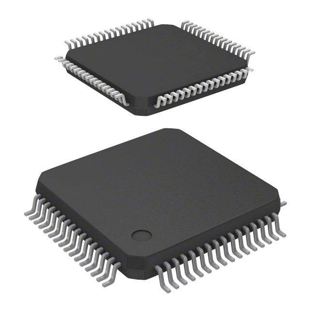
| 供应商器件封装 | 64-LQFP(10x10) |
| 包装 | 托盘 |
| 单位重量 | 346.550 mg |
| 商标 | Freescale Semiconductor |
| 安装类型 | 表面贴装 |
| 安装风格 | SMD/SMT |
| 封装 | Tray |
| 封装/外壳 | 64-LQFP |
| 封装/箱体 | QFP-64 |
| 工作温度 | -40°C ~ 85°C |
| 工作温度范围 | - 40 C to + 85 C |
| 工厂包装数量 | 160 |
| 应用 | Wireless Charging |
| 标准包装 | 160 |
| 电压-电源 | 2.7 V ~ 3.6 V |
| 电流-电源 | - |
| 电源电压 | 3.3 V |
| 类型 | Wireless Charging Controller |
| 输入电压范围 | 3 V to 3.6 V |


- 商务部:美国ITC正式对集成电路等产品启动337调查
- 曝三星4nm工艺存在良率问题 高通将骁龙8 Gen1或转产台积电
- 太阳诱电将投资9.5亿元在常州建新厂生产MLCC 预计2023年完工
- 英特尔发布欧洲新工厂建设计划 深化IDM 2.0 战略
- 台积电先进制程称霸业界 有大客户加持明年业绩稳了
- 达到5530亿美元!SIA预计今年全球半导体销售额将创下新高
- 英特尔拟将自动驾驶子公司Mobileye上市 估值或超500亿美元
- 三星加码芯片和SET,合并消费电子和移动部门,撤换高东真等 CEO
- 三星电子宣布重大人事变动 还合并消费电子和移动部门
- 海关总署:前11个月进口集成电路产品价值2.52万亿元 增长14.8%
PDF Datasheet 数据手册内容提取
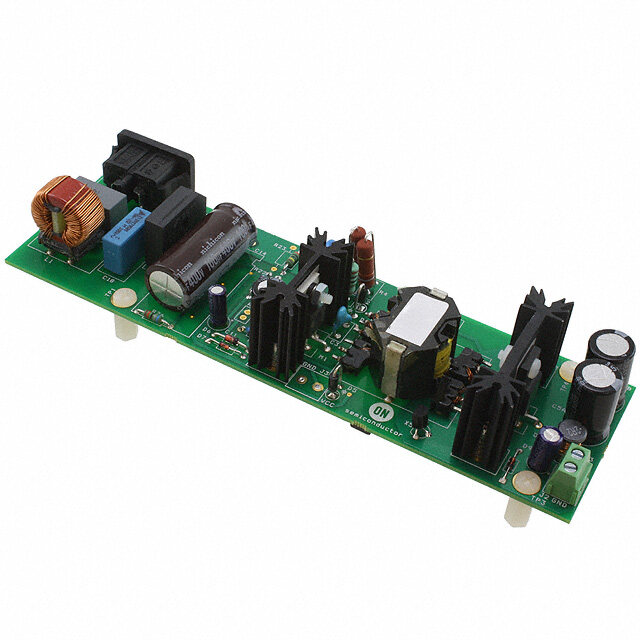
Freescale Semiconductor Document Number: WCT1101DS Data Sheet Rev. 1.0, 02/2014 Consumer Low Power Wireless Transmitter Controller Overview Description The WCT1101 is a wireless power transmitter controller that Features integrates all required functions for WPC “Qi” compliant wireless power transmitter design. It’s an intelligent device Low power (5 W) solution for Wireless Power to work with Freescale touch sensing technology or use Consortium (WPC) compliant transmitter design periodically analog PING (configurable by user) to detect a Conforms to the latest version low power WPC mobile device for charging while gaining super low standby specifications power. Once the mobile device is detected, the WCT1101 Supports wide DC input voltage range starting from controls the power transfer by adjusting the operation 4.2 V, typically 5 V, 12 V and 19 V frequency and duty cycle, or rail voltage, or phase shift of Integrated digital demodulation on chip power stage according to message packets sent by mobile Supports all types of receiver modulation strategies (AC device. capacitor, AC resistor and DC resistor) Supports Foreign Object Detection (FOD) To maximize the design freedom and product differentiation, Super low standby power by Freescale Touch WCT1101 supports any low power consumer power technology transmitter design (WPC A/B types or customization) using Supports any low power consumer power transmitter frequency and duty cycle control, or rail voltage control or solutions using frequency and duty cycle control, or rail phase shift control by software based solution. Besides, voltage control or phase shift control easy-to-use FreeMASTER GUI tool with configuration, calibration and debugging functions provides user-friendly LED & buzzer for system status indication design experience and speed time-to-market. Over-voltage/current/temperature protection Supports CAN/IIC/SCI/SPI interfaces The WCT1101 includes digital demodulation module to Software based solution to provide maximum design reduce external components, over-voltage/current/ freedom and product differentiation temperature protection, FOD method to protect from FreeMASTER GUI tool to enable configuration, overheating by misplaced metallic foreign objects and calibration and debugging general CAN/IIC/SCI/SPI interfaces for external communication purpose. It also handles any abnormal Applications condition and operational status, and provides comprehensive indicator outputs for robust system design. Low Power Wireless Power Transmitter Any lower power consumer power transmitter solution with frequency & duty cycle control, or rail voltage control, or phase-shift control (WPC A/B types or customer properties) Wireless Charging System Functional Diagram © Freescale Semiconductor, Inc., 2014. All rights reserved. _______________________________________________________________________
Contents 1 Absolute Maximum Ratings .................................................................................................................... 4 1.1 Electrical Operating Ratings .................................................................................................................................... 4 1.2 Thermal Handling Ratings ....................................................................................................................................... 5 1.3 ESD Handling Ratings .............................................................................................................................................. 5 1.4 Moisture Handling Ratings ...................................................................................................................................... 5 2 Electrical Characteristics ......................................................................................................................... 5 2.1 General Characteristics ........................................................................................................................................... 5 2.2 Device Characteristics ............................................................................................................................................. 8 2.3 Thermal Operating Characteristics ........................................................................................................................ 17 3 Typical Performance Characteristics ............................................................................................... 18 3.1 System Efficiency .................................................................................................................................................. 18 3.2 Standby Power ...................................................................................................................................................... 18 3.3 Digital Demodulation ............................................................................................................................................ 18 3.4 Foreign Object Detection ...................................................................................................................................... 18 3.5 Dynamic Input Power Limit ................................................................................................................................... 19 4 Device Information ................................................................................................................................. 19 4.1 Functional Block Diagram ...................................................................................................................................... 19 4.2 Product Features Overview ................................................................................................................................... 20 4.3 Pinout Diagram ..................................................................................................................................................... 21 4.4 Pin Function Description ....................................................................................................................................... 22 Consumer Low Power Wireless Transmitter Controller, Rev. 1.0 2 Freescale Semiconductor
4.5 Ordering Information ............................................................................................................................................ 31 4.6 Package Outline Drawing ...................................................................................................................................... 31 5 Software Library ...................................................................................................................................... 31 5.1 Memory Map ........................................................................................................................................................ 32 5.2 Software Library and API Description .................................................................................................................... 32 6 Design Considerations ........................................................................................................................... 32 6.1 Electrical Design Considerations............................................................................................................................ 32 6.2 PCB Layout Considerations .................................................................................................................................... 33 6.3 Thermal Design Considerations ............................................................................................................................. 34 7 References and Links ............................................................................................................................. 34 7.1 References ............................................................................................................................................................ 34 7.2 Useful Links ........................................................................................................................................................... 34 Consumer Low Power Wireless Transmitter Controller, Rev. 1.0 Freescale Semiconductor 3
1 Absolute Maximum Ratings 1.1 Electrical Operating Ratings Table 1. Absolute Maximum Electrical Ratings (V = 0 V, V = 0 V) SS SSA Characteristic Symbol Notes1 Min. Max. Unit Supply Voltage Range V –0.3 4.0 V DD Analog Supply Voltage Range V –0.3 4.0 V DDA ADC High Voltage Reference V –0.3 4.0 V REFHx Voltage difference V to V ΔV –0.3 0.3 V DD DDA DD Voltage difference V to V ΔV –0.3 0.3 V SS SSA ss Digital Input Voltage Range V Pin Group 1 –0.3 5.5 V IN Input Voltage Range V Pin Group 2 –0.3 4.0 V IN_RESET Oscillator Input Voltage Range V Pin Group 4 –0.4 4.0 V OSC Analog Input Voltage Range V Pin Group 3 –0.3 4.0 V INA Input clamp current, per pin (V < V – 0.3 V)2, 3 V – –5.0 mA IN SS IC Output clamp current, per pin4 V – ±20.0 mA OC Contiguous pin DC injection current—regional limit I –25 25 mA Icont sum of 16 contiguous pins Output Voltage Range (normal push-pull mode) V Pin Group 1,2 –0.3 4.0 V OUT Output Voltage Range (open drain mode) V Pin Group 1 –0.3 5.5 V OUTOD Output Voltage Range V Pin Group 2 –0.3 4.0 V OUTOD_RESET DAC Output Voltage Range V Pin Group 5 –0.3 4.0 V OUT_DAC Ambient Temperature T –40 85 °C A Storage Temperature Range T –55 150 °C STG 1. Default Mode: Pin Group 1: GPIO, TDI, TDO, TMS, TCK Pin Group 2: Pin Group 3: ADC and Comparator Analog Inputs Pin Group 4: XTAL, EXTAL Pin Group 5: DAC analog output 2. Continuous clamp current. 3. All 5 volt tolerant digital I/O pins are internally clamped to V through an ESD protection diode. There is no diode connection to V . SS DD If VIN greater than VDIO_MIN (= V –0.3 V) is observed, then there is no need to provide current limiting resistors at the pads. If SS this limit cannot be observed, then a current limiting resistor is required. 4. I/O is configured as push-pull mode. Consumer Low Power Wireless Transmitter Controller, Rev. 1.0 4 Freescale Semiconductor
1.2 Thermal Handling Ratings Table 2. Thermal Handling Ratings Symbol Description Min. Max. Unit Notes T Storage temperature –55 150 °C 1 STG T Solder temperature, lead-free – 260 °C 2 SDR 1. Determined according to JEDEC Standard JESD22-A103, High Temperature Storage Life. 2. Determined according to IPC/JEDEC Standard J-STD-020, Moisture/Reflow Sensitivity Classification for Nonhermetic Solid State Surface Mount Devices. 1.3 ESD Handling Ratings Table 3. ESD Handling Ratings Characteristic1 Min. Max. Unit ESD for Human Body Model (HBM) -2000 +2000 V ESD for Machine Model (MM) -200 +200 V ESD for Charge Device Model (CDM) -500 +500 V Latch-up current at TA= 85°C (I ) -100 +100 mA LAT 1. Parameter is achieved by design characterization on a small sample size from typical devices under typical conditions unless otherwise noted. 1.4 Moisture Handling Ratings Table 4. Moisture Handling Ratings Symbol Description Min. Max. Unit Notes MSL Moisture sensitivity level – 3 – 1 1. Determined according to IPC/JEDEC Standard J-STD-020, Moisture/Reflow Sensitivity Classification for Nonhermetic Solid State Surface Mount Devices. 2 Electrical Characteristics 2.1 General Characteristics Table 5. General Electrical Characteristics Recommended Operating Conditions (V = 0 V, V = 0 V, V = 0 V) REFLx SSA SS Test Characteristic Symbol Notes Min. Typ. Max. Unit Conditions Supply Voltage2 V ,V 2.7 3.3 3.6 V - DD DDA Consumer Low Power Wireless Transmitter Controller, Rev. 1.0 Freescale Semiconductor 5
ADC (Cyclic) Reference VREFHA 3.0 V V - DDA Voltage High V REFHB Voltage difference V to V ΔV -0.1 0 0.1 V - DD DDA DD Voltage difference V to V ΔV -0.1 0 0.1 V - SS SSA ss Input Voltage High (digital V 1 (Pin Group 1) 0.7×V 5.5 V - IH DD inputs) Voltage High V 1 (Pin Group 2) 0.7×V - V V - IH_RESET DD DD Input Voltage Low (digital V 1 (Pin Group 1,2) 0.35×V V - IL DD inputs) Oscillator Input Voltage High XTAL driven by an external VIHOSC 1 (Pin Group 4) 2.0 VDD + 0.3 V - clock source Oscillator Input Voltage Low V 1 (Pin Group 4) -0.3 0.8 V - ILOSC Output Source Current High (at V min.) 3,4 OH • Programmed for low I 1 (Pin Group 1) - -2 - OH drive strength mA 1 (Pin Group 1) - -9 • Programmed for high drive strength Output Source Current Low (at V max.) 3,4 OL • Programmed for low I 1 (Pin Group 1,2) - 2 - OL drive strength mA 1 (Pin Group 1,2) - 9 • Programmed for high drive strength Output Voltage High V 1 (Pin Group 1) V - 0.5 - - V I = I OH DD OH OHmax Output Voltage Low V 1 (Pin Group 1,2) - - 0.5 V I = I OL OL OLmax V = 2.4 V IN 1 (Pin Group 1) Digital Input Current High to 5.5 V I - 0 +/-2.5 µA IH pull-up enabled or disabled VIN = 2.4 V 1 (Pin Group 2) to V DD Comparator Input Current IIHC 1 (Pin Group 3) 0 +/-2 µA VIN = VDDA High Oscillator Input Current High IIHOSC 1 (Pin Group 4) - 0 +/-2 µA VIN = VDDA Internal Pull-Up Resistance R 20 - 50 kΩ - Pull-Up Internal Pull-Down Resistance R 20 - 50 kΩ - Pull-Down Consumer Low Power Wireless Transmitter Controller, Rev. 1.0 6 Freescale Semiconductor
Comparator Input Current IILC 1 (Pin Group 3) - 0 +/-2 µA VIN = 0V Low Oscillator Input Current Low IILOSC 1 (Pin Group 4) - 0 +/-2 µA VIN = 0V R = 3 kΩ, V + V - LD DAC Output Voltage Range VDAC 1 (Pin Group 5) SSA - DDA V CLD = 400 0.04 0.04 pF Output Current1 High I 1 (Pin Group 1,2) - 0 +/-1 µA - OZ Impedance State Schmitt Trigger Input V 1 (Pin Group 1,2) 0.06×V - - V - HYS DD Hysteresis Input capacitance C - 10 - pF - IN Output capacitance C - 10 - pF - OUT GPIO pin interrupt pulse Bus T 6 1.5 - - - width5 INT_Pulse clock Port rise and fall time (high 2.7 ≤ VDD ≤ drive strength). Slew T 7 5.5 - 15.1 ns Port_H_DIS 3.6 V disabled. Port rise and fall time (high 2.7 ≤ VDD ≤ T 7 1.5 - 6.8 ns drive strength). Slew enabled. Port_H_EN 3.6 V Port rise and fall time (low 2.7 ≤ VDD ≤ drive strength). Slew T 8 8.2 - 17.8 ns Port_L_DIS 3.6 V disabled. Port rise and fall time (low 2.7 ≤ VDD ≤ T 8 3.2 - 9.2 ns drive strength). Slew enabled. Port_L_EN 3.6 V Device (system and core) f 0 - 100 MHz - clock frequency SYSCLK Bus clock f - - 50 MHz - BUS 1. Default Mode o Pin Group 1: GPIO, TDI, TDO, TMS, TCK o Pin Group 2: o Pin Group 3: ADC and Comparator Analog Inputs o Pin Group 4: XTAL, EXTAL o Pin Group 5: DAC analog output 2. ADC (Cyclic) specifications are not guaranteed when VDDA is below 3.0 V. 3. Total chip source or sink current cannot exceed 75 mA. 4. Contiguous pin DC injection current of regional limit—including sum of negative injection currents or sum of positive injection currents of 16 contiguous pins—is 25 mA. 5. Applies to a pin only when it is configured as GPIO and configured to cause an interrupt by appropriately programming GPIOn_IPOLR and GPIOn_IENR. 6. The greater synchronous and asynchronous timing must be met. 7. 75 pF load. 8. 15 pF load. Consumer Low Power Wireless Transmitter Controller, Rev. 1.0 Freescale Semiconductor 7
2.2 Device Characteristics Table 6. General Device Characteristics Power mode Transition Behavior Symbol Description Min. Max. Unit Notes After a POR event, the amount of delay from when VDD reaches 2.7 V to when the T 199 225 µs POR first instruction executes (over the operating temperature range). T STOP mode to RUN mode 6.79 7.27 µs 1 S2R T LPS mode to LPRUN mode 240.9 551 µs 2 LPS2LPR T VLPS mode to VLPRUN mode 1424 1459 µs 4 VLPS2VLPR T WAIT mode to RUN mode 0.57 0.62 µs 3 W2R T LPWAIT mode to LPRUN mode 237.2 554 µs 2 LPW2LPR T VLPWAIT mode to VLPRUN mode 1413 1500 µs 4 VLPW2VLPR Power Consumption Operating Behaviors Typical at 3.3 V, 25 °C Mode Conditions Max. Frequency Notes I I DD DDA 100 MHz core clock, 50 MHz peripheral clock, regulators are in full regulation, relaxation oscillator on, PLL powered on, continuous MAC instructions with fetches from program Flash, all peripheral modules enabled, TMRs and SCIs using 1× RUN1 peripheral clock, NanoEdge within 100 MHz 38.1 mA 9.9 mA eFlexPWM using 2× peripheral clock, ADC/DAC (only one 12-bit DAC and all 6-bit DACs) powered on and clocked, comparator powered on, all ports configured as inputs with input low and no DC loads Consumer Low Power Wireless Transmitter Controller, Rev. 1.0 8 Freescale Semiconductor
50 MHz core and peripheral clock, regulators are in full regulation, relaxation oscillator on, PLL powered on, continuous MAC instructions with fetches from program Flash, all peripheral modules enabled, TMRs and SCIs using 1× RUN2 peripheral clock, NanoEdge within 50 MHz 27.6 mA 9.9 mA eFlexPWM using 2× peripheral clock, ADC/DAC (only one 12-bit DAC and all 6-bit DACs) powered on and clocked, comparator powered on, all ports configured as inputs with input low and no DC loads 50 MHz core and peripheral clock, regulators are in full regulation, relaxation oscillator on, PLL powered on, core in WAIT state, all peripheral modules WAIT enabled, TMRs and SCIs using 1× clock, 50 MHz 24.0 mA - NanoEdge within eFlexPWM using 2× clock, ADC/DAC (one 12-bit DAC, all 6-bit DACs)/comparator powered off, all ports configured as inputs with input low and no DC loads 4 MHz core and peripheral clock, regulators are in full regulation, relaxation oscillator on, PLL powered off, core in STOP STOP state, all peripheral module and 4 MHz 6.3 mA - core clocks are off, ADC/DAC/Comparator powered off, all ports configured as inputs with input low and no DC loads 200 kHz core and peripheral clock from relaxation oscillator's low speed clock, relaxation oscillator in standby mode, regulators are in standby, PLL disabled, repeat NOP instructions, all peripheral LPRUN modules enabled, except NanoEdge within 2 MHz 2.8 mA 3.1 mA eFlexPWM and cyclic ADCs, one 12-bit DAC and all 6-bit DACs enabled, simple loop with running from platform instruction buffer, all ports configured as inputs with input low and no DC loads 200 kHz core and peripheral clock from relaxation oscillator's low speed clock, relaxation oscillator in standby mode, regulators are in standby, PLL disabled, all peripheral modules enabled, except LPWAIT 2 MHz 2.7 mA 3.1 mA NanoEdge within eFlexPWM and cyclic ADCs, one 12-bit DAC and all 6-bit DACs enabled, core in WAIT mode, all ports configured as inputs with input low and no DC loads Consumer Low Power Wireless Transmitter Controller, Rev. 1.0 Freescale Semiconductor 9
200 kHz core and peripheral clock from relaxation oscillator's low speed clock, relaxation oscillator in standby mode, regulators are in standby, PLL disabled, LPSTOP only PITs and COP enabled, other 2 MHz 1.2 mA - peripheral modules disabled and clocks gated off, core in STOP mode, all ports configured as inputs with input low and no DC loads 32 kHz core and peripheral clock from a 64 kHz external clock source, oscillator in power down, all relaxation oscillators disabled, large regulator is in standby, small regulator is disabled, PLL disabled, VLPRUN repeat NOP instructions, all peripheral 200 kHz 0.7 mA - modules, except COP and EWM, disabled and clocks gated off, simple loop running from platform instruction buffer, all ports configured as inputs with input low and no DC loads 32 kHz core and peripheral clock from a 64 kHz external clock source, oscillator in power down, all relaxation oscillators disabled, large regulator is in standby, VLPWAIT small regulator is disabled, PLL disabled, 200 kHz 0.7 mA - all peripheral modules, except COP, disabled and clocks gated off, core in WAIT mode, all ports configured as inputs with input low and no DC loads 32 kHz core and peripheral clock from a 64 kHz external clock source, oscillator in power down, all relaxation oscillators disabled, large regulator is in standby, VLPSTOP small regulator is disabled, PLL disabled, 200 kHz 0.7 mA - all peripheral modules, except COP, disabled and clocks gated off, core in STOP mode, all ports configured as inputs with input low and no DC loads Reset and Interrupt Timing Symbol Characteristic Min. Max. Unit Notes t Minimum Assertion Duration 16 - ns 5 RA 865 × T + 8 × OSC t desertion to First Address Fetch - ns 6 RDA T SYSCLK Delay from Interrupt Assertion to Fetch of t 361.3 570.9 ns IF first instruction (exiting STOP mode) PMC Low-Voltage Detection (LVD) and Power-On Reset (POR) Parameters Symbol Characteristic Min. Typ. Max. Unit V POR Assert Voltage7 - 2.0 - V POR_A Consumer Low Power Wireless Transmitter Controller, Rev. 1.0 10 Freescale Semiconductor
V POR Release Voltage8 - 2.7 - V POR_R V LVI_2p7 Threshold Voltage - 2.73 - V LVI_2p7 V LVI_2p2 Threshold Voltage - 2.23 - V LVI_2p2 JTAG Timing Symbol Description Min. Max. Unit Notes fOP TCK frequency of operation DC fSYSCLK/8 MHz tPW TCK clock pulse width 50 - ns tDS TMS, TDI data set-up time 5 - ns tDH TMS, TDI data hold time 5 - ns tDV TCK low to TDO data valid - 30 ns tTS TCK low to TDO tri-state - 30 ns Regulator 1.2 V Parameters Symbol Characteristic Min. Typ. Max. Unit V Output Voltage9 - 1.22 - V CAP I Short Circuit Current10 - 600 - mA SS Short Circuit Tolerance (V shorted to T CAP - - 30 Mins RSC ground) V Reference Voltage (after trim) - 1.21 - V REF External Clock Timing Symbol Characteristic Min. Typ. Max. Unit Frequency of operation (external clock f - - 50 MHz OSC driver) t Clock pulse width11 8 ns PW t External clock input rise time12 - - 1 ns rise t External clock input fall time13 - - 1 ns fall Input high voltage overdrive by an external V 0.85×V - - V ih clock DD Input low voltage overdrive by an external V - - 0.3×V V il clock DD Phase-Locked Loop (PLL) Timing Symbol Characteristic Min. Typ. Max. Unit f PLL input reference frequency14 8 8 16 MHz Ref_PLL f PLL output frequency15 200 - 400 MHz OP_PLL t PLL lock time16 35.5 - 73.2 µs Lock_PLL t Allowed Duty Cycle of input reference 40 50 60 % DC_PLL Consumer Low Power Wireless Transmitter Controller, Rev. 1.0 Freescale Semiconductor 11
External Crystal or Resonator Specifications Symbol Characteristic Min. Typ. Max. Unit f Frequency of operation 4 8 16 MHz XOSC Relaxation Oscillator Electrical Specifications Symbol Characteristic Min. Typ. Max. Unit 8 MHz Output Frequency17 RUN Mode 7.84 8 8.16 MHz • 0 °C to 85 °C f ROSC_8M • -40 °C to 85 °C 7.76 8 8.24 MHz Standby Mode (IRC trimmed @ 8 MHz) • -40 °C to 85 °C - 405 - kHz 8 MHz Frequency Variation over 25 °C RUN Mode f Due to temperature ROSC_8M_Delta • 0 °C to 85 °C - +/-1.5 +/-2 % • -40 °C to 85 °C - +/-1.5 +/-3 % 200 kHz Output Frequency18 f 17 RUN Mode ROSC_200k • -40 °C to 85 °C 194 200 206 kHz 200 kHz Output Frequency Variation over 25 °C18 f RUN Mode ROSC_200k_Delta 17 Due to temperature • 0 °C to 85 °C - +/-1.5 +/-2 % • -40 °C to 85 °C - +/-1.5 +/-3 % Stabilization Time tStab • 8 MHz output19 - 0.12 - µs • 200 kHz output20 - 10 - µs t Output Duty Cycle 48 50 52 % DC_ROSC Flash Specifications Symbol Description Min. Typ. Max. Unit t Longword Program high-voltage time - 7.5 18 µs hvpgm4 t Sector Erase high-voltage time21 - 13 113 ms hversscr t Erase All high-voltage time21 - 52 452 ms hversall Read 1s Section execution time (flash trd1sec1k sector)22 - - 60 µs t Program Check execution time22 - - 45 µs pgmchk t Read Resource execution time22 - - 30 µs rdrsrc t Program Longword execution time - 65 145 µs pgm4 t Erase Flash Sector execution time23 - 14 114 ms ersscr Consumer Low Power Wireless Transmitter Controller, Rev. 1.0 12 Freescale Semiconductor
t Read 1s All Blocks execution time - - 0.9 ms rd1all t Read Once execution time22 - - 25 µs rdonce t Program Once execution time - 65 - µs pgmonce t Erase All Blocks execution time23 - 70 575 ms ersall Verify Backdoor Access Key execution tvfykey time22 - - 30 µs t Data retention after up to 10 K cycles 5 5024 - years flashret10k t Data retention after up to 1 K cycles 20 10024 - years flashret1k n Cycling endurance25 10 K 50 K24 - cycles flashcyc 12-bit Cyclic ADC Electrical Specifications Symbol Characteristic Min. Typ. Max. Unit V Supply voltage26 3.0 3.3 3.6 V DDA V V supply voltage27 V - 0.6 V V REFHX REFH DDA DDA f ADC conversion clock28 0.1 - 10 MHz ADCCLK Conversion range29 V - R • Fully differential -( V - V ) - REFH V ADC REFH REFL V REFL • Single-ended/unipolar V - V REFL V REFH Input voltage range (per input)30 VADCIN • External Reference VREFL - VREFH V • Internal Reference VSSA - VDDA V t Conversion time - 8 - t ADC ADCCLK t ADC power-up time (from adc_pdn) - 13 - t ADCPU ADCCLK I ADC RUN current (per ADC block) - 1.8 - mA ADCRUN ADC power down current (adc_pdn I - 0.1 - µA ADPWRDWN enabled) I V current (in external mode) - 190 225 µA VREFH REFH INL Integral non-linearity31 - +/- 1.5 +/- 2.2 LSB32 ADC DNL Differential non-linearity31 - +/- 0.5 +/- 0.8 LSB32 ADC Offset33 V • Fully differential - +/- 8 - mV OFFSET • Single ended/Unipolar - +/- 12 - mV 0.99 to E Gain Error - 0.996 to 1.004 - GAIN 1.101 ENOB Effective number of bits - 10.6 - bits I Input injection current34 - - +/-3 mA INJ CADCI Input sampling capacitance - 4.8 - pF 12-bit DAC Electrical Specifications Symbol Characteristic Min. Typ. Max. Unit Consumer Low Power Wireless Transmitter Controller, Rev. 1.0 Freescale Semiconductor 13
Settling time35 under R = 3 kΩ, C = 400 t LD LD - 1 - µs SETTLE pF DAC power-up time (from PWRDWN t - - 11 µs DACPU release to valid DACOUT) INL Integral non-linearity37 - +/- 3 +/- 4 LSB36 DAC DNL Differential non-linearity37 - +/- 0.8 +/- 0.9 LSB36 DAC Monotonicity (> 6 sigma monotonicity, < MON Guaranteed - DAC 3.4 ppm non-monotonicity) V Offset error37 (5% to 95% of full range) - +/- 25 +/- 43 mV OFFSET E Gain error37 (5% to 95% of full range) - +/- 0.5 +/- 1.5 % GAIN V Output voltage range V + 0.04 - V - 0.04 V OUT SSA DDA SNR Signal-to-noise ratio - 85 - dB ENOB Effective number of bits - 11 - bits Comparator and 6-bit DAC Electrical Specifications Symbol Description Min. Typ. Max. Unit V Supply voltage 2.7 - 3.6 V DD Supply current, High-speed mode(EN=1, I - 300 - µA DDHS PMODE=1) Supply current, Low-speed mode(EN=1, I - 36 - µA DDLS PMODE=0) V Analog input voltage V - V V AIN ss DD V Analog input offset voltage - - 20 mV AIO Analog comparator hysteresis38 - 5 13 mV • CR0[HYSTCTR]=00 - 25 48 mV V • CR0[HYSTCTR]=01 H - 55 105 mV • CR0[HYSTCTR]=10 • CR0[HYSTCTR]=11 - 80 148 mV V Output high V - 0.5 - - V CMPOh DD V Output low - - 0.5 V CMPOl Propagation delay, high-speed t - 25 50 ns DHS mode(EN=1, PMODE=1)39 Propagation delay, low-speed t - 60 200 ns DLS mode(EN=1, PMODE=0) 39 t Analog comparator initialization delay40 - 40 - µs DInit I 6-bit DAC current adder (enabled) - 7 - µA DAC6b R 6-bit DAC reference inputs V - V V DAC6b DDA DD Consumer Low Power Wireless Transmitter Controller, Rev. 1.0 14 Freescale Semiconductor
INL 6-bit DAC integral non-linearity -0.5 - 0.5 LSB41 DAC6b DNL 6-bit DAC differential non-linearity -0.3 - 0.3 LSB41 DAC6b eFlexPWM Timing Parameters Symbol Characteristic Min. Typ. Max. Unit f PWM clock frequency - 100 - MHz PWM S NanoEdge Placement (NEP) step size42,43 - 312 - ps PWMNEP Delay for fault input activating to PWM t 1 - - ns DFLT output deactivated t Power-up time44 - 25 - µs PWMPU Quad Timer Timing Symbol Characteristic Min. Max. Unit Notes P Timer input period 2T + 6 - ns 45 IN timer P Timer input high/low period 1T + 3 - ns 45 INHL timer P Timer output period 2T - 2 - ns 45 OUT timer P Timer output high/low period 1T - 2 - ns 45 OUTHL timer QSPI Timing Min. Max. Symbol Characteristic Unit Master Slave Master Slave t Cycle time 60 60 - - ns C t Enable lead time - 20 - - ns ELD t Enable lag time - 20 - - ns ELG t Clock (SCLK) high time 28 28 - - ns CH t Clock (SCLK) low time 28 28 - - ns CL t Data set-up time required for inputs 20 1 - - ns DS t Data hold time required for inputs 1 3 - - ns DH Access time (time to data active from t 5 - ns A high-impedance state) Disable time (hold time to high-impedance t 5 - ns D state) t Data valid for outputs - - ns DV t Data invalid 0 0 - - ns DI t Rise time - - 1 1 ns R t Fall time - - 1 1 ns F QSCI Timing Symbol Characteristic Min. Max. Unit Notes BR Baud rate - (f /16) Mbit/s 46 SCI MAX_SCI PW RXD pulse width 0.965/BR 1.04/BR ns RXD SCI SCI Consumer Low Power Wireless Transmitter Controller, Rev. 1.0 Freescale Semiconductor 15
PW TXD pulse width 0.965/BR 1.04/BR ns TXD SCI SCI CAN Timing Symbol Characteristic Min. Max. Unit Notes BR Baud rate - 1 Mbit/s CAN T CAN Wakeup dominant pulse filtered - 1.5 µs WAKEUP T CAN Wakeup dominant pulse pass 5 - µs WAKEUP IIC Timing Min. Max. Symbol Characteristic Unit Notes Min. Max. Min. Max. fSCL SCL clock frequency 0 100 0 400 kHz Hold time (repeated) START condition. t After this period, the first clock pulse is 4 - 0.6 - µs HD_STA generated. t LOW period of the SCL clock 4.7 - 1.3 - µs SCL_LOW t HIGH period of the SCL clock 4 - 0.6 - µs SCL_HIGH Set-up time for a repeated START t 4.7 - 0.6 - µs SU_STA condition t Data hold time for IIC bus devices 047 3.4548 049 0.947 µs HD_DAT t Data set-up time 25050 - 10051 - ns 48 SU_DAT t Rise time of SDA and SCL signals - 1000 20 + 0.1C 300 ns 52 r b t Fall time of SDA and SCL signals - 300 20 + 0.1C 300 ns 51 f b tSU_STOP Set-up time for STOP condition 4 - 0.6 - µs Bus free time between STOP and START t 4.7 - 1.3 - µs BUS_Free condition Pulse width of spikes that must be tSP suppressed by the input filter N/A N/A 0 50 ns 1. CPU clock = 4 MHz and System running from 8 MHz IRC Applicable to all wakeup times: Wakeup times (in 1,2,3,4) are measured from GPIO toggle for wakeup till GPIO toggle at the wakeup interrupt subroutine from respective stop/wait mode. 2. CPU clock = 200 kHz and 8 MHz IRC on standby. Exit via interrupt on Port C GPIO. 3. Clock configuration: CPU and system clocks= 100 MHz; Bus Clock = 50 MHz. Exit via an interrupt on PortC GPIO. 4. Using 64 KHz external clock; CPU Clock = 32 KHz. Exit via an interrupt on PortC GPIO. 5. If the pin filter is enabled by setting the RST_FLT bit in the SIM_CTRL register to 1, the minimum pulse assertion must be greater than 21 ns. 6. TOSC means oscillator clock cycle; TSYSCLK means system clock cycle. 7. During 3.3 V VDD power supply ramp down. 8. During 3.3 V VDD power supply ramp up (gated by LVI_2p7). 9. Value is after trim. 10. Guaranteed by design. 11. The chip may not function if the high or low pulse width is smaller than 6.25 ns. 12. External clock input rise time is measured from 10% to 90%. 13. External clock input fall time is measured from 90% to 10%. 14. An externally supplied reference clock should be as free as possible from any phase jitter for the PLL to work correctly. The PLL is optimized for 8 MHz input. 15. The frequency of the core system clock cannot exceed 100 MHz. If the NanoEdge PWM is available, the PLL output must be set to 400 MHz. Consumer Low Power Wireless Transmitter Controller, Rev. 1.0 16 Freescale Semiconductor
16. This is the time required after the PLL is enabled to ensure reliable operation. 17. Frequency after application of 8 MHz trimmed. 18. Frequency after application of 200 kHz trimmed. 19. Standby to run mode transition. 20. Power down to run mode transition. 21. Maximum time based on expectations at cycling end-of-life. 22. Assumes 25 MHz flash clock frequency. 23. Maximum times for erase parameters based on expectations at cycling end-of-life. 24. Typical data retention values are based on measured response accelerated at high temperature and derated to a constant 25°C use profile. Engineering Bulletin EB618 does not apply to this technology. Typical endurance defined in Engineering Bulletin EB619. 25. Cycling endurance represents number of program/erase cycles at -40°C ≤ Tj ≤ 125°C. 26. The ADC functions up to VDDA = 2.7 V. When VDDA is below 3.0 V, ADC specifications are not guaranteed. 27. When the input is at the V level, the resulting output will be all zeros (hex 000), plus any error contribution due to offset and gain REFL error. When the input is at the V level the output will be all ones (hex FFF), minus any error contribution due to offset and gain REFH error. 28. ADC clock duty cycle is 45% ~ 55%. 29. Conversion range is defined for x1 gain setting. For x2 and x4 the range is 1/2 and 1/4, respectively. 30. In unipolar mode, positive input must be ensured to be always greater than negative input. 31. INL /DNL is measured from VADCIN = VREFL to VADCIN = VREFH using Histogram method at x1 gain setting. ADC ADC 32. Least Significant Bit = 0.806 mV at 3.3 V VDDA, x1 gain setting. 33. Any off-channel with 50 kHz full-scale input to the channel being sampled with DC input (isolation crosstalk). 34. The current that can be injected into or sourced from an unselected ADC input without affecting the performance of the ADC. 35. Settling time is swing range from VSSA to VDDA. 36. LSB = 0.806 mV. 37. No guaranteed specification within 5% of VDDA or VSSA. 38. Typical hysteresis is measured with input voltage range limited to 0.7 to VDD-0.7 V. 39. Signal swing is 100 mV. 40. Comparator initialization delay is defined as the time between software writes to change control inputs (Writes to DACEN, VRSEL, PSEL, MSEL, VOSEL) and the comparator output settling to a stable level. 41. 1 LSB = Vreference/64. 42. Reference IPbus clock of 100 MHz in NanoEdge Placement mode. 43. Temperature and voltage variations do not affect NanoEdge Placement step size. 44. Powerdown to NanoEdge mode transition. 45. Ttimer = Timer input clock cycle. For 100 MHz operation, Ttimer = 10 ns. 46. fMAX_SCI is the frequency of operation of the SCI clock in MHz, which can be selected as the bus clock or 2x bus clock for the device. 47. The master mode IIC deasserts ACK of an address byte simultaneously with the falling edge of SCL. If no slaves acknowledge this address byte, then a negative hold time can result, depending on the edge rates of the SDA and SCL lines. 48. The maximum tHD_DAT must be met only if the device does not stretch the LOW period (tSCL_LOW) of the SCL signal. 49. Input signal Slew = 10 ns and Output Load = 50 pF 50. Set-up time in slave-transmitter mode is 1 IPBus clock period, if the TX FIFO is empty. 51. A Fast mode IIC bus device can be used in a Standard mode IIC bus system, but the requirement tSU_DAT ≥ 250 ns must then be met. This is automatically the case if the device does not stretch the LOW period of the SCL signal. If such a device does stretch the LOW period of the SCL signal, then it must output the next data bit to the SDA line trmax + tSU_DAT = 1000 + 250 = 1250 ns (according to the Standard mode IIC bus specification) before the SCL line is released. 52. Cb = total capacitance of the one bus line in pF. 2.3 Thermal Operating Characteristics Table 7. General Thermal Characteristics Symbol Description Min. Max. Unit T Die junction temperature -40 125 °C J T Ambient temperature -40 85 °C A Consumer Low Power Wireless Transmitter Controller, Rev. 1.0 Freescale Semiconductor 17
3 Typical Performance Characteristics 3.1 System Efficiency The typical maximum system efficiency (receiver output power vs. transmitter input power) on Freescale WCT1101 based transmitter solutions can usually reach 70 plus percentage. Of course, the detailed number depends on the specific solution type. For example, Freescale A11 reference solution has more than 75% system efficiency with bq51013AEVM-764 receiver module. Note: Power components are the main factor to determine the system efficiency, such as drivers and MOSFETs. 3.2 Standby Power The purpose of the standby mode of operation is to reduce the power consumption of a wireless power transfer system when power transfer is not required. There are two ways to enter standby mode. The first is when the transmitter doesn’t detect the presence of a valid receiver. The second is when the receiver sends only an End Power Transfer Packet. In standby mode, the transmitter only monitors if a receiver is placed on the active charging area of the transmitter or removed there from. It is recommended that the transmitter’s power consumption in standby mode meets the relative regional regulations especially for “No-load power consumption”. In Freescale A11 reference design solution: Transmitter power consumption in standby mode with Analog PING technology: < 12 mA (60 mW with 5 V DC input) Transmitter power consumption in standby mode with Touch Sensor technology: < 5 mA (25 mW with 5 V DC input) 3.3 Digital Demodulation To optimize system BOM cost, WCT1101 solution employs digital demodulation algorithm to communicate with receiver. This method can achieve high performance, low cost, and very simple coil signal sensing circuit with less component number. 3.4 Foreign Object Detection WCT1101 solution employs flexible, intelligent and easy-to-use FOD algorithm to ensure accurate foreign metal objects detection. With Freescale FreeMASTER GUI tool, FOD algorithm can be easily calibrated to get accurate power loss information especially for very sensitive foreign objects. Consumer Low Power Wireless Transmitter Controller, Rev. 1.0 18 Freescale Semiconductor
3.5 Dynamic Input Power Limit When the transmitter is powered by a limited power supply, such as USB power, WCT1101 can limit the transmitter output power and provide necessary margin relative to the input power supply capability. By monitoring the input voltage and input current of the transmitter, when it drops to a specified level and still positive Control Error Packet (CEP) is received, WCT1101 will stop increasing power output and control transmitter operation in input power limit status. Users can know the system is in DIPL control mode by LED indication, LED1 and LED2 will be in fast blinking mode when input power is limited. WCT1101 will exit DIPL control mode and return to normal PID control mode if a negative Control Error Packet (CEP) is received to reduce output power. The input voltage level for DIPL control can be configured in the WCT1101 example project. 4 Device Information 4.1 Functional Block Diagram This functional block diagram just shows the functional block pin assignment information of MWCT1101CLH. For the detailed pin multiplexing information, please see Section 4.4 of “Pin Function Description”. Consumer Low Power Wireless Transmitter Controller, Rev. 1.0 Freescale Semiconductor 19
Figure 3. MWCT1101CLH Function Block Diagram 4.2 Product Features Overview The following table highlights the main on-chip resource features of MWCT1101 device. Table 8. Product Features Overview Part WCT1101 Maximum Core/Bus Clock (MHz) 100/50 Maximum Fully Run Current Consumption (mA) 38.1 (V ) + 9.9 (V ) DD DDA On-Chip Program Flash Memory Size (KB) 64 On-Chip SRAM Memory Size (KB) 8 Memory Resource Protection Yes Inter-Peripheral Crossbar Switches with AOI Yes On-Chip Relaxation Oscillator 1 (8 MHz) + 1 (200 kHz) Windowed Computer Operating Properly 1 External Watchdog Monitor 1 Cyclic Redundancy Check 1 Consumer Low Power Wireless Transmitter Controller, Rev. 1.0 20 Freescale Semiconductor
Periodic Interrupt Timer 2 Quad Timer 1 x 4 12-bit Cyclic ADC Channels 2 x 8 High-Resolution 8 PWM Channels Standard 4 12-bit DAC 2 Analog Comparator /w 6-bit REF DAC 4 DMA Channels 4 Queued Serial Communications Interface 2 Queued Serial Peripheral Interface 2 Inter-Integrated Circuit 1 Controller Area Network (MSCAN) 1 GPIO 54 Package 64 LQFP 4.3 Pinout Diagram Figure 4. MWCT1101CLH Pinout Diagram Consumer Low Power Wireless Transmitter Controller, Rev. 1.0 Freescale Semiconductor 21
4.4 Pin Function Description By default, each pin is configured for its primary function (listed first). Any alternative functionality, shown in parentheses, can be programmed through GPIO module peripheral enable registers and SIM module GPIO peripheral select registers. Table 9. Pin Signal Descriptions Multiplexing Signal Name Pin No. Function Description Signals Test Clock Input — This input pin provides a gated clock to synchronize the test logic and shift serial data to the JTAG/EOnCE port. The pin is connected internally to a pull-up resistor. A Schmitt-trigger input is used for noise immunity. TCK 1 GPIOD2 Port D GPIO — This GPIO pin can be individually programmed as an input or output pin. After reset, the default state is TCK. — This input is a direct hardware reset on the processor. When is asserted low, the device is initialized and placed in the reset state. A Schmitt-trigger input is used for noise immunity. The internal reset signal is de-asserted synchronous with the internal clocks after a fixed number of internal clocks. 2 GPIOD4 Port D GPIO — This GPIO pin can be individually programmed as an input or output pin. If functionality is disabled in this mode and the chip can be reset only via POR, COP reset, or software reset. After reset, the default state is . Port C GPIO — This GPIO pin can be individually programmed as an input or output pin. EXTAL — External Crystal Oscillator Input. This input connects the internal GPIOC0 3 EXTAL/CLKIN0 crystal oscillator input to an external crystal or ceramic resonator. CLKIN0 — This pin serves as an external clock input 0. After reset, the default state is GPIOC0. Port C GPIO — This GPIO pin can be individually programmed as an input or output pin. GPIOC1 4 XTAL XTAL — External Crystal Oscillator Output. This output connects the internal crystal oscillator output to an external crystal or ceramic resonator. After reset, the default state is GPIOC1. Port C GPIO — This GPIO pin can be individually programmed as an input or output pin. TXD0 — The SCI0 transmit data output or transmit/receive in single wire operation. TXD0/XB_OUT GPIOC2 5 11/XB_IN2/CLK XB_OUT11 — Crossbar module output 11. O0 XB_IN2 — Crossbar module input 2. CLKO0 — This is a buffered clock output 0; the clock source is selected by clock out select (CLKOSEL) bits in the clock output select register (CLKOUT) of the SIM. Consumer Low Power Wireless Transmitter Controller, Rev. 1.0 22 Freescale Semiconductor
After reset, the default state is GPIOC2. Port F GPIO — This GPIO pin can be individually programmed as an input or output pin. RXD0 — The SCI0 receive data input. RXD0/XB_OUT XB_OUT10 — Crossbar module output 10. GPIOF8 6 10/CMPD_O/P WM_2X CMPD_O — Analog comparator D output. PWM_2X — NanoEdge eFlexPWM sub-module 2 output X or input capture X. After reset, the default state is GPIOF8. Port C GPIO — This GPIO pin can be individually programmed as an input or output pin. TA0 — Quad timer module A channel 0 input/output. TA0/CMPA_O/ CMPA_O — Analog comparator A output. GPIOC3 7 RXD0/CLKIN1 RXD0 — The SCI0 receive data input. CLKIN1 — This pin serves as an external clock input 1. After reset, the default state is GPIOC3. Port C GPIO — This GPIO pin can be individually programmed as an input or output pin. TA1 — Quad timer module A channel 1 input/output. TA1/CMPB_O/X CMPB_O — Analog comparator B output. GPIOC4 8 B_IN6/ XB_IN6 — Crossbar module input 6. — External watchdog monitor output. After reset, the default state is GPIOC4. Port A GPIO — This GPIO pin can be individually programmed as an input or output pin. ANA7&CMPD_I ANA7&CMPD_IN3 — Analog input to channel 7 of ADCA and input 3 of GPIOA7 9 N3 analog comparator D. When used as an analog input, the signal goes to the ANA7 and CMPD_IN3. After reset, the default state is GPIOA7. Port A GPIO — This GPIO pin can be individually programmed as an input or output pin. ANA6&CMPD_I ANA6&CMPD_IN2 — Analog input to channel 6 of ADCA and input 2 of GPIOA6 10 N2 analog comparator D. When used as an analog input, the signal goes to the ANA6 and CMPD_IN2. After reset, the default state is GPIOA6. Port A GPIO — This GPIO pin can be individually programmed as an input or output pin. ANA5&CMPD_I GPIOA5 11 N1 ANA5&CMPD_IN1 — Analog input to channel 5 of ADCA and input 1 of analog comparator D. When used as an analog input, the signal goes to the Consumer Low Power Wireless Transmitter Controller, Rev. 1.0 Freescale Semiconductor 23
ANA5 and CMPD_IN1. After reset, the default state is GPIOA5. Port A GPIO — This GPIO pin can be individually programmed as an input or output pin. ANA4&CMPD_I ANA4&CMPD_IN0 — Analog input to channel 4 of ADCA and input 0 of GPIOA4 12 N0 analog comparator D. When used as an analog input, the signal goes to the ANA4 and CMPD_IN0. After reset, the default state is GPIOA4. Port A GPIO — This GPIO pin can be individually programmed as an input or output pin. ANA0&CMPA_IN3 — Analog input to channel 0 of ADCA and input 3 of ANA0&CMPA_I analog comparator A. When used as an analog input, the signal goes to the GPIOA0 13 N3/CMPC_O ANA0 and CMPA_IN3. CMPC_O — Analog comparator C output. After reset, the default state is GPIOA0. Port A GPIO — This GPIO pin can be individually programmed as an input or output pin. ANA1&CMPA_I ANA1 and CMPA_IN0 — Analog input to channel 1 of ADCA and input 0 of GPIOA1 14 N0 analog comparator A. When used as an analog input, the signal goes to the ANA1 and CMPA_IN0. After reset, the default state is GPIOA1. Port A GPIO — This GPIO pin can be individually programmed as an input or output pin. ANA2&VREFHA&CMPA_IN1 — Analog input to channel 2 of ADCA and ANA2&VREFH GPIOA2 15 analog references high of ADCA and input 1 of analog comparator A. When A&CMPA_IN1 used as an analog input, the signal goes to ANA2 and VREFHA and CMPA_IN1. ADC control register configures this input as ANA2 or VREFHA. After reset, the default state is GPIOA2. Port A GPIO — This GPIO pin can be individually programmed as an input or output pin. ANA3&VREFLA&CMPA_IN2 — Analog input to channel 3 of ADCA and ANA3&VREFLA GPIOA3 16 analog references low of ADCA and input 2 of analog comparator A. When &CMPA_IN2 used as an analog input, the signal goes to ANA3 and VREFLA and CMPA_IN2. ADC control register configures this input as ANA3 or VREFLA. After reset, the default state is GPIOA3. Port B GPIO — This GPIO pin can be individually programmed as an input or output pin. ANB7&CMPB_I ANB7&CMPB_IN2 — Analog input to channel 7 of ADCB and input 2 of GPIOB7 17 N2 analog comparator B. When used as an analog input, the signal goes to the ANB7 and CMPB_IN2. After reset, the default state is GPIOB7. Port C GPIO — This GPIO pin can be individually programmed as an input or output pin. DACA_O/XB_IN GPIOC5 18 7 DACA_O — 12-bit Digital-to-Analog Converter A output. Consumer Low Power Wireless Transmitter Controller, Rev. 1.0 24 Freescale Semiconductor
XB_IN7 — Crossbar module input 7. After reset, the default state is GPIOC5. Port B GPIO — This GPIO pin can be individually programmed as an input or output pin. ANB6&CMPB_I ANB6&CMPB_IN1 — Analog input to channel 6 of ADCB and input 1 of GPIOB6 19 N1 analog comparator B. When used as an analog input, the signal goes to the ANB6 and CMPB_IN1. After reset, the default state is GPIOB6. Port B GPIO — This GPIO pin can be individually programmed as an input or output pin. ANB5&CMPC_I ANB5&CMPC_IN2 — Analog input to channel 5 of ADCB and input 2 of GPIOB5 20 N2 analog comparator C. When used as an analog input, the signal goes to the ANB5 and CMPC_IN2. After reset, the default state is GPIOB5. Port B GPIO — This GPIO pin can be individually programmed as an input or output pin. ANB4&CMPC_I ANB4&CMPC_IN1 — Analog input to channel 4 of ADCB and input 1 of GPIOB4 21 N1 analog comparator C. When used as an analog input, the signal goes to the ANB4 and CMPC_IN1. After reset, the default state is GPIOB4. Analog Power — This pin supplies 3.3 V power to the analog modules. It VDDA 22 - must be connected to a clean analog power supply. Analog Ground — This pin supplies an analog ground to the analog VSSA 23 - modules. It must be connected to a clean power supply. Port B GPIO — This GPIO pin can be individually programmed as an input or output pin. ANB0&CMPB_I ANB0&CMPB_IN3 — Analog input to channel 0 of ADCB and input 3 of GPIOB0 24 N3 analog comparator B. When used as an analog input, the signal goes to ANB0 and CMPB_IN3. After reset, the default state is GPIOB0. Port B GPIO — This GPIO pin can be individually programmed as an input or output pin. ANB1&CMPB_IN0 — Analog input to channel 1 of ADCB and input 0 of ANB1&CMPB_I analog comparator B. When used as an analog input, the signal goes to GPIOB1 25 N0/DACB_O ANB1 and CMPB_IN0. DACB_O — 12-bit Digital-to-Analog Converter B output. After reset, the default state is GPIOB1. Connect a 2.2 μF or greater bypass capacitor between this pin and VSS to VCAP1 26 - stabilize the core voltage regulator output required for proper device operation. Port B GPIO — This GPIO pin can be individually programmed as an input or output pin. ANB2&VREFH ANB2&VREFHB&CMPC_IN3 — Analog input to channel 2 of ADCB and GPIOB2 27 B&CMPC_IN3 analog references high of ADCB and input 3 of analog comparator C. When used as an analog input, the signal goes to ANB2 and VREFHB and CMPC_IN3. ADC control register configures this input as ANB2 or VREFHB. Consumer Low Power Wireless Transmitter Controller, Rev. 1.0 Freescale Semiconductor 25
After reset, the default state is GPIOB2. Port B GPIO — This GPIO pin can be individually programmed as an input or output pin. ANB3&VREFLB&CMPC_IN0 — Analog input to channel 3 of ADCB and ANB3&VREFLB GPIOB3 28 analog references low of ADCB and input 0 of analog comparator C. When &CMPC_IN0 used as an analog input, the signal goes to ANB3 and VREFLB and CMPC_IN0. ADC control register configures this input as ANB3 or VREFLB. After reset, the default state is GPIOB3. VDD1 29 - I/O Power — Supplies 3.3 V power to on-chip digital module. VSS1 30 - I/O Ground — Provides ground on-chip digital module. Port C GPIO — This GPIO pin can be individually programmed as an input or output pin. TA2 — Quad timer module A channel 2 input/output. XB_IN3 — Crossbar module input 3. TA2/XB_IN3/C GPIOC6 31 MP_REF/ CMP_REF — Input 5 of analog comparator A and B and C and D. — is used in slave mode to indicate to the SPI0 module that the current transfer is to be received. After reset, the default state is GPIOC6. Port C GPIO — This GPIO pin can be individually programmed as an input or output pin. — is used in slave mode to indicate to the SPI0 module that the current transfer is to be received. /TXD0/XB_I GPIOC7 32 N8 TXD0 — SCI0 transmit data output or transmit/receive in single wire operation. XB_IN8 — Crossbar module input 8. After reset, the default state is GPIOC7. Port C GPIO — This GPIO pin can be individually programmed as an input or output pin. MISO0 — Master in/slave out. In master mode, this pin serves as the data input. In slave mode, this pin serves as the data output. The MISO0 line of a slave device is placed in the high-impedance state if the slave device is not MISO0 selected. GPIOC8 33 /RXD0/XB_IN9/ XB_OUT6 RXD0 — SCI0 receive data input. XB_IN9 — Crossbar module input 9. XB_OUT6 — Crossbar module output 6. After reset, the default state is GPIOC8. Port C GPIO — This GPIO pin can be individually programmed as an input or output pin. SCLK0/XB_IN4/ GPIOC9 34 TXD0/XB_OUT SCLK0 — The SPI0 serial clock. In master mode, this pin serves as an 8 output, clocking slaved listeners. In slave mode, this pin serves as the data clock input. Consumer Low Power Wireless Transmitter Controller, Rev. 1.0 26 Freescale Semiconductor
XB_IN4 — Crossbar module input 4. TXD0 — SCI0 transmit data output or transmit/receive in single wire operation. XB_OUT8 — Crossbar module output 8. After reset, the default state is GPIOC9. Port C GPIO — This GPIO pin can be individually programmed as an input or output pin. MOSI0 — Master out/slave in. In master mode, this pin serves as the data output. In slave mode, this pin serves as the data input. XB_IN5 — Crossbar module input 5. MOSI0 GPIOC10 35 /XB_IN5/MISO0 MISO0 — Master in/slave out. In master mode, this pin serves as the data /XB_OUT9 input. In slave mode, this pin serves as the data output. The MISO0 line of a slave device is placed in the high-impedance state if the slave device is not selected. XB_OUT9 — Crossbar module output 9. After reset, the default state is GPIOC10. Port F GPIO — This GPIO pin can be individually programmed as an input or output pin. XB_IN6 — Crossbar module input 6. GPIOF0 36 XB_IN6/SCLK1 SCLK1 — The SPI1 serial clock. In master mode, this pin serves as an output, clocking slaved listeners. In slave mode, this pin serves as the data clock input. After reset, the default state is GPIOF0. Port C GPIO — This GPIO pin can be individually programmed as an input or output pin. CANTX — CAN transmit data output. CAN_TX/SCL0/ GPIOC11 37 SCL0 — IIC0 serial clock. TXD1 TXD1 — SCI1 transmit data output or transmit/receive in single wire operation. After reset, the default state is GPIOC11. Port C GPIO — This GPIO pin can be individually programmed as an input or output pin. CANRX — CAN receive data input. CAN_RX/SDA0/ GPIOC12 38 RXD1 SDA0 — IIC0 serial data line. RXD1 — SCI1 receive data input. After reset, the default state is GPIOC12. Port F GPIO — This GPIO pin can be individually programmed as an input or output pin. SCL0/XB_OUT GPIOF2 39 6/MISO1 SCL0 — IIC0 serial clock. XB_OUT6 — Crossbar module output 6. Consumer Low Power Wireless Transmitter Controller, Rev. 1.0 Freescale Semiconductor 27
MISO1 — Master in/slave out. In master mode, this pin serves as the data input. In slave mode, this pin serves as the data output. The MISO1 line of a slave device is placed in the high-impedance state if the slave device is not selected. After reset, the default state is GPIOF2. Port F GPIO — This GPIO pin can be individually programmed as an input or output pin. SDA0 — IIC0 serial data line. SDA0/XB_OUT GPIOF3 40 XB_OUT7 — Crossbar module output 7. 7/ MOSI1 MOSI1 — Master out/slave in. In master mode, this pin serves as the data output. In slave mode, this pin serves as the data input. After reset, the default state is GPIOF3. Port F GPIO — This GPIO pin can be individually programmed as an input or output pin. TXD1 — The SCI1 transmit data output or transmit/receive in single wire operation. TXD1/XB_OUT XB_OUT8 — Crossbar module output 8. GPIOF4 41 8/PWM_0X/PW M_FAULT6 PWM_0X — NanoEdge eFlexPWM sub-module 0 output X or input capture X. PWM_FAULT6 — NanoEdge eFlexPWM fault input 6. After reset, the default state is GPIOF4. Port F GPIO — This GPIO pin can be individually programmed as an input or output pin. RXD1 — The SCI1 receive data input. RXD1/XB_OUT XB_OUT9 — Crossbar module output 9. GPIOF5 42 9/PWM_1X/PW M_FAULT7 PWM_1X — NanoEdge eFlexPWM sub-module 1 output X or input capture X. PWM_FAULT7 — NanoEdge eFlexPWM fault input 7. After reset, the default state is GPIOF5. VSS2 43 - I/O Ground — Provides ground to on-chip digital module. VDD2 44 - I/O Power — Supplies 3.3 V power to on-chip digital module. Port E GPIO — This GPIO pin can be individually programmed as an input or output pin. GPIOE0 45 PWM_0B PWM_0B — NanoEdge eFlexPWM sub-module 0 output B or input capture B. After reset, the default state is GPIOE0. Port E GPIO — This GPIO pin can be individually programmed as an input or output pin. GPIOE1 46 PWM_0A PWM_0A — NanoEdge eFlexPWM sub-module 0 output A or input capture A. Consumer Low Power Wireless Transmitter Controller, Rev. 1.0 28 Freescale Semiconductor
After reset, the default state is GPIOE1. Port E GPIO — This GPIO pin can be individually programmed as an input or output pin. GPIOE2 47 PWM_1B PWM_1B — NanoEdge eFlexPWM sub-module 1 output B or input capture B. After reset, the default state is GPIOE2. Port E GPIO — This GPIO pin can be individually programmed as an input or output pin. GPIOE3 48 PWM_1A PWM_1A — NanoEdge eFlexPWM sub-module 1 output A or input capture A. After reset, the default state is GPIOE3. Port C GPIO — This GPIO pin can be individually programmed as an input or output pin. TA3 — Quad timer module A channel 3 input/output. TA3/XB_IN6/ GPIOC13 49 XB_IN6 — Crossbar module input 6. — External watchdog monitor output. After reset, the default state is GPIOC13. Port F GPIO — This GPIO pin can be individually programmed as an input or output pin. CLKO1 — This is a buffered clock output 1; the clock source is selected by clock out select (CLKOSEL) bits in the clock output select register CLKO1/XB_IN7/ (CLKOUT) of the SIM. GPIOF1 50 CMPD_O XB_IN7 — Crossbar module input 7. CMPD_O — Analog comparator D output. After reset, the default state is GPIOF1. Port E GPIO — This GPIO pin can be individually programmed as an input or output pin. PWM_2B — NanoEdge eFlexPWM sub-module 2 output B or input capture PWM_2B/XB_I GPIOE4 51 B. N2 XB_IN2 — Crossbar module input 2. After reset, the default state is GPIOE4. Port E GPIO — This GPIO pin can be individually programmed as an input or output pin. PWM_2A — NanoEdge eFlexPWM sub-module 2 output A or input capture PWM_2A/XB_I GPIOE5 52 A. N3 XB_IN3 — Crossbar module input 3. After reset, the default state is GPIOE5. Port E GPIO — This GPIO pin can be individually programmed as an input or output pin. PWM_3B/XB_I GPIOE6 53 N4 PWM_3B — NanoEdge eFlexPWM sub-module 3 output B or input capture B. Consumer Low Power Wireless Transmitter Controller, Rev. 1.0 Freescale Semiconductor 29
XB_IN4 — Crossbar module input 4. After reset, the default state is GPIOE6. Port E GPIO — This GPIO pin can be individually programmed as an input or output pin. PWM_3A — NanoEdge eFlexPWM sub-module 3 output A or input capture PWM_3A/XB_I GPIOE7 54 A. N5 XB_IN5 — Crossbar module input 5. After reset, the default state is GPIOE7. Port C GPIO — This GPIO pin can be individually programmed as an input or output pin. SDA0 — IIC0 serial data line. SDA0/XB_OUT GPIOC14 55 4/PWM_FAULT XB_OUT4 — Crossbar module output 4. 4 PWM_FAULT4 — NanoEdge eFlexPWM fault input 4. After reset, the default state is GPIOC14. Port C GPIO — This GPIO pin can be individually programmed as an input or output pin. SCL0 — IIC0 serial clock. SCL0/XB_OUT GPIOC15 56 5/PWM_FAULT XB_OUT5 — Crossbar module output 5. 5 PWM_FAULT5 — NanoEdge eFlexPWM fault input 5. After reset, the default state is GPIOC15. Connect a 2.2 μF or greater bypass capacitor between this pin and VSS to VCAP2 57 - stabilize the core voltage regulator output required for proper device operation. Port F GPIO — This GPIO pin can be individually programmed as an input or output pin. PWM_3X — NanoEdge eFlexPWM sub-module 3 output X or input capture PWM_3X/XB_I GPIOF6 58 X. N2 XB_IN2 — Crossbar module input 2. After reset, the default state is GPIOF6. Port F GPIO — This GPIO pin can be individually programmed as an input or output pin. CMPC_O— Analog comparator C output. CMPC_O/ /X GPIOF7 59 — is used in slave mode to indicate to the SPI1 module that the B_IN3 current transfer is to be received. XB_IN3 — Crossbar module input 3. After reset, the default state is GPIOF7. VDD3 60 - I/O Power — Supplies 3.3 V power to on-chip digital module. VSS3 61 - I/O Ground — Provides ground to on-chip digital module. Test Data Output — This tri-stateable output pin provides a serial output TDO 62 GPIOD1 data stream from the JTAG/EOnCE port. It is driven in the shift-IR and Consumer Low Power Wireless Transmitter Controller, Rev. 1.0 30 Freescale Semiconductor
shift-DR controller states, and changes on the falling edge of TCK. Port D GPIO — This GPIO pin can be individually programmed as an input or output pin. After reset, the default state is TDO. Test Mode Select Input — This input pin is used to sequence the JTAG TAP controller’s state machine. It is sampled on the rising edge of TCK and has an on-chip pull-up resistor. Port D GPIO — This GPIO pin can be individually programmed as an input TMS 63 GPIOD3 or output pin. After reset, the default state is TMS. NOTE: Always tie the TMS pin to VDD through a 2.2 kΩ resistor if need to keep on-board debug capability. Otherwise, directly tie to VDD. Test Data Input — This input pin provides a serial input data stream to the JTAG/EOnCE port. It is sampled on the rising edge of TCK and has an on-chip pull-up resistor. TDI 64 GPIOD0 Port D GPIO — This GPIO pin can be individually programmed as an input or output pin. After reset, the default state is TDI. 4.5 Ordering Information Table 1 lists the pertinent information needed to place an order. Consult a Freescale Semiconductor sales office to determine availability and to order this device. Table 10 MWCT1101CLH Ordering Information Device Supply Voltage Package Type Pin Count Ambient Temp. Order Number MWCT1101CLH 3.0 to 3.6V LQFP 64 -40 to +85℃ MWCT1101CLH 4.6 Package Outline Drawing To find a package drawing, go to freescale.com and perform a keyword search for the drawing’s document number of 98ASS23234W. 5 Software Library WCT1101 can not only run the core wireless charging function, but also allow user to add user application functions. Freescale provides two Wireless Charging Transmitter (WCT) software libraries (WCT1000 TX library and WCT1200 TX library) for different solutions design on WCT1101. In these libraries, low level drivers of HAL (Hardware Abstract Layer), callback functions for library access are open to user. For the software API and library details, see WCT1000 TX Library User Guide.pdf (WCT1000LIBUG). Consumer Low Power Wireless Transmitter Controller, Rev. 1.0 Freescale Semiconductor 31
5.1 Memory Map WCT1101 has large on-chip Flash memory and RAM for user design. Besides for wireless charging transmitter library code, the user can develop private functions and link it to library through predefined APIs. Table 11. WCT1101 Memory Footprint Part Memory Total Size Library Size FreeMASTER Size EEPROM Size Free Size Flash 64 Kbytes 19 Kbytes 1.5 Kbytes 1 Kbytes 42.5 Kbytes WCT1101 RAM 8 Kbytes 5.8 Kbytes 0.1 Kbytes 0 Kbytes 2.1 Kbytes 5.2 Software Library and API Description For more and detailed information about WCT software library and API definition, see WCT1000 TX Library User Guide.pdf (WCT1000LIBUG). 6 Design Considerations 6.1 Electrical Design Considerations Use the following list of considerations to assure correct operation of the device and system: The minimum bypass requirement is to place 0.01 - 0.1μF capacitors positioned as near as possible to the package supply pins. The recommended bypass configuration is to place one bypass capacitor on each of the VDD/VSS pairs, including VDDA/VSSA. Ceramic and tantalum capacitors tend to provide better tolerances. Bypass the VDD and VSS with approximately 10μF, plus the number of 0.1μF ceramic capacitors. Consider all device loads as well as parasitic capacitance due to PCB traces when calculating capacitance. This is especially critical in systems with higher capacitive loads that could create higher transient currents in the VDD and VSS circuits. Take special care to minimize noise levels on the VDDA, and VSSA pins. Using separate power planes for VDD and VDDA and separate ground planes for VSS and VSSA are recommended. Connect the separate analog and digital power and ground planes as near as possible to power supply outputs. If an analog circuit and digital circuit are powered by the same power supply, you should connect a small inductor or ferrite bead in serial with VDDA trace. If desired, connect an external RC circuit to the RESET pin. The resistor value should be in the range of 4.7 kΩ – 10 kΩ; and the capacitor value should be in the range of 0.1μF – 4.7μF. Consumer Low Power Wireless Transmitter Controller, Rev. 1.0 32 Freescale Semiconductor
Add a 2.2 kΩ external pull-up on the TMS pin of the JTAG port to keep device in a restate during normal operation if JTAG converter is not present. During reset and after reset but before I/O initialization, all I/O pins are at input mode with internal weak pull-up. To eliminate PCB trace impedance effect, each ADC input should have a no less than 33pF/10 Ω RC filter. To assure chip reliable operation, please reserve enough margin for chip electrical design. The figure 6 shows the relationship between electrical ratings and electrical operating characteristics for correct chip operation. Electrical rating (min.) Electrical operating characteristics (minE.l)ectrical operating characteristics (maxE.l)ectrical rating (max.) Fatal range Degraded operating range Normal operating range Degraded operating range Fatal range Expected permanent failure - No permanent failure - No permanent failure - No permanent failure Expected permanent failure - Possible decreased life - Correct operation - Possible decreased life - Possible incorrect operation - Possible incorrect operation Operating (power on) Handling rating (min.) Handling rating (max.) Fatal range Handling range Fatal range Expected permanent failure No permanent failure Expected permanent failure Handling (power off) Figure 6. Relationship between Ratings and Operating Characteristics 6.2 PCB Layout Considerations Provide a low-impedance path from the board power supply to each VDD pin on the device and from the board ground to each VSS pin. Ensure that capacitor leads and associated printed circuit traces that connect to the chip VDD and VSS pins are as short as possible. PCB trace lengths should be minimal for high-frequency signals. Physically separate analog components from noisy digital components by ground planes. Do not place an analog trace in parallel with digital traces. Place an analog ground trace around an analog signal trace to isolate it from digital traces. The decoupling capacitors of 0.1μF must be placed on the VDD pins as close as possible, and place those ceramic capacitors on the same PCB layer with WCT1101 device. VIA is not recommend between the VDD pins and decoupling capacitors. Consumer Low Power Wireless Transmitter Controller, Rev. 1.0 Freescale Semiconductor 33
The WCT1101 bottom EP pad should be soldered to the ground plane, which will make the system more stable, and VIA matrix method can be used to connect this pad to the ground plane. As the Wireless Charging system functions as a switching-mode power supply, the power components layout is very important for the whole system power transfer efficiency and EMI performance. The power routing loop should be small and short as can as possible, especially for the resonant network, the traces of this circuit should be short and wide, and the current loop should be optimized smaller for the MOSFETs, resonant capacitor and primary coil. Another important thing is that the control circuit and power circuit should be separated. 6.3 Thermal Design Considerations WCT1101 power consumption is not so critical, so there is not additional part needed for power dissipation. However, the power inverter needs the additional PCB Cu copper to dissipate the heat, so good thermal package MOSFET is recommended to select, such as DFN package, and for the resonant capacitor, COG material, and 1206 or 1210 package are recommended to meet the thermal requirement. And the worst thermal case is on the inverter, so the user should make some special actions to dissipate the heat for good transmitter system thermal performance. 7 References and Links 7.1 References WCT1000 A11 Reference Design System User Guide (WCT1000SYSUG) WCT1000 TX Library User Guide (WCT1000LIBUG) WCT Runtime Debug User Guide (WCT1XXXRTDUG) WCT1000 A11 Reference Design Calibration User Guide (WCT1000CALUG) WPC Low Power Wireless Transfer System Description Part 1: Interface Definition Version 1.1 7.2 Useful Links freescale.com freescale.com\wirelesscharging www.wirelesspowerconsortium.com Consumer Low Power Wireless Transmitter Controller, Rev. 1.0 34 Freescale Semiconductor
How to Reach Us: Information in this document is provided solely to enable system and software implementers to use Freescale products. There are no express or implied copyright Home Page: licenses granted hereunder to design or fabricate any integrated circuits based on the freescale.com information in this document. Web Support: Freescale reserves the right to make changes without further notice to any products herein. freescale.com/support Freescale makes no warranty, representation, or guarantee regarding the suitability of its products for any particular purpose, nor does Freescale assume any liability arising out of the application or use of any product or circuit, and specifically disclaims any and all liability, including without limitation consequential or incidental damages. “Typical” parameters that may be provided in Freescale data sheets and/or specifications can and do vary in different applications, and actual performance may vary over time. All operating parameters, including “typicals,” must be validated for each customer application by customer’s technical experts. Freescale does not convey any license under its patent rights nor the rights of others. Freescale sells products pursuant to standard terms and conditions of sale, which can be found at the following address: freescale.com/SalesTermsandConditions. Freescale and the Freescale logo are trademarks of Freescale Semiconductor, Inc., Reg. U.S. Pat. & Tm. Off. All other product or service names are the property of their respective owners. ©2014 Freescale Semiconductor, Inc. Document Number: WCT1101DS Rev. 1.0 02/2014
Mouser Electronics Authorized Distributor Click to View Pricing, Inventory, Delivery & Lifecycle Information: N XP: MWCT1000CFM MWCT1101CLH