ICGOO在线商城 > 射频/IF 和 RFID > RF 放大器 > MW7IC915NT1
 Datasheet下载
- 型号: MW7IC915NT1
- 制造商: Freescale Semiconductor
- 库位|库存: xxxx|xxxx
- 要求:
| 数量阶梯 | 香港交货 | 国内含税 |
| +xxxx | $xxxx | ¥xxxx |
查看当月历史价格
查看今年历史价格
MW7IC915NT1产品简介:
ICGOO电子元器件商城为您提供MW7IC915NT1由Freescale Semiconductor设计生产,在icgoo商城现货销售,并且可以通过原厂、代理商等渠道进行代购。 MW7IC915NT1价格参考¥226.46-¥231.65。Freescale SemiconductorMW7IC915NT1封装/规格:RF 放大器, 射频放大器 IC W-CDMA 728MHz ~ 960MHz 24-PQFN(8x8)。您可以下载MW7IC915NT1参考资料、Datasheet数据手册功能说明书,资料中有MW7IC915NT1 详细功能的应用电路图电压和使用方法及教程。
| 参数 | 数值 |
| 产品目录 | |
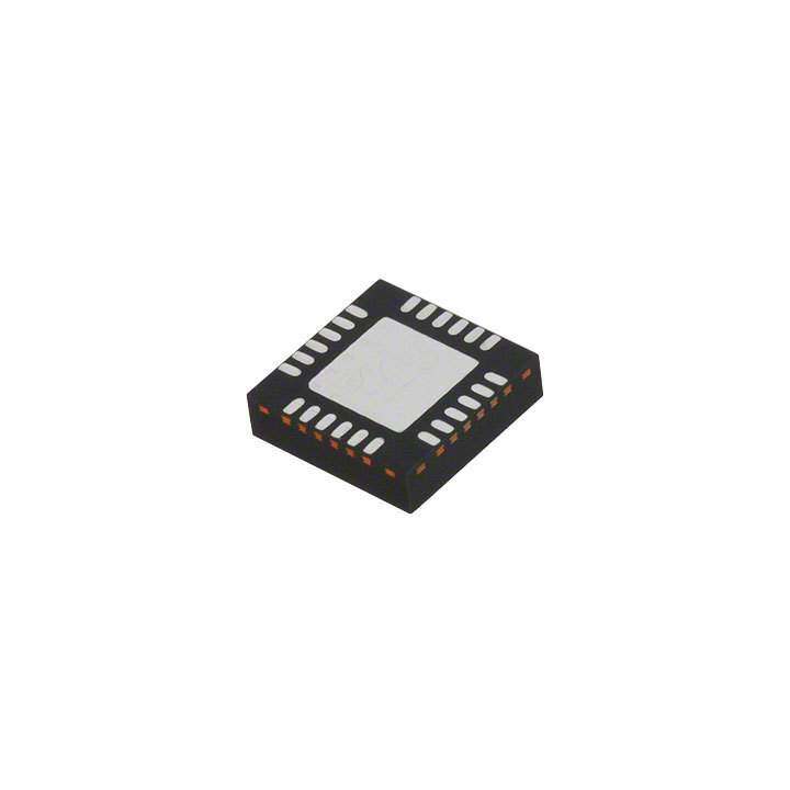
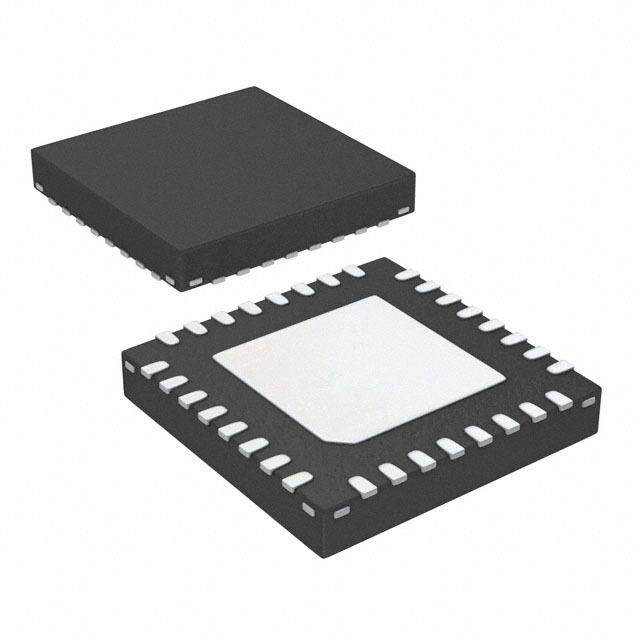
| 描述 | IC PWR AMP HV7 900MHZ 15W 24PQFN |
| 产品分类 | |
| 品牌 | Freescale Semiconductor |
| 数据手册 | |
| 产品图片 |
|
| P1dB | 15.5W |
| 产品型号 | MW7IC915NT1 |
| RF类型 | W-CDMA |
| rohs | 无铅 / 符合限制有害物质指令(RoHS)规范要求 |
| 产品系列 | - |
| 供应商器件封装 | 24-PQFN(8x8) |
| 其它名称 | MW7IC915NT1DKR |
| 包装 | Digi-Reel® |
| 噪声系数 | - |
| 增益 | 38dB |
| 封装/外壳 | 24-PowerQFN |
| 标准包装 | 1 |
| 测试频率 | - |
| 电压-电源 | 28V |
| 电流-电源 | - |
| 频率 | 728MHz ~ 960MHz |


- 商务部:美国ITC正式对集成电路等产品启动337调查
- 曝三星4nm工艺存在良率问题 高通将骁龙8 Gen1或转产台积电
- 太阳诱电将投资9.5亿元在常州建新厂生产MLCC 预计2023年完工
- 英特尔发布欧洲新工厂建设计划 深化IDM 2.0 战略
- 台积电先进制程称霸业界 有大客户加持明年业绩稳了
- 达到5530亿美元!SIA预计今年全球半导体销售额将创下新高
- 英特尔拟将自动驾驶子公司Mobileye上市 估值或超500亿美元
- 三星加码芯片和SET,合并消费电子和移动部门,撤换高东真等 CEO
- 三星电子宣布重大人事变动 还合并消费电子和移动部门
- 海关总署:前11个月进口集成电路产品价值2.52万亿元 增长14.8%


PDF Datasheet 数据手册内容提取
Freescale Semiconductor DocumentNumber:MW7IC915N Technical Data Rev.2,12/2013 RF LDMOS Wideband Integrated Power Amplifier MW7IC915NT1 The MW7IC915N wideband integrated circuit is designed with on--chip matching that makes it usable from 698 to 960 MHz. This multi--stage structureisratedfor26to32voltoperationandcoversalltypicalcellularbase stationmodulationformats. DriverApplication—900MHz TypicalSingle--CarrierW--CDMAPerformance:VDD=28Volts, 728--960MHz,1.6WAVG.,28V I =52mA,I =134mA,P =1.6WattsAvg.,IQMagnitude SINGLEW--CDMA DQ1 DQ2 out Clipping,ChannelBandwidth=3.84MHz,InputSignalPAR=7.5dB RFLDMOSWIDEBAND @0.01%ProbabilityonCCDF. INTEGRATEDPOWERAMPLIFIER Gps PAE ACPR Frequency (dB) (%) (dBc) 865MHz 37.9 17.1 --50.4 880MHz 38.0 17.4 --50.6 895MHz 37.8 17.5 --51.3 CapableofHandling10:1VSWR,@32Vdc,880MHz,Pout=23.5WattsCW (3dBInputOverdrivefromRatedPout) PQFN88 PLASTIC Stableintoa5:1VSWR.AllSpursBelow--60dBc@30to41.5dBmCW P . out TypicalPout@1dBCompressionPoint≃15.5WattsCW DriverApplication—700MHz TypicalSingle--CarrierW--CDMAPerformance:VDD=28Volts, I =50mA,I =144mA,P =1.6WattsAvg.,IQMagnitude DQ1 DQ2 out Clipping,ChannelBandwidth=3.84MHz,InputSignalPAR=7.5dB @0.01%ProbabilityonCCDF. Gps PAE ACPR Frequency (dB) (%) (dBc) 728MHz 37.8 17.2 --49.5 748MHz 37.8 17.3 --50.5 768MHz 37.7 17.3 --51.4 Features CharacterizedwithSeriesEquivalentLarge--SignalImpedanceParameters andCommonSourceS--Parameters On--ChipMatching(50OhmInput,DCBlocked) IntegratedQuiescentCurrentTemperatureCompensationwith Enable/DisableFunction(1) IntegratedESDProtection InTapeandReel.T1Suffix=1,000Units,16mmTapeWidth,13--inchReel. 1. RefertoAN1977,QuiescentCurrentThermalTrackingCircuitintheRFIntegratedCircuitFamilyandtoAN1987,QuiescentCurrentControl fortheRFIntegratedCircuitDeviceFamily.Gotohttp://www.freescale.com/rf.SelectDocumentation/ApplicationNotes--AN1977orAN1987. FreescaleSemiconductor,Inc.,2009,2013.Allrightsreserved. MW7IC915NT1 RFDeviceData FreescaleSemiconductor,Inc. 1
VGS1 VGS2 1 2 GS C GSC C C V N V N N N QuiescentCurrent 24 23 22 21 20 19 TemperatureCompensation(1) NC 1 18 RFout/VDS2 GND 2 17 RFout/VDS2 RFin 3 16 RFout/VDS2 RFin 4 15 RFout/VDS2 RFin RFout/VDS2 GND 5 14 RFout/VDS2 NC 6 7 8 9 10 11 12 13 RFout/VDS2 NC DS1 DS1NC NC NC VDS1 V V Figure1.FunctionalBlockDiagram Figure2.PinConnections 1. RefertoAN1977,QuiescentCurrentThermalTrackingCircuitintheRFIntegratedCircuitFamilyandtoAN1987,QuiescentCurrentControl fortheRFIntegratedCircuitDeviceFamily.Gotohttp://www.freescale.com/rf.SelectDocumentation/ApplicationNotes--AN1977orAN1987. Table1.MaximumRatings Rating Symbol Value Unit Drain--SourceVoltage VDSS --0.5,+65 Vdc Gate--SourceVoltage VGS --6.0,+10 Vdc OperatingVoltage VDD 32,+0 Vdc StorageTemperatureRange Tstg --65to+150 C OperatingJunctionTemperature(1) TJ 150 C InputPower Pin 17 dBm Table2.ThermalCharacteristics Characteristic Symbol Value(1,2) Unit ThermalResistance,JunctiontoCase RJC C/W W--CDMAApplication Stage1,28Vdc,IDQ1=60mA 7.5 (CaseTemperature82C,Pout=1.6WCW) Stage2,28Vdc,IDQ2=130mA 3.2 Table3.ESDProtectionCharacteristics TestMethodology Class HumanBodyModel(perJESD22--A114) 1B MachineModel(perEIA/JESD22--A115) A ChargeDeviceModel(perJESD22--C101) III Table4.MoistureSensitivityLevel TestMethodology Rating PackagePeakTemperature Unit PerJESD22--A113,IPC/JEDECJ--STD--020 3 260 C 1. MTTFcalculatoravailableathttp://www.freescale.com/rf.SelectSoftware&Tools/DevelopmentTools/CalculatorstoaccessMTTF calculatorsbyproduct. 2. RefertoAN1955,ThermalMeasurementMethodologyofRFPowerAmplifiers.Gotohttp://www.freescale.com/rf. SelectDocumentation/ApplicationNotes--AN1955. MW7IC915NT1 RFDeviceData 2 FreescaleSemiconductor,Inc.
Table5.ElectricalCharacteristics (TA=25Cunlessotherwisenoted) Characteristic Symbol Min Typ Max Unit Stage1—OffCharacteristics ZeroGateVoltageDrainLeakageCurrent IDSS — — 10 Adc (VDS=65Vdc,VGS=0Vdc) ZeroGateVoltageDrainLeakageCurrent IDSS — — 1 Adc (VDS=28Vdc,VGS=0Vdc) Gate--SourceLeakageCurrent IGSS — — 1 Adc (VGS=1.5Vdc,VDS=0Vdc) Stage1—OnCharacteristics GateThresholdVoltage VGS(th) 1 2 3 Vdc (VDS=10Vdc,ID=9Adc) GateQuiescentVoltage VGS(Q) — 3 — Vdc (VDS=28Vdc,ID=52mAdc) FixtureGateQuiescentVoltage VGG(Q) 5.5 6.3 7 Vdc (VDD=28Vdc,ID=52mAdc,MeasuredinFunctionalTest) Stage2—OffCharacteristics ZeroGateVoltageDrainLeakageCurrent IDSS — — 10 Adc (VDS=65Vdc,VGS=0Vdc) ZeroGateVoltageDrainLeakageCurrent IDSS — — 1 Adc (VDS=28Vdc,VGS=0Vdc) Gate--SourceLeakageCurrent IGSS — — 1 Adc (VGS=1.5Vdc,VDS=0Vdc) Stage2—OnCharacteristics GateThresholdVoltage VGS(th) 1 2 3 Vdc (VDS=10Vdc,ID=36Adc) GateQuiescentVoltage VGS(Q) — 2.9 — Vdc (VDS=28Vdc,ID=134mAdc) FixtureGateQuiescentVoltage VGG(Q) 3.8 4.6 5.3 Vdc (VDD=28Vdc,ID=134mAdc,MeasuredinFunctionalTest) Drain--SourceOn--Voltage VDS(on) 0.1 0.3 0.8 Vdc (VGS=10Vdc,ID=3.6Adc) FunctionalTests(1)(InFreescaleTestFixture,50ohmsystem)VDD=28Vdc,IDQ1=52mA,IDQ2=134mA,Pout=1.6WAvg., f=880MHz,Single--CarrierW--CDMA,IQMagnitudeClipping,InputSignalPAR=7.5dB@0.01%ProbabilityonCCDF.ACPRmeasured in3.84MHzChannelBandwidth@5MHzOffset. PowerGain Gps 35.0 38.0 41.0 dB PowerAddedEfficiency PAE 15.0 17.4 — % AdjacentChannelPowerRatio ACPR — --50.6 --47.0 dBc InputReturnLoss IRL — --22 --9 dB TypicalPerformanceoverFrequency(InFreescaleTestFixture,50ohmsystem)VDD=28Vdc,IDQ1=52mA,IDQ2=134mA,Pout=1.6W Avg.,Single--CarrierW--CDMA,IQMagnitudeClipping,InputSignalPAR=7.5dB@0.01%ProbabilityonCCDF.ACPRmeasuredin 3.84MHzChannelBandwidth@5MHzOffset. Gps PAE ACPR IRL Frequency (dB) (%) (dBc) (dB) 865MHz 37.9 17.1 --50.4 --21 880MHz 38.0 17.4 --50.6 --22 895MHz 37.8 17.5 --51.3 --22 1. Partinternallyinputmatched. (continued) MW7IC915NT1 RFDeviceData FreescaleSemiconductor,Inc. 3
Table5.ElectricalCharacteristics(TA=25Cunlessotherwisenoted)(continued) Characteristic Symbol Min Typ Max Unit TypicalPerformances(InFreescaleTestFixture,50ohmsystem)VDD=28Vdc,IDQ1=52mA,IDQ2=134mA,865--895MHzBandwidth Pout@1dBCompressionPoint,CW P1dB — 15.5 — W (VDD=28Vdc,IDQ1=75mA,IDQ2=100mA) IMDSymmetry@16WPEP,PoutwhereIMDThirdOrder IMDsym MHz Intermodulation30dBc — 45 — (DeltaIMDThirdOrderIntermodulationbetweenUpperandLower Sidebands>2dB) VBWResonancePoint VBWres — 180 — MHz (IMDThirdOrderIntermodulationInflectionPoint) QuiescentCurrentAccuracyoverTemperature(1) Stage1 IQT — 0.10 — % with2kGateFeedResistors(--30to85C) Stage2 — 0.12 — GainFlatnessin30MHzBandwidth@Pout=1.6WAvg. GF — 0.1 — dB GainVariationoverTemperature G — 0.041 — dB/C (--30Cto+85C) OutputPowerVariationoverTemperature P1dB — 0.004 — dBm/C (--30Cto+85C) TypicalPerformance—700MHz(InFreescale700MHzTestFixture,50ohmsystem)VDD=28Vdc,IDQ1=50mA,IDQ2=144mA,Pout= 1.6WAvg.,Single--CarrierW--CDMA,IQMagnitudeClipping,InputSignalPAR=7.5dB@0.01%ProbabilityonCCDF.ACPRmeasuredin 3.84MHzChannelBandwidth@5MHzOffset. Gps PAE ACPR IRL Frequency (dB) (%) (dBc) (dB) 728MHz 37.8 17.2 --49.5 --23 748MHz 37.8 17.3 --50.5 --22 768MHz 37.7 17.3 --51.4 --22 1. RefertoAN1977,QuiescentCurrentThermalTrackingCircuitintheRFIntegratedCircuitFamilyandtoAN1987,QuiescentCurrentControl fortheRFIntegratedCircuitDeviceFamily.Gotohttp://www.freescale.com/rf.SelectDocumentation/ApplicationNotes -- AN1977or AN1987. MW7IC915NT1 RFDeviceData 4 FreescaleSemiconductor,Inc.
VG1 VG2 C8 C10 C12 C19 R1 R2 C13 C15 C17 VD2 C7 C9 C11 C1 C2 C3 C4 C5 C6 C14 MW7IC915N Rev3 C16 C18 VD1 C20 Figure3.MW7IC915NT1TestCircuitComponentLayout Table6.MW7IC915NT1TestCircuitComponentDesignationsandValues Part Description PartNumber Manufacturer C1 1.8pFChipCapacitor ATC100B1R8BT500XT ATC C2,C5 0.8pFChipCapacitors ATC100B0R8BT500XT ATC C3 6.2pFChipCapacitor ATC100B6R2BT500XT ATC C4 3.3pFChipCapacitor ATC100B3R3CT500XT ATC C6,C11,C12,C13,C14 47pFChipCapacitors ATC100B470JT500XT ATC C7,C8 1FChipCapacitors GRM31MR71H105KA88L Murata C9,C10 0.1FChipCapacitors GRM32MR71H104JA01L Murata C15,C16 4.7FChipCapacitors GRM31CR71H475KA12L Murata C17,C18 10F,50VChipCapacitors GRM55DR61H106KA88L Murata C19,C20 100F,50VElectrolyticCapacitors MCGPR50V107M8X11--RH Multicomp R1,R2 2k,1/4WResistors CRCW12062K00FKEA Vishay PCB 0.020,r=3.66 RO4350B Rogers MW7IC915NT1 RFDeviceData FreescaleSemiconductor,Inc. 5
TYPICALCHARACTERISTICS 40 19 D PAE DE%) 39 18 D( AY Gps ERNC 38 17 WE B) OCI GAIN(d 37 VIDDQD2==21834VdmcA,,PSouintg=le1--.6CaWrri(eArvWg.-)-,CIDDQM1A=,532.8m4AMHz 16 PAE,PEFFI B) R 36 ChannelBandwidth,InputSignalPAR=7.5dB@ --46 (d E S G,POWps 333354 0.01%ProbabilityonCCDF IRL PARC ------444789 ACPR(dBc) ------312000 TRETURNLOS 00--0.5.5 ARC(dB) U P ACPR P N 32 --50 --40 I --1 L, 800 820 840 860 880 900 920 940 960 980 1000 R I f,FREQUENCY(MHz) Figure4.OutputPeak--to--AverageRatioCompression(PARC) BroadbandPerformance@P =1.6WattsAvg. out --5 Bc) --10 VDD=28Vdc,Pout=16W(PEP),IDQ1=52mA N(d --15 IDQ2=134mA,Two--ToneMeasurements O (f1+f2)/2=CenterFrequencyof880MHz TI --20 R TO --25 IM3--U DIS --30 IM3--L N --35 O IM5--U TI --40 A UL --45 IM5--L OD --50 IM7--U M ER --55 IM7--L NT --60 I D, --65 M I --70 1 10 100 200 TWO--TONESPACING(MHz) Figure5.IntermodulationDistortionProducts versusTwo--ToneSpacing 40 1 60 --20 VDD=28Vdc,IDQ1=52mA,IDQ2=134mA,f=880MHz Single--CarrierW--CDMA,3.84MHzChannelBandwidth %) 39.5 % 0 50 ( --25 OWERGAIN(dB) 383.59 MPRESSIONAT0.01LITYONCCDF(dB) ----12 PAGRCpsPAE --1dB=3.8W --3d--B2=dB6.=95W.2W 4300 ADDEDEFFICIENCY ----3305 ACPR(dBc) G,Pps 38 UTCOOBABI --3 20 OWER --40 PR P 37.5 UTP --4 ACPR InputSignalPAR=7.5dB@0.01% 10 E, --45 O ProbabilityonCCDF PA 37 --5 0 --50 2 4 6 8 10 Pout,OUTPUTPOWER(WATTS) Figure6.OutputPeak--to--AverageRatio Compression(PARC)versusOutputPower MW7IC915NT1 RFDeviceData 6 FreescaleSemiconductor,Inc.
TYPICALCHARACTERISTICS 41 90 --15 VDD=28Vdc,IDQ1=52mA,IDQ2=134mA,Single--Carrier 40 W--CDMA,3.84MHzChannelBandwidth,InputSignal 80 %) --20 PAR=7.5dB@0.01%ProbabilityonCCDF ( Y 39 70 C --25 (dB) 895MHz CIEN GAIN 38 Gps 895MHz 880MHz 865MHz 60 EFFI --30 Bc) R 37 50 D --35 d E E ( W D R G,POps 3365 895MH8z80MHz 865MHz 880MHz 4300 OWERAD ----4405 ACP ACPR P 34 20 AE, --50 PAE P 33 10 --55 1 10 20 Pout,OUTPUTPOWER(WATTS)AVG. Figure7.Single--CarrierW--CDMAPowerGain,PowerAdded EfficiencyandACPRversusOutputPower 40 0 Gain 30 --5 20 --10 AIN(dB) 10 --15 RL(dB) G I 0 VDD=28Vdc --20 Pin=--30dBm IRL --10 IDQ1=52mA --25 IDQ2=134mA --20 --30 300 600 900 1200 f,FREQUENCY(MHz) Figure8.BroadbandFrequencyResponse W--CDMATESTSIGNAL 100 10 0 10 --10 3.84MHz %) 1 --20 ChannelBW ( Y InputSignal --30 T BILI 0.1 --40 BA B) O d R 0.01 ( --50 P W--CDMA.ACPRMeasuredin3.84MHz --60 --ACPRin3.84MHz +ACPRin3.84MHz 0.001 ChannelBandwidth@5MHzOffset. IntegratedBW IntegratedBW InputSignalPAR=7.5dB@0.01% --70 ProbabilityonCCDF 0.0001 --80 0 1 2 3 4 5 6 7 8 9 10 --90 PEAK--TO--AVERAGE(dB) --100 Figure9.CCDFW--CDMAIQMagnitude --9 --7.2 --5.4 --3.6 --1.8 0 1.8 3.6 5.4 7.2 9 Clipping,Single--CarrierTestSignal f,FREQUENCY(MHz) Figure10.Single--CarrierW--CDMASpectrum MW7IC915NT1 RFDeviceData FreescaleSemiconductor,Inc. 7
VDD=28Vdc,IDQ1=52mA,IDQ2=134mA,Pout=1.6WAvg. f Zin Zload MHz 820 52.99--j29.47 7.72+j13.96 840 49.35--j27.56 7.34+j14.74 860 46.67--j23.60 7.43+j15.55 880 44.88--j17.63 7.94+j16.07 900 43.73--j10.46 7.98+j16.74 920 43.12--j2.75 7.80+j17.62 940 43.38+j5.01 8.28+j18.33 960 44.07+j12.97 9.07+j19.04 980 43.89+j12.61 9.14+j20.02 Zin = Deviceinputimpedanceasmeasuredfrom gatetoground. Zload = Testcircuitimpedanceasmeasuredfrom draintoground. Device Output UnderTest Matching Network Z Z in load Figure11.SeriesEquivalentInputandLoadImpedance MW7IC915NT1 RFDeviceData 8 FreescaleSemiconductor,Inc.
ALTERNATIVEPEAKTUNELOADPULLCHARACTERISTICS VDD=28Vdc,IDQ1=52mA,IDQ2=134mA,PulsedCW, 10sec(on),10%DutyCycle 48 47 f=865MHz Ideal 46 m) 45 f=895MHz B (d 44 Actual R E W 43 O P 42 f=895MHz T PU 41 f=865MHz OUT 40 f=880MHz f=880MHz P,out 3398 37 36 0 2 4 6 8 10 12 Pin,INPUTPOWER(dBm) NOTE:LoadPullTestFixtureTunedforPeakP1dBOutputPower@28V P1dB P3dB f (MHz) Watts dBm Watts dBm 865 18.1 42.6 22.4 43.5 880 18.5 42.7 22.3 43.5 895 18.5 42.7 22.2 43.5 TestImpedancesperCompressionLevel f Zsource Zload (MHz) 865 P1dB 48.7+j15.6 6.8+j6.5 880 P1dB 52.3+j20.8 6.9+j6.7 895 P1dB 55.1+j22.2 7.4+j6.7 Figure12.PulsedCWOutputPower versusInputPower@28V MW7IC915NT1 RFDeviceData FreescaleSemiconductor,Inc. 9
VG1 VG2 C9 C16 R1 R2 C14 C12 VD2 C8 C10 C1 C2 C3 C4 C5 C6 C7 C11 MW7IC915N C13 VD1 Rev3 C15 C17 Figure13.MW7IC915NT1TestCircuitComponentLayout—700MHz Table7.MW7IC915NT1TestCircuitComponentDesignationsandValues—700MHz Part Description PartNumber Manufacturer C1,C3,C6 2.7pFChipCapacitors ATC100B2R7BT500XT ATC C2 0.3pFChipCapacitor ATC100B0R3BT500XT ATC C4 4.7pFChipCapacitor ATC100B4R7CT500XT ATC C5 5.6pFChipCapacitor ATC100B5R6CT500XT ATC C7,C8,C9,C10,C11 47pFChipCapacitors ATC100B470JT500XT ATC C12,C13 4.7FChipCapacitors GRM31CR71H475KA12L Murata C14,C15 10F,50VChipCapacitors GRM55DR61H106KA88L Murata C16,C17 100F,50VElectrolyticCapacitors MCGPR50V107M8X11--RH Multicomp R1,R2 2k,1/4WResistors CRCW12062K00FKEA Vishay PCB 0.020,r=3.66 RO4350B Rogers MW7IC915NT1 RFDeviceData 10 FreescaleSemiconductor,Inc.
TYPICALCHARACTERISTICS—700MHz 38.8 17.5 D 38.6 PAE 17 ADDEY(%) RC EN B) 38.4 16.5 OWCIE ERGAIN(d 38.2 VPICDDohQuDa2tn===ne121l.846B4VWadmncd(AAw,viSdgit.nh),g,IlIDenQ-p-C1uta=Srr5iige0nrmaWlA-P-CADRM=A7,.53.d8B4M@Hz Gps 16 PAE,PEFFI S(dB) W 38 --49 S G,POps 3377..86 0.01%PIrRobLabilityonCCDF PARC ----5501 ACPR(dBc) ------312000 TRETURNLO 00--0.5.5 ARC(dB) U P ACPR NP 37.4 --52 --40 I --1 L, 710 720 730 740 750 760 770 780 790 R I f,FREQUENCY(MHz) Figure14.OutputPeak--to--AverageRatioCompression(PARC) BroadbandPerformance@P =1.6WattsAvg. out 41 90 --15 VDD=28Vdc,IDQ1=50mA,IDQ2=144mA,Single--Carrier 40 W--CDMA,3.84MHzChannelBandwidth,InputSignal 80 %) --20 PAR=7.5dB@0.01%ProbabilityonCCDF ( Y 39 70 C --25 (dB) CIEN GAIN 38 Gps 728MHz 728MHz 60 EFFI --30 Bc) WER 37 768MHz 748MHz 748MHz 50 DED --35 R(d G,POps 3365 76874M8HMzHz PAE 768MHz 4300 OWERAD ----4405 ACP ACPR P 34 20 AE, --50 P 33 10 --55 1 10 20 Pout,OUTPUTPOWER(WATTS)AVG. Figure15.Single--CarrierW--CDMAPowerGain,PowerAdded EfficiencyandACPRversusOutputPower 40 0 Gain 30 --10 AIN(dB) 20 --20 RL(dB) G 10 --30 I VDD=28Vdc IRL 0 Pin=--30dBm --40 IDQ1=50mA IDQ2=144mA --10 --50 300 600 900 1200 f,FREQUENCY(MHz) Figure16.BroadbandFrequencyResponse MW7IC915NT1 RFDeviceData FreescaleSemiconductor,Inc. 11
VDD=28Vdc,IDQ1=50mA,IDQ2=144mA,Pout=1.6WAvg. f Zin Zload MHz 710 54.61--j2.01 9.57+j6.52 720 55.46+j0.26 9.95+j7.04 730 56.75+j2.12 10.70+j7.79 740 58.35+j3.55 11.39+j8.18 750 60.11+j4.65 11.41+j8.07 760 61.83+j5.22 11.00+j7.90 770 63.19+j5.31 10.88+j7.88 780 64.01+j4.90 11.41+j7.87 790 64.18+j3.91 12.32+j7.61 Zin = Deviceinputimpedanceasmeasuredfrom gatetoground. Zload = Testcircuitimpedanceasmeasuredfrom draintoground. Device Output UnderTest Matching Network Z Z in load Figure17.SeriesEquivalentInputandLoadImpedance—700MHz MW7IC915NT1 RFDeviceData 12 FreescaleSemiconductor,Inc.
PACKAGEDIMENSIONS MW7IC915NT1 RFDeviceData FreescaleSemiconductor,Inc. 13
MW7IC915NT1 RFDeviceData 14 FreescaleSemiconductor,Inc.
MW7IC915NT1 RFDeviceData FreescaleSemiconductor,Inc. 15
PRODUCTDOCUMENTATION,TOOLSANDSOFTWARE Refertothefollowingdocumentstoaidyourdesignprocess. ApplicationNotes AN1955:ThermalMeasurementMethodologyofRFPowerAmplifiers AN1977:QuiescentCurrentThermalTrackingCircuitintheRFIntegratedCircuitFamily AN1987:QuiescentCurrentControlfortheRFIntegratedCircuitDeviceFamily EngineeringBulletins EB212:UsingDataSheetImpedancesforRFLDMOSDevices Software ElectromigrationMTTFCalculator RFHighPowerModel .s2pFile ForSoftwareandTools,doaPartNumbersearchathttp://www.freescale.com,andselectthe“PartNumber”link.Gotothe Software&Toolstabonthepart’sProductSummarypagetodownloadtherespectivetool. REVISIONHISTORY Thefollowingtablesummarizesrevisionstothisdocument. Revision Date Description 0 Sept.2009 InitialReleaseofDataSheet 1 Dec.2009 Table4,MoistureSensitivityLevel,correctedPackagePeakTemperatureto260C,p.2 2 Dec.2013 Table1,MaximumRatings:increasedinputpowerfrom4.7dBmto17dBmtoreflectthetruecapabilityof thedevice,p.2 Table3,ESDProtectionCharacteristics,removedtheword“Minimum”aftertheESDclassrating.ESD ratingsarecharacterizedduringnewproductdevelopmentbutarenot100%testedduringproduction.ESD ratingsprovidedinthedatasheetareintendedtobeusedasaguidelinewhenhandlingESDsensitive devices,p.2 Table6,TestCircuitComponentDesignationsandValues:correctedC9,C10chipcapacitordescription from0.01to0.1pF,p.5.Table6(900MHzcomponentdesignations)andTable7(700MHzcomponent designations):addedPCBmaterialinformation,pp.5,10 ReplacedCaseOutline98ASA10760D,Rev.OwithRev.A,pp.13--15.Mechanicaloutlinedrawing modifiedtoreflectthecorrectleadendfeatures.Formatofthemechanicaloutlinewasalsoupdatedtothe currentFreescaleformatforFreescalemechanicaloutlines. MW7IC915NT1 RFDeviceData 16 FreescaleSemiconductor,Inc.
HowtoReachUs: Informationinthisdocumentisprovidedsolelytoenablesystemandsoftware implementerstouseFreescaleproducts.Therearenoexpressorimpliedcopyright HomePage: licensesgrantedhereundertodesignorfabricateanyintegratedcircuitsbasedonthe freescale.com informationinthisdocument. WebSupport: Freescalereservestherighttomakechangeswithoutfurthernoticetoanyproducts freescale.com/support herein.Freescalemakesnowarranty,representation,orguaranteeregardingthe suitabilityofitsproductsforanyparticularpurpose,nordoesFreescaleassumeany liabilityarisingoutoftheapplicationoruseofanyproductorcircuit,andspecifically disclaimsanyandallliability,includingwithoutlimitationconsequentialorincidental damages.“Typical”parametersthatmaybeprovidedinFreescaledatasheetsand/or specificationscananddovaryindifferentapplications,andactualperformancemay varyovertime.Alloperatingparameters,including“typicals,”mustbevalidatedfor eachcustomerapplicationbycustomer’stechnicalexperts.Freescaledoesnotconvey anylicenseunderitspatentrightsnortherightsofothers.Freescalesellsproducts pursuanttostandardtermsandconditionsofsale,whichcanbefoundatthefollowing address:freescale.com/SalesTermsandConditions. FreescaleandtheFreescalelogoaretrademarksofFreescaleSemiconductor,Inc., Reg.U.S.Pat.&Tm.Off.Allotherproductorservicenamesarethepropertyoftheir respectiveowners. E2009,2013FreescaleSemiconductor,Inc. MW7IC915NT1 DRoFcuDmeenvticNeumDbaert:aMW7IC915N RFerve.e2,s1c2a/2le013Semiconductor,Inc. 17
Mouser Electronics Authorized Distributor Click to View Pricing, Inventory, Delivery & Lifecycle Information: N XP: MW7IC915NT1