ICGOO在线商城 > MT16HTF25664HZ-800H1
 Datasheet下载
- 型号: MT16HTF25664HZ-800H1
- 制造商: Micron Technology Inc
- 库位|库存: xxxx|xxxx
- 要求:
| 数量阶梯 | 香港交货 | 国内含税 |
| +xxxx | $xxxx | ¥xxxx |
查看当月历史价格
查看今年历史价格
MT16HTF25664HZ-800H1产品简介:
ICGOO电子元器件商城为您提供MT16HTF25664HZ-800H1由Micron Technology Inc设计生产,在icgoo商城现货销售,并且可以通过原厂、代理商等渠道进行代购。 提供MT16HTF25664HZ-800H1价格参考以及Micron Technology IncMT16HTF25664HZ-800H1封装/规格参数等产品信息。 你可以下载MT16HTF25664HZ-800H1参考资料、Datasheet数据手册功能说明书, 资料中有MT16HTF25664HZ-800H1详细功能的应用电路图电压和使用方法及教程。
| 参数 | 数值 |
| 产品目录 | |
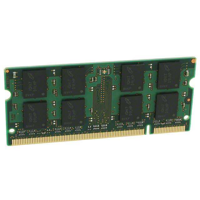
| 描述 | MODULE DDR2 SDRAM 2GB 200SODIMM |
| 产品分类 | |
| 品牌 | Micron Technology Inc |
| 数据手册 | |
| 产品图片 |
|
| 产品型号 | MT16HTF25664HZ-800H1 |
| PCN过时产品 | |
| rohs | 无铅 / 符合限制有害物质指令(RoHS)规范要求 |
| 产品系列 | - |
| 其它名称 | 557-1477 |
| 存储器类型 | DDR2 SDRAM |
| 存储容量 | 2GB |
| 封装/外壳 | 200-SODIMM |
| 标准包装 | 100 |
| 速度 | 800MT/s |


- 商务部:美国ITC正式对集成电路等产品启动337调查
- 曝三星4nm工艺存在良率问题 高通将骁龙8 Gen1或转产台积电
- 太阳诱电将投资9.5亿元在常州建新厂生产MLCC 预计2023年完工
- 英特尔发布欧洲新工厂建设计划 深化IDM 2.0 战略
- 台积电先进制程称霸业界 有大客户加持明年业绩稳了
- 达到5530亿美元!SIA预计今年全球半导体销售额将创下新高
- 英特尔拟将自动驾驶子公司Mobileye上市 估值或超500亿美元
- 三星加码芯片和SET,合并消费电子和移动部门,撤换高东真等 CEO
- 三星电子宣布重大人事变动 还合并消费电子和移动部门
- 海关总署:前11个月进口集成电路产品价值2.52万亿元 增长14.8%


PDF Datasheet 数据手册内容提取
1GB, 2GB, 4GB (x64, DR) 200-Pin DDR2 SDRAM SODIMM Features DDR2 SDRAM SODIMM MT16HTF12864HZ – 1GB MT16HTF25664HZ – 2GB MT16HTF51264HZ – 4GB Features Figure 1: 200-Pin SODIMM (MO-224 R/C E) • 200-pin, small-outline dual in-line memory module Module Height: 30mm (1.181 in.) (SODIMM) • Fast data transfer rates: PC2-3200, PC2-4200, PC2-5300, or PC2-6400 • 1GB (128 Meg x 64), 2GB (256 Meg x 64) or 4GB (512 Meg x 64) • V = V = 1.8V DD DDQ • V = 1.7–3.6V DDSPD • JEDEC-standard 1.8V I/O (SSTL_18-compatible) • Differential data strobe (DQS, DQS#) option Options Marking • 4n-bit prefetch architecture • Operating temperature • Multiple internal device banks for concurrent – Commercial (0°C ≤ T ≤ +70°C) None operation A – Industrial (–40°C ≤ T ≤ +85°C)1 I • Programmable CAS latency (CL) A • Package • Posted CAS additive latency (AL) – 200-pin DIMM (halogen-free) Z • WRITE latency = READ latency - 1 tCK • Frequency/CL2 • Programmable burst lengths (BL): 4 or 8 – 1.87ns @ CL = 7 (DDR2-1066) -1GA • Adjustable data-output drive strength – 2.5ns @ CL = 5 (DDR2-800) -80E – 2.5ns @ CL = 6 (DDR2-800) -800 • 64ms, 8192-cycle refresh – 3ns @ CL = 5 (DDR2-667) -667 • On-die termination (ODT) • Halogen-free Notes: 1. Contact Micron for industrial temperature module offerings. • Serial presence detect (SPD) with EEPROM 2. CL = CAS (READ) latency. • Gold edge contacts 3. Not recommended for new designs. • Dual rank Table 1: Key Timing Parameters Speed Industry Data Rate (MT/s) tRCD tRP tRC Grade Nomenclature CL = 7 CL = 6 CL = 5 CL = 4 CL = 3 (ns) (ns) (ns) -1GA PC2-8500 1066 800 667 533 400 13.125 13.125 58.125 -80E PC2-6400 800 800 533 400 12.5 12.5 57.5 -800 PC2-6400 800 667 533 400 15 15 60 -667 PC2-5300 – 667 553 400 15 15 60 -53E PC2-4200 – – 553 400 15 15 55 -40E PC2-3200 – – 400 400 15 15 55 PDF: 09005aef8339ef97 1 Micron Technology, Inc. reserves the right to change products or specifications without notice. htf16c128_256_512x64hz.pdf - Rev. D 4/14 EN © 2008 Micron Technology, Inc. All rights reserved. Products and specifications discussed herein are subject to change by Micron without notice.
1GB, 2GB, 4GB (x64, DR) 200-Pin DDR2 SDRAM SODIMM Features Table 2: Addressing Parameter 1GB 2GB 4GB Refresh count 8K 8K 8K Row address 16K A[13:0] 16K A[13:0] 32K A[14:0] Device bank address 4 BA[1:0] 8 BA[2:0] 8 BA[2:0] Device configuration 512Mb (64 Meg x 8) 1Gb (128 Meg x 8) 2Gb (256 Meg x 8) Column address 1K A[9:0] 1K A[9:0] 1K A[9:0] Module rank address 2 S#[1:0] 2 S#[1:0] 2 S#[1:0] Table 3: Part Numbers and Timing Parameters – 1GB Modules Base device: MT47H64M8,1 512Mb DDR2 SDRAM Module Module Memory Clock/ Clock Cycles Part Number2 Density Configuration Bandwidth Data Rate (CL-tRCD-tRP) MT16HTF12864H(I)Z-80E__ 1GB 128 Meg x 64 6.4 GB/s 2.5ns/800 MT/s 5-5-5 MT16HTF12864H(I)Z-800__ 1GB 128 Meg x 64 6.4 GB/s 2.5ns/800 MT/s 6-6-6 MT16HTF12864H(I)Z-667__ 1GB 128 Meg x 64 5.3 GB/s 3.0ns/667 MT/s 5-5-5 Table 4: Part Numbers and Timing Parameters – 2GB Modules Base device: MT47H128M8,1 1Gb DDR2 SDRAM Module Module Memory Clock/ Clock Cycles Part Number2 Density Configuration Bandwidth Data Rate (CL-tRCD-tRP) MT16HTF25664H(I)Z-1GA__ 2GB 256 Meg x 64 8.5 GB/s 1.87ns/1066 MT/s 7-7-7 MT16HTF25664H(I)Z-80E__ 2GB 256 Meg x 64 6.4 GB/s 2.5ns/800 MT/s 5-5-5 MT16HTF25664H(I)Z-800__ 2GB 256 Meg x 64 6.4 GB/s 2.5ns/800 MT/s 6-6-6 MT16HTF25664H(I)Z-667__ 2GB 256 Meg x 64 5.3 GB/s 3.0ns/667 MT/s 5-5-5 Table 5: Part Numbers and Timing Parameters – 2GB Modules Base device: MT47H256M8,1 2Gb DDR2 SDRAM Module Module Memory Clock/ Clock Cycles Part Number2 Density Configuration Bandwidth Data Rate (CL-tRCD-tRP) MT16HTF51264H(I)Z-1GA__ 4GB 512 Meg x 64 8.5 GB/s 1.87ns/1066 MT/s 7-7-7 MT16HTF51264H(I)Z-80E__ 4GB 512 Meg x 64 6.4 GB/s 2.5ns/800 MT/s 5-5-5 MT16HTF51264H(I)Z-800__ 4GB 512Meg x 64 6.4 GB/s 2.5ns/800 MT/s 6-6-6 MT16HTF51264H(I)Z-667__ 4GB 512 Meg x 64 5.3 GB/s 3.0ns/667 MT/s 5-5-5 Notes: 1. The data sheet for the base device can be found on Micron’s Web site. 2. All part numbers end with a two-place code (not shown) that designates component and PCB revisions. Consult factory for current revision codes. Example: MT16HTF25664HZ-80EM1. PDF: 09005aef8339ef97 2 Micron Technology, Inc. reserves the right to change products or specifications without notice. htf16c128_256_512x64hz.pdf - Rev. D 4/14 EN © 2008 Micron Technology, Inc. All rights reserved.
1GB, 2GB, 4GB (x64, DR) 200-Pin DDR2 SDRAM SODIMM Pin Assignments Pin Assignments Table 6: Pin Assignments 200-Pin DDR2 SODIMM Front 200-Pin DDR2 SODIMM Back Pin Symbol Pin Symbol Pin Symbol Pin Symbol Pin Symbol Pin Symbol Pin Symbol Pin Symbol 1 V 51 DQS2 101 A1 151 DQ42 2 V 52 DM2 102 A0 152 DQ46 REF SS 3 V 53 V 103 V 153 DQ43 4 DQ4 54 V 104 V 154 DQ47 SS SS DD SS DD 5 DQ0 55 DQ18 105 A10 155 V 6 DQ5 56 DQ22 106 BA1 156 V SS SS 7 DQ1 57 DQ19 107 BA0 157 DQ48 8 V 58 DQ23 108 RAS# 158 DQ52 SS 9 V 59 V 109 WE# 159 DQ49 10 DM0 60 V 110 S0# 160 DQ53 SS SS SS 11 DQS0# 61 DQ24 111 V 161 V 12 V 62 DQ28 112 V 162 V DD SS SS DD SS 13 DQS0 63 DQ25 113 CAS# 163 NC 14 DQ6 64 DQ29 114 ODT0 164 CK1 15 V 65 V 115 S1# 165 V 16 DQ7 66 V 116 A13 166 CK1# SS SS SS SS 17 DQ2 67 DM3 117 V 167 DQS6# 18 V 68 DQS3# 118 V 168 V DD SS DD SS 19 DQ3 69 NC 119 ODT1 169 DQS6 20 DQ12 70 DQS3 120 NC 170 DM6 21 V 71 V 121 V 171 V 22 DQ13 72 V 122 V 172 V SS SS SS SS SS SS SS 23 DQ8 73 DQ26 123 DQ32 173 DQ50 24 V 74 DQ30 124 DQ36 174 DQ54 SS 25 DQ9 75 DQ27 125 DQ33 175 DQ51 26 DM1 76 DQ31 126 DQ37 176 DQ55 27 V 77 V 127 V 177 V 28 V 78 V 128 V 178 V SS SS SS SS SS SS SS SS 29 DQS1# 79 CKE0 129 DQS4# 179 DQ56 30 CK0 80 CKE1 130 DM4 180 DQ60 31 DQS1 81 V 131 DQS4 181 DQ57 32 CK0# 82 V 132 V 182 DQ61 DD DD SS 33 V 83 NC 133 V 183 V 34 V 84 NC 134 DQ38 184 V SS SS SS SS SS 35 DQ10 85 NC/BA21 135 DQ34 185 DM7 36 DQ14 86 NC/A142 136 DQ39 186 DQS7# 37 DQ11 V V 137 DQ35 187 V 38 DQ15 88 V 138 V 188 DQS7 DD DD SS DD SS 39 V 89 A12 139 V 189 DQ58 40 V 90 A11 140 DQ44 190 V SS SS SS SS 41 V 91 A9 141 DQ40 191 DQ59 42 V 92 A7 142 DQ45 192 DQ62 SS SS 43 DQ16 93 A8 143 DQ41 193 V 44 DQ20 94 A6 144 V 194 DQ63 SS SS 45 DQ17 95 V 145 V 195 SDA 46 DQ21 96 V 146 DQS5# 196 V DD SS DD SS 47 V 97 A5 147 DM5 197 SCL 48 V 98 A4 148 DQS5 198 SA0 SS SS 49 DQS2# 99 A3 149 V 199 V 50 NC 100 A2 150 V 200 SA1 SS DDSPD SS Notes: 1. Pin 85 is NC for 1GB and BA2 for 2GB, 4GB. 2. Pin 86 is NC for 1GB, 2GB and A14 for 4GB. PDF: 09005aef8339ef97 3 Micron Technology, Inc. reserves the right to change products or specifications without notice. htf16c128_256_512x64hz.pdf - Rev. D 4/14 EN © 2008 Micron Technology, Inc. All rights reserved.
1GB, 2GB, 4GB (x64, DR) 200-Pin DDR2 SDRAM SODIMM Pin Descriptions Pin Descriptions The pin description table below is a comprehensive list of all possible pins for all DDR2 modules. All pins listed may not be supported on this module. See Pin Assignments for information specific to this module. Table 7: Pin Descriptions Symbol Type Description Ax Input Address inputs: Provide the row address for ACTIVE commands, and the column ad- dress and auto precharge bit (A10) for READ/WRITE commands, to select one location out of the memory array in the respective bank. A10 sampled during a PRECHARGE command determines whether the PRECHARGE applies to one bank (A10 LOW, bank selected by BAx) or all banks (A10 HIGH). The address inputs also provide the op-code during a LOAD MODE command. See the Pin Assignments Table for density-specific addressing information. BAx Input Bank address inputs: Define the device bank to which an ACTIVE, READ, WRITE, or PRECHARGE command is being applied. BA define which mode register (MR0, MR1, MR2, and MR3) is loaded during the LOAD MODE command. CKx, Input Clock: Differential clock inputs. All control, command, and address input signals are CK#x sampled on the crossing of the positive edge of CK and the negative edge of CK#. CKEx Input Clock enable: Enables (registered HIGH) and disables (registered LOW) internal circui- try and clocks on the DDR2 SDRAM. DMx Input Data mask (x8 devices only): DM is an input mask signal for write data. Input data is masked when DM is sampled HIGH, along with that input data, during a write ac- cess. Although DM pins are input-only, DM loading is designed to match that of the DQ and DQS pins. ODTx Input On-die termination: Enables (registered HIGH) and disables (registered LOW) termi- nation resistance internal to the DDR2 SDRAM. When enabled in normal operation, ODT is only applied to the following pins: DQ, DQS, DQS#, DM, and CB. The ODT input will be ignored if disabled via the LOAD MODE command. Par_In Input Parity input: Parity bit for Ax, RAS#, CAS#, and WE#. RAS#, CAS#, WE# Input Command inputs: RAS#, CAS#, and WE# (along with S#) define the command being entered. RESET# Input Reset: Asynchronously forces all registered outputs LOW when RESET# is LOW. This signal can be used during power-up to ensure that CKE is LOW and DQ are High-Z. S#x Input Chip select: Enables (registered LOW) and disables (registered HIGH) the command decoder. SAx Input Serial address inputs: Used to configure the SPD EEPROM address range on the I2C bus. SCL Input Serial clock for SPD EEPROM: Used to synchronize communication to and from the SPD EEPROM on the I2C bus. CBx I/O Check bits. Used for system error detection and correction. DQx I/O Data input/output: Bidirectional data bus. DQSx, I/O Data strobe: Travels with the DQ and is used to capture DQ at the DRAM or the con- DQS#x troller. Output with read data; input with write data for source synchronous opera- tion. DQS# is only used when differential data strobe mode is enabled via the LOAD MODE command. PDF: 09005aef8339ef97 4 Micron Technology, Inc. reserves the right to change products or specifications without notice. htf16c128_256_512x64hz.pdf - Rev. D 4/14 EN © 2008 Micron Technology, Inc. All rights reserved.
1GB, 2GB, 4GB (x64, DR) 200-Pin DDR2 SDRAM SODIMM Pin Descriptions Table 7: Pin Descriptions (Continued) Symbol Type Description SDA I/O Serial data: Used to transfer addresses and data into and out of the SPD EEPROM on the I2C bus. RDQSx, Output Redundant data strobe (x8 devices only): RDQS is enabled/disabled via the LOAD RDQS#x MODE command to the extended mode register (EMR). When RDQS is enabled, RDQS is output with read data only and is ignored during write data. When RDQS is disa- bled, RDQS becomes data mask (see DMx). RDQS# is only used when RDQS is enabled and differential data strobe mode is enabled. Err_Out# Output Parity error output: Parity error found on the command and address bus. (open drain) V /V Supply Power supply: 1.8V ±0.1V. The component V and V are connected to the mod- DD DDQ DD DDQ ule V . DD V Supply SPD EEPROM power supply: 1.7–3.6V. DDSPD V Supply Reference voltage: V /2. REF DD V Supply Ground. SS NC – No connect: These pins are not connected on the module. NF – No function: These pins are connected within the module, but provide no functional- ity. NU – Not used: These pins are not used in specific module configurations/operations. RFU – Reserved for future use. PDF: 09005aef8339ef97 5 Micron Technology, Inc. reserves the right to change products or specifications without notice. htf16c128_256_512x64hz.pdf - Rev. D 4/14 EN © 2008 Micron Technology, Inc. All rights reserved.
1GB, 2GB, 4GB (x64, DR) 200-Pin DDR2 SDRAM SODIMM Functional Block Diagram – 1GB, 2GB Functional Block Diagram – 1GB, 2GB Figure 2: Functional Block Diagram – 1GB, 2GB S1# S0# DQS0# DQS4# DQS0 DQS4 DM0 DM4 DM CS# DQ DQS# DM CS# DQ DQS# DM CS# DQ DQS# DM CS# DQ DQS# DQ0 DQ DQ DQ32 DQ DQ DQ1 DQ DQ DQ33 DQ DQ DQ2 DQ U1 DQ U14 DQ34 DQ U4 DQ U11 DQ3 DQ DQ DQ35 DQ DQ DQ4 DQ DQ DQ36 DQ DQ DQ5 DQ DQ DQ37 DQ DQ DQ6 DQ DQ DQ38 DQ DQ DQ7 DQ DQ DQ39 DQ DQ DQS1# DQS5# DQS1 DQS5 DM1 DM5 DM CS# DQ DQS# DM CS# DQ DQS# DM CS# DQ DQS# DM CS# DQ DQS# DQ8 DQ DQ DQ40 DQ DQ DQ9 DQ DQ DQ41 DQ DQ DDQQ1101 DDQQ U6 DDQQ U18 DDQQ4423 DDQQ U8 DDQQ U16 DQ12 DQ DQ DQ44 DQ DQ DQ13 DQ DQ DQ45 DQ DQ DQ14 DQ DQ DQ46 DQ DQ DQ15 DQ DQ DQ47 DQ DQ DQS2# DQS6# DQS2 DQS6 DM2 DM6 DM CS# DQ DQS# DM CS# DQ DQS# DM CS# DQ DQS# DM CS# DQ DQS# DQ16 DQ DQ DQ48 DQ DQ DQ17 DQ DQ DQ49 DQ DQ DQ18 DQ U2 DQ U13 DQ50 DQ U5 DQ U10 DQ19 DQ DQ DQ51 DQ DQ DQ20 DQ DQ DQ52 DQ DQ DQ21 DQ DQ DQ53 DQ DQ DQ22 DQ DQ DQ54 DQ DQ DQ23 DQ DQ DQ55 DQ DQ DQS3# DQS7# DQS3 DQS7 DM3 DM7 DM CS# DQ DQS# DM CS# DQ DQS# DM CS# DQ DQS# DM CS# DQ DQS# DQ24 DQ DQ DQ56 DQ DQ DQ25 DQ DQ DQ57 DQ DQ DQ26 DQ U7 DQ U17 DQ58 DQ U9 DQ U15 DQ27 DQ DQ DQ59 DQ DQ DQ28 DQ DQ DQ60 DQ DQ DQ29 DQ DQ DQ61 DQ DQ DQ30 DQ DQ DQ62 DQ DQ DQ31 DQ DQ DQ63 DQ DQ U3 Rank 0 = U1, U2, U4–U9 BA[2/1:0] BA[2/1:0]: DDR2 SDRAM SPD/EEPROM Rank 1 = U10, U11, U13–U18 A[13:0] A[13:0]: DDR2 SDRAM SCL SDA RAS# RAS#: DDR2 SDRAM WPA0 A1 A2 CWAES## CWAES##:: DDDDRR22 SSDDRRAAMM VSSSA0 SA1VSS CCKK00# UU11,3 U, U2,1 U4,6 U, U177, U18 CKE0 CKE0: Rank 0 VDDSPD SPD/EEPROM CKE1 CKE1: Rank 1 VDD DDR2 SDRAM OODDTT01 OODDTT01:: RRaannkk 01 VREF DDR2 SDRAM CCKK11# UU41,0 U, U5,1 U1,8 U, U159, U16 VSS DDR2 SDRAM, EEPROM PDF: 09005aef8339ef97 6 Micron Technology, Inc. reserves the right to change products or specifications without notice. htf16c128_256_512x64hz.pdf - Rev. D 4/14 EN © 2008 Micron Technology, Inc. All rights reserved.
1GB, 2GB, 4GB (x64, DR) 200-Pin DDR2 SDRAM SODIMM Functional Block Diagram – 4GB Functional Block Diagram – 4GB Figure 3: Functional Block Diagram – 4GB S1# S0# DQS0# DQS4# DQS0 DQS4 DM0 DM4 DM CS# DQ DQS# DM CS# DQ DQS# DM CS# DQ DQS# DM CS# DQ DQS# DQ0 DQ DQ DQ32 DQ DQ DQ1 DQ DQ DQ33 DQ DQ DQ2 DQ U1 DQ U14 DQ34 DQ U5 DQ U12 DQ3 DQ DQ DQ35 DQ DQ DQ4 DQ DQ DQ36 DQ DQ DQ5 DQ DQ DQ37 DQ DQ DQ6 DQ DQ DQ38 DQ DQ DQ7 DQ DQ DQ39 DQ DQ DQS1# DQS5# DQS1 DQS5 DM1 DM5 DM CS# DQ DQS# DM CS# DQ DQS# DM CS# DQ DQS# DM CS# DQ DQS# DQ8 DQ DQ DQ40 DQ DQ DQ9 DQ DQ DQ41 DQ DQ DDQQ1101 DDQQ U7 DDQQ U18 DDQQ4423 DDQQ U9 DDQQ U16 DQ12 DQ DQ DQ44 DQ DQ DQ13 DQ DQ DQ45 DQ DQ DQ14 DQ DQ DQ46 DQ DQ DQ15 DQ DQ DQ47 DQ DQ DQS2# DQS6# DQS2 DQS6 DM2 DM6 DM CS# DQ DQS# DM CS# DQ DQS# DM CS# DQ DQS# DM CS# DQ DQS# DQ16 DQ DQ DQ48 DQ DQ DQ17 DQ DQ DQ49 DQ DQ DQ18 DQ U2 DQ U13 DQ50 DQ U6 DQ U11 DQ19 DQ DQ DQ51 DQ DQ DQ20 DQ DQ DQ52 DQ DQ DQ21 DQ DQ DQ53 DQ DQ DQ22 DQ DQ DQ54 DQ DQ DQ23 DQ DQ DQ55 DQ DQ DQS3# DQS7# DQS3 DQS7 DM3 DM7 DM CS# DQ DQS# DM CS# DQ DQS# DM CS# DQ DQS# DM CS# DQ DQS# DQ24 DQ DQ DQ56 DQ DQ DQ25 DQ DQ DQ57 DQ DQ DQ26 DQ U8 DQ U17 DQ58 DQ U10 DQ U15 DQ27 DQ DQ DQ59 DQ DQ DQ28 DQ DQ DQ60 DQ DQ DQ29 DQ DQ DQ61 DQ DQ DQ30 DQ DQ DQ62 DQ DQ DQ31 DQ DQ DQ63 DQ DQ U4 Rank 0 = U1, U2, U5–U10 BA[2:0] BA[2:0]: DDR2 SDRAM SPD/EEPROM Rank 1 = U11–U18 A[14:0] A[14:0]: DDR2 SDRAM SCL SDA RAS# RAS#: DDR2 SDRAM WPA0 A1 A2 CWAES## CWAES##:: DDDDRR22 SSDDRRAAMM VSSSA0 SA1 VSS CCKK00# UU11,3 U, U2,1 U4,7 U, U178, U18 CKE0 CKE0: Rank 0 VDDSPD SPD/EEPROM CKE1 CKE1: Rank 1 VDD DDR2 SDRAM OODDTT01 OODDTT01:: RRaannkk 01 VREF DDR2 SDRAM CCKK11# UU51,1 U, U6,1 U2,9 U, U151,0 U 16 VSS DDR2 SDRAM, EEPROM PDF: 09005aef8339ef97 7 Micron Technology, Inc. reserves the right to change products or specifications without notice. htf16c128_256_512x64hz.pdf - Rev. D 4/14 EN © 2008 Micron Technology, Inc. All rights reserved.
1GB, 2GB, 4GB (x64, DR) 200-Pin DDR2 SDRAM SODIMM General Description General Description DDR2 SDRAM modules are high-speed, CMOS dynamic random access memory mod- ules that use internally configured 4 or 8-bank DDR2 SDRAM devices. DDR2 SDRAM modules use DDR architecture to achieve high-speed operation. DDR2 architecture is essentially a 4n-prefetch architecture with an interface designed to transfer two data words per clock cycle at the I/O pins. A single read or write access for the DDR2 SDRAM module effectively consists of a single 4n-bit-wide, one-clock-cycle data transfer at the internal DRAM core and eight corresponding n-bit-wide, one-half-clock-cycle data transfers at the I/O pins. DDR2 modules use two sets of differential signals: DQS, DQS# to capture data and CK and CK# to capture commands, addresses, and control signals. Differential clocks and data strobes ensure exceptional noise immunity for these signals and provide precise crossing points to capture input signals. A bidirectional data strobe (DQS, DQS#) is transmitted externally, along with data, for use in data capture at the receiver. DQS is a strobe transmitted by the DDR2 SDRAM device during READs and by the memory con- troller during WRITEs. DQS is edge-aligned with data for READs and center-aligned with data for WRITEs. DDR2 SDRAM modules operate from a differential clock (CK and CK#); the crossing of CK going HIGH and CK# going LOW will be referred to as the positive edge of CK. Com- mands (address and control signals) are registered at every positive edge of CK. Input data is registered on both edges of DQS, and output data is referenced to both edges of DQS, as well as to both edges of CK. Serial Presence-Detect EEPROM Operation DDR2 SDRAM modules incorporate serial presence-detect. The SPD data is stored in a 256-byte EEPROM. The first 128 bytes are programmed by Micron to identify the mod- ule type and various SDRAM organizations and timing parameters. The remaining 128 bytes of storage are available for use by the customer. System READ/WRITE operations between the master (system logic) and the slave EEPROM device occur via a standard I2C bus using the DIMM’s SCL (clock) SDA (data), and SA (address) pins. Write protect (WP) is connected to V , permanently disabling hardware write protection. SS PDF: 09005aef8339ef97 8 Micron Technology, Inc. reserves the right to change products or specifications without notice. htf16c128_256_512x64hz.pdf - Rev. D 4/14 EN © 2008 Micron Technology, Inc. All rights reserved.
1GB, 2GB, 4GB (x64, DR) 200-Pin DDR2 SDRAM SODIMM Electrical Specifications Electrical Specifications Stresses greater than those listed may cause permanent damage to the module. This is a stress rating only, and functional operation of the module at these or any other condi- tions outside those indicated in the device data sheet are not implied. Exposure to abso- lute maximum rating conditions for extended periods may adversely affect reliability. Table 8: Absolute Maximum Ratings Symbol Parameter Min Max Units V V supply voltage relative to V –1.0 2.3 V DD DD SS V , V Voltage on any pin relative to V –0.5 2.3 V IN OUT SS I Input leakage current; Any input 0V ≤ V ≤ Address inputs, RAS#, CAS#, –80 80 µA I IN V ; V input 0V ≤ V ≤ 0.95V; (All other WE#, BA DD REF IN pins not under test = 0V) S#, CKE, ODT, CK, CK# –40 40 DM –10 10 I Output leakage current; 0V ≤ V ; DQ and DQ, DQS, DQS# –10 10 µA OZ OUT ODT are disabled I V leakage current; V = valid V level –32 32 µA VREF REF REF REF T Module ambient operating temperature Commercial 0 70 °C A Industrial –40 85 °C T 1 DDR2 SDRAM component operating tem- Commercial 0 85 °C C perature2 Industrial –40 95 °C Notes: 1. The refresh rate is required to double when TC exceeds 85°C. 2. For further information, refer to technical note TN-00-08: "Thermal Applications," avail- able on Micron’s Web site. PDF: 09005aef8339ef97 9 Micron Technology, Inc. reserves the right to change products or specifications without notice. htf16c128_256_512x64hz.pdf - Rev. D 4/14 EN © 2008 Micron Technology, Inc. All rights reserved.
1GB, 2GB, 4GB (x64, DR) 200-Pin DDR2 SDRAM SODIMM DRAM Operating Conditions DRAM Operating Conditions Recommended AC operating conditions are given in the DDR2 component data sheets. Component specifications are available on Micron's Web site. Module speed grades cor- relate with component speed grades. Table 9: Module and Component Speed Grades DDR2 components may exceed the listed module speed grades; module may not be available in all listed speed grades Module Speed Grade Component Speed Grade -1GA -187E -80E -25E -800 -25 -667 -3 -53E -37E -40E -5E Design Considerations Simulations Micron memory modules are designed to optimize signal integrity through carefully de- signed terminations, controlled board impedances, routing topologies, trace length matching, and decoupling. However, good signal integrity starts at the system level. Mi- cron encourages designers to simulate the signal characteristics of the system's memo- ry bus to ensure adequate signal integrity of the entire memory system. Power Operating voltages are specified at the DRAM, not at the edge connector of the module. Designers must account for any system voltage drops at anticipated power levels to en- sure the required supply voltage is maintained. PDF: 09005aef8339ef97 10 Micron Technology, Inc. reserves the right to change products or specifications without notice. htf16c128_256_512x64hz.pdf - Rev. D 4/14 EN © 2008 Micron Technology, Inc. All rights reserved.
1GB, 2GB, 4GB (x64, DR) 200-Pin DDR2 SDRAM SODIMM IDD Specifications IDD Specifications Table 10: DDR2 I Specifications and Conditions – 1GB (Die Revision G) DD Values shown for MT47H64M8 DDR2 SDRAM only and are computed from values specified in the 512Mb (64 Meg x 8) com- ponent data sheet -80E/ Parameter Symbol -800 -667 Units Operating one bank active-precharge current:tCK = tCK (I ), tRC = tRC (I ), tRAS = I 1 576 536 mA DD DD DD0 tRAS MIN (I ); CKE is HIGH, S# is HIGH between valid commands; Address bus inputs are DD switching; Data bus inputs are switching Operating one bank active-read-precharge current: I = 0mA; BL = 4, CL = CL I 1 656 616 mA OUT DD1 (I ), AL = 0; tCK = tCK (I ), tRC = tRC (I ), tRAS = tRAS MIN (I ), tRCD = tRCD (I ); CKE DD DD DD DD DD is HIGH, S# is HIGH between valid commands; Address bus inputs are switching; Data pattern is same as I DD4W Precharge power-down current: All device banks idle; tCK = tCK (I ); CKE is LOW; I 2 112 112 mA DD DD2P Other control and address bus inputs are stable; Data bus inputs are floating Precharge quiet standby current: All device banks idle; tCK = tCK (I ); CKE is HIGH, I 2 384 352 mA DD DD2Q S# is HIGH; Other control and address bus inputs are stable; Data bus inputs are floating Precharge standby current: All device banks idle; tCK = tCK (I ); CKE is HIGH, S# is I 2 448 400 mA DD DD2N HIGH; Other control and address bus inputs are switching; Data bus inputs are switching Active power-down current: All device banks open; tCK Fast PDN exit MR[12] = 0 I 2 288 240 mA DD3P = tCK (IDD); CKE is LOW; Other control and address bus in- Slow PDN exit MR[12] = 1 144 144 puts are stable; Data bus inputs are floating Active standby current: All device banks open; tCK = tCK (I ), tRAS = tRAS MAX (I ), I 2 528 480 mA DD DD DD3N tRP = tRP (I ); CKE is HIGH, S# is HIGH between valid commands; Other control and ad- DD dress bus inputs are switching; Data bus inputs are switching Operating burst write current: All device banks open; Continuous burst writes; BL = I 1 1056 976 mA DD4W 4, CL = CL (I ), AL = 0; tCK = tCK (I ), tRAS = tRAS MAX (I ), tRP = tRP (I ); CKE is DD DD DD DD HIGH, S# is HIGH between valid commands; Address bus inputs are switching; Data bus inputs are switching Operating burst read current: All device banks open; Continuous burst read, I = I 1 1016 936 mA OUT DD4R 0mA; BL = 4, CL = CL (I ), AL = 0; tCK = tCK (I ), tRAS = tRAS MAX (I ), tRP = tRP (I ); DD DD DD DD CKE is HIGH, S# is HIGH between valid commands; Address bus inputs are switching; Da- ta bus inputs are switching Burst refresh current:tCK = tCK (I ); REFRESH command at every tRFC (I ) interval; I 2 816 776 mA DD DD DD5 CKE is HIGH, S# is HIGH between valid commands; Other control and address bus inputs are switching; Data bus inputs are switching Self refresh current: CK and CK# at 0V; CKE ≤ 0.2V; Other control and address bus in- I 2 112 112 mA DD6 puts are floating; Data bus inputs are floating Operating bank interleave read current: All device banks interleaving reads; I = I 1 1256 1176 mA OUT DD7 0mA; BL = 4, CL = CL (I ), AL = tRCD (I ) - 1 × tCK (I ); tCK = tCK (I ), tRC = tRC (I ), DD DD DD DD DD tRRD = tRRD (I ), tRCD = tRCD (I ); CKE is HIGH, S# is HIGH between valid commands; DD DD Address bus inputs are stable during deselects; Data bus inputs are switching Notes: 1. Value calculated as one module rank in this operating condition; all other module ranks in I (CKE LOW) mode. DD2P 2. Value calculated reflects all module ranks in this operating condition. PDF: 09005aef8339ef97 11 Micron Technology, Inc. reserves the right to change products or specifications without notice. htf16c128_256_512x64hz.pdf - Rev. D 4/14 EN © 2008 Micron Technology, Inc. All rights reserved.
1GB, 2GB, 4GB (x64, DR) 200-Pin DDR2 SDRAM SODIMM IDD Specifications Table 11: DDR2 I Specifications and Conditions – 2GB (Die Revision H) DD Values shown for MT47H128M8 DDR2 SDRAM only and are computed from values specified in the 1Gb (128 Meg x 8) com- ponent data sheet -80E/ Parameter Symbol -1GA -800 -667 Units Operating one bank active-precharge current:tCK = tCK (I ), tRC = tRC (I ), I 1 656 576 536 mA DD DD DD0 tRAS = tRAS MIN (I ); CKE is HIGH, S# is HIGH between valid commands; Address DD bus inputs are switching; Data bus inputs are switching Operating one bank active-read-precharge current: I = 0mA; BL = 4, CL = I 1 736 656 616 mA OUT DD1 CL (I ), AL = 0; tCK = tCK (I ), tRC = tRC (I ), tRAS = tRAS MIN (I ), tRCD = tRCD DD DD DD DD (I ); CKE is HIGH, S# is HIGH between valid commands; Address bus inputs are DD switching; Data pattern is same as I DD4W Precharge power-down current: All device banks idle; tCK = tCK (I ); CKE is I 2 112 112 112 mA DD DD2P LOW; Other control and address bus inputs are stable; Data bus inputs are float- ing Precharge quiet standby current: All device banks idle; tCK = tCK (I ); CKE is I 2 448 384 384 mA DD DD2Q HIGH, S# is HIGH; Other control and address bus inputs are stable; Data bus inputs are floating Precharge standby current: All device banks idle; tCK = tCK (I ); CKE is HIGH, I 2 544 448 384 mA DD DD2N S# is HIGH; Other control and address bus inputs are switching; Data bus inputs are switching Active power-down current: All device banks open; Fast PDN exit MR[12] = 0 I 2 368 320 240 mA DD3P tCK = tCK (IDD); CKE is LOW; Other control and address Slow PDN exit MR[12] = 1 160 160 160 bus inputs are stable; Data bus inputs are floating Active standby current: All device banks open; tCK = tCK (I ), tRAS = tRAS I 2 640 528 480 mA DD DD3N MAX (I ), tRP = tRP (I ); CKE is HIGH, S# is HIGH between valid commands; Oth- DD DD er control and address bus inputs are switching; Data bus inputs are switching Operating burst write current: All device banks open; Continuous burst writes; I 1 1216 1056 976 mA DD4W BL = 4, CL = CL (I ), AL = 0; tCK = tCK (I ), tRAS = tRAS MAX (I ), tRP = tRP (I ); DD DD DD DD CKE is HIGH, S# is HIGH between valid commands; Address bus inputs are switch- ing; Data bus inputs are switching Operating burst read current: All device banks open; Continuous burst read, I 1 1176 1016 936 mA DD4R I = 0mA; BL = 4, CL = CL (I ), AL = 0; tCK = tCK (I ), tRAS = tRAS MAX (I ), OUT DD DD DD tRP = tRP (I ); CKE is HIGH, S# is HIGH between valid commands; Address bus in- DD puts are switching; Data bus inputs are switching Burst refresh current:tCK = tCK (I ); REFRESH command at every tRFC (I ) in- I 2 1296 1216 1176 mA DD DD DD5 terval; CKE is HIGH, S# is HIGH between valid commands; Other control and ad- dress bus inputs are switching; Data bus inputs are switching Self refresh current: CK and CK# at 0V; CKE ≤ 0.2V; Other control and address I 2 112 112 112 mA DD6 bus inputs are floating; Data bus inputs are floating Operating bank interleave read current: All device banks interleaving reads; I 1 1816 1736 1536 mA DD7 I = 0mA; BL = 4, CL = CL (I ), AL = tRCD (I ) - 1 × tCK (I ); tCK = tCK (I ), tRC OUT DD DD DD DD = tRC (I ), tRRD = tRRD (I ), tRCD = tRCD (I ); CKE is HIGH, S# is HIGH between DD DD DD valid commands; Address bus inputs are stable during deselects; Data bus inputs are switching Notes: 1. Value calculated as one module rank in this operating condition; all other module ranks in I (CKE LOW) mode. DD2P PDF: 09005aef8339ef97 12 Micron Technology, Inc. reserves the right to change products or specifications without notice. htf16c128_256_512x64hz.pdf - Rev. D 4/14 EN © 2008 Micron Technology, Inc. All rights reserved.
1GB, 2GB, 4GB (x64, DR) 200-Pin DDR2 SDRAM SODIMM IDD Specifications 2. Value calculated reflects all module ranks in this operating condition. Table 12: DDR2 I Specifications and Conditions – 2GB (Die Revision M) DD Values shown for MT47H128M8 DDR2 SDRAM only and are computed from values specified in the 1Gb (128 Meg x 8) com- ponent data sheet -80E/ Parameter Symbol -1GA -800 -667 Units Operating one bank active-precharge current:tCK = tCK (I ), tRC = tRC (I ), I 1 680 600 560 mA DD DD DD0 tRAS = tRAS MIN (I ); CKE is HIGH, S# is HIGH between valid commands; Address DD bus inputs are switching; Data bus inputs are switching Operating one bank active-read-precharge current: I = 0mA; BL = 4, CL = I 1 760 680 640 mA OUT DD1 CL (I ), AL = 0; tCK = tCK (I ), tRC = tRC (I ), tRAS = tRAS MIN (I ), tRCD = tRCD DD DD DD DD (I ); CKE is HIGH, S# is HIGH between valid commands; Address bus inputs are DD switching; Data pattern is same as I DD4W Precharge power-down current: All device banks idle; tCK = tCK (I ); CKE is I 2 160 160 160 mA DD DD2P LOW; Other control and address bus inputs are stable; Data bus inputs are float- ing Precharge quiet standby current: All device banks idle; tCK = tCK (I ); CKE is I 2 448 384 384 mA DD DD2Q HIGH, S# is HIGH; Other control and address bus inputs are stable; Data bus in- puts are floating Precharge standby current: All device banks idle; tCK = tCK (I ); CKE is HIGH, I 2 544 448 384 mA DD DD2N S# is HIGH; Other control and address bus inputs are switching; Data bus inputs are switching Active power-down current: All device banks open; Fast PDN exit MR[12] = 0 I 2 512 480 448 mA DD3P tCK = tCK (IDD); CKE is LOW; Other control and address Slow PDN exit MR[12] = 1 320 320 320 bus inputs are stable; Data bus inputs are floating Active standby current: All device banks open; tCK = tCK (I ), tRAS = tRAS I 2 640 528 480 mA DD DD3N MAX (I ), tRP = tRP (I ); CKE is HIGH, S# is HIGH between valid commands; Oth- DD DD er control and address bus inputs are switching; Data bus inputs are switching Operating burst write current: All device banks open; Continuous burst writes; I 1 1240 1080 1000 mA DD4W BL = 4, CL = CL (I ), AL = 0; tCK = tCK (I ), tRAS = tRAS MAX (I ), tRP = tRP (I ); DD DD DD DD CKE is HIGH, S# is HIGH between valid commands; Address bus inputs are switch- ing; Data bus inputs are switching Operating burst read current: All device banks open; Continuous burst read, I 1 1200 1040 960 mA DD4R I = 0mA; BL = 4, CL = CL (I ), AL = 0; tCK = tCK (I ), tRAS = tRAS MAX (I ), OUT DD DD DD tRP = tRP (I ); CKE is HIGH, S# is HIGH between valid commands; Address bus in- DD puts are switching; Data bus inputs are switching Burst refresh current:tCK = tCK (I ); REFRESH command at every tRFC (I ) in- I 2 1400 1320 1280 mA DD DD DD5 terval; CKE is HIGH, S# is HIGH between valid commands; Other control and ad- dress bus inputs are switching; Data bus inputs are switching Self refresh current: CK and CK# at 0V; CKE ≤ 0.2V; Other control and address I 2 112 112 112 mA DD6 bus inputs are floating; Data bus inputs are floating PDF: 09005aef8339ef97 13 Micron Technology, Inc. reserves the right to change products or specifications without notice. htf16c128_256_512x64hz.pdf - Rev. D 4/14 EN © 2008 Micron Technology, Inc. All rights reserved.
1GB, 2GB, 4GB (x64, DR) 200-Pin DDR2 SDRAM SODIMM IDD Specifications Table 12: DDR2 I Specifications and Conditions – 2GB (Die Revision M) (Continued) DD Values shown for MT47H128M8 DDR2 SDRAM only and are computed from values specified in the 1Gb (128 Meg x 8) com- ponent data sheet -80E/ Parameter Symbol -1GA -800 -667 Units Operating bank interleave read current: All device banks interleaving reads; I 1 1840 1760 1560 mA DD7 I = 0mA; BL = 4, CL = CL (I ), AL = tRCD (I ) - 1 × tCK (I ); tCK = tCK (I ), tRC OUT DD DD DD DD = tRC (I ), tRRD = tRRD (I ), tRCD = tRCD (I ); CKE is HIGH, S# is HIGH between DD DD DD valid commands; Address bus inputs are stable during deselects; Data bus inputs are switching Notes: 1. Value calculated as one module rank in this operating condition; all other module ranks in I (CKE LOW) mode. DD2P 2. Value calculated reflects all module ranks in this operating condition. Table 13: DDR2 I Specifications and Conditions – 4GB (Die Revision C) DD Values shown for MT47H256M8 DDR2 SDRAM only and are computed from values specified in the 2Gb (256 Meg x 8) com- ponent data sheet -80E/ Parameter Symbol -1GA -800 -667 Units Operating one bank active-precharge current:tCK = tCK (I ), tRC = tRC (I ), I 1 776 696 656 mA DD DD DD0 tRAS = tRAS MIN (I ); CKE is HIGH, S# is HIGH between valid commands; Address DD bus inputs are switching; Data bus inputs are switching Operating one bank active-read-precharge current: I = 0mA; BL = 4, CL = I 1 856 784 736 mA OUT DD1 CL (I ), AL = 0; tCK = tCK (I ), tRC = tRC (I ), tRAS = tRAS MIN (I ), tRCD = tRCD DD DD DD DD (I ); CKE is HIGH, S# is HIGH between valid commands; Address bus inputs are DD switching; Data pattern is same as I DD4W Precharge power-down current: All device banks idle; tCK = tCK (I ); CKE is I 2 192 192 192 mA DD DD2P LOW; Other control and address bus inputs are stable; Data bus inputs are floating Precharge quiet standby current: All device banks idle; tCK = tCK (I ); CKE is I 2 560 480 400 mA DD DD2Q HIGH, S# is HIGH; Other control and address bus inputs are stable; Data bus inputs are floating Precharge standby current: All device banks idle; tCK = tCK (I ); CKE is HIGH, I 2 640 560 480 mA DD DD2N S# is HIGH; Other control and address bus inputs are switching; Data bus inputs are switching Active power-down current: All device banks open; Fast PDN exit MR[12] = 0 I 2 400 400 400 mA DD3P tCK = tCK (IDD); CKE is LOW; Other control and address Slow PDN exit MR[12] = 1 224 224 224 bus inputs are stable; Data bus inputs are floating Active standby current: All device banks open; tCK = tCK (I ), tRAS = tRAS MAX I 2 960 800 720 mA DD DD3N (I ), tRP = tRP (I ); CKE is HIGH, S# is HIGH between valid commands; Other con- DD DD trol and address bus inputs are switching; Data bus inputs are switching Operating burst write current: All device banks open; Continuous burst writes; I 1 1376 1136 976 mA DD4W BL = 4, CL = CL (I ), AL = 0; tCK = tCK (I ), tRAS = tRAS MAX (I ), tRP = tRP (I ); DD DD DD DD CKE is HIGH, S# is HIGH between valid commands; Address bus inputs are switch- ing; Data bus inputs are switching PDF: 09005aef8339ef97 14 Micron Technology, Inc. reserves the right to change products or specifications without notice. htf16c128_256_512x64hz.pdf - Rev. D 4/14 EN © 2008 Micron Technology, Inc. All rights reserved.
1GB, 2GB, 4GB (x64, DR) 200-Pin DDR2 SDRAM SODIMM Serial Presence-Detect Table 13: DDR2 I Specifications and Conditions – 4GB (Die Revision C) (Continued) DD Values shown for MT47H256M8 DDR2 SDRAM only and are computed from values specified in the 2Gb (256 Meg x 8) com- ponent data sheet -80E/ Parameter Symbol -1GA -800 -667 Units Operating burst read current: All device banks open; Continuous burst read, I 1 1376 1136 976 mA DD4R I = 0mA; BL = 4, CL = CL (I ), AL = 0; tCK = tCK (I ), tRAS = tRAS MAX (I ), tRP OUT DD DD DD = tRP (I ); CKE is HIGH, S# is HIGH between valid commands; Address bus inputs DD are switching; Data bus inputs are switching Burst refresh current:tCK = tCK (I ); REFRESH command at every tRFC (I ) in- I 2 1496 1456 1416 mA DD DD DD5 terval; CKE is HIGH, S# is HIGH between valid commands; Other control and ad- dress bus inputs are switching; Data bus inputs are switching Self refresh current: CK and CK# at 0V; CKE ≤ 0.2V; Other control and address I 2 192 192 192 mA DD6 bus inputs are floating; Data bus inputs are floating Operating bank interleave read current: All device banks interleaving reads; I 1 1936 1856 1696 mA DD7 I = 0mA; BL = 4, CL = CL (I ), AL = tRCD (I ) - 1 × tCK (I ); tCK = tCK (I ), tRC OUT DD DD DD DD = tRC (I ), tRRD = tRRD (I ), tRCD = tRCD (I ); CKE is HIGH, S# is HIGH between DD DD DD valid commands; Address bus inputs are stable during deselects; Data bus inputs are switching Notes: 1. Value calculated as one module rank in this operating condition; all other module ranks in I (CKE LOW) mode. DD2P 2. Value calculated reflects all module ranks in this operating condition. Serial Presence-Detect For the latest SPD data, refer to Micron's SPD page: www.micron.com/SPD. Table 14: SPD EEPROM Operating Conditions Parameter/Condition Symbol Min Max Units Supply voltage V 1.7 3.6 V DDSPD Input high voltage: logic 1; All inputs V V × 0.7 V + 0.5 V IH DDSPD DDSPD Input low voltage: logic 0; All inputs V –0.6 V × 0.3 V IL DDSPD Output low voltage: I = 3mA V – 0.4 V OUT OL Input leakage current: V = GND to V I 0.1 3 µA IN DD LI Output leakage current: V = GND to V I 0.05 3 µA OUT DD LO Standby current I 1.6 4 µA SB Power supply current, READ: SCL clock frequency = 100 kHz I 0.4 1 mA CCR Power supply current, WRITE: SCL clock frequency = 100 kHz I 2 3 mA CCW Table 15: SPD EEPROM AC Operating Conditions Parameter/Condition Symbol Min Max Units Notes SCL LOW to SDA data-out valid tAA 0.2 0.9 µs 1 Time bus must be free before a new transition can start tBUF 1.3 – µs PDF: 09005aef8339ef97 15 Micron Technology, Inc. reserves the right to change products or specifications without notice. htf16c128_256_512x64hz.pdf - Rev. D 4/14 EN © 2008 Micron Technology, Inc. All rights reserved.
1GB, 2GB, 4GB (x64, DR) 200-Pin DDR2 SDRAM SODIMM Serial Presence-Detect Table 15: SPD EEPROM AC Operating Conditions (Continued) Parameter/Condition Symbol Min Max Units Notes Data-out hold time tDH 200 – ns SDA and SCL fall time tF – 300 ns 2 SDA and SCL rise time tR – 300 ns 2 Data-in hold time tHD:DAT 0 – µs Start condition hold time tHD:STA 0.6 – µs Clock HIGH period tHIGH 0.6 – µs Noise suppression time constant at SCL, SDA inputs tI – 50 ns Clock LOW period tLOW 1.3 – µs SCL clock frequency tSCL – 400 kHz Data-in setup time tSU:DAT 100 – ns Start condition setup time tSU:STA 0.6 – µs 3 Stop condition setup time tSU:STO 0.6 – µs WRITE cycle time tWRC – 10 ms 4 Notes: 1. To avoid spurious start and stop conditions, a minimum delay is placed between SCL = 1 and the falling or rising edge of SDA. 2. This parameter is sampled. 3. For a restart condition or following a WRITE cycle. 4. The SPD EEPROM WRITE cycle time (tWRC) is the time from a valid stop condition of a write sequence to the end of the EEPROM internal ERASE/PROGRAM cycle. During the WRITE cycle, the EEPROM bus interface circuit is disabled, SDA remains HIGH due to pull-up resistance, and the EEPROM does not respond to its slave address. PDF: 09005aef8339ef97 16 Micron Technology, Inc. reserves the right to change products or specifications without notice. htf16c128_256_512x64hz.pdf - Rev. D 4/14 EN © 2008 Micron Technology, Inc. All rights reserved.
1GB, 2GB, 4GB (x64, DR) 200-Pin DDR2 SDRAM SODIMM Module Dimensions – 1GB, 2GB Module Dimensions – 1GB, 2GB Figure 4: 200-Pin DDR2 SODIMM – 1GB, 2GB Front view 3.8 (0.15) 67.75 (2.67) MAX 67.45 (2.65) U3 2.0 (0.079) R (2X) U1 U2 U4 U5 30.15 (1.187) 1.80 (0.071) 29.85 (1.175) (2X) U6 U7 U8 U9 20.0 (0.787) TYP 6.0 (0.236) TYP 0.5 (0.0197) R 1.1 (0.043) Pin 1 Pin 199 0.9 (0.035) 2.0 (0.079) 0.45 (0.018) 0.6 (0.024) TYP TYP TYP 16.25 (0.64) TYP 63.6 (2.504) TYP Back view U10 U11 U13 U14 U15 U16 U17 U18 3.5 (0.138) TYP Pin 200 4.2 (0.165) Pin 2 TYP 47.4 (1.87) TYP 11.4 (0.45) TYP Notes: 1. All dimensions are in millimeters (inches); MAX/MIN or typical (TYP) where noted. 2. The dimensional diagram is for reference only. Refer to the JEDEC MO document for ad- ditional design dimensions. PDF: 09005aef8339ef97 17 Micron Technology, Inc. reserves the right to change products or specifications without notice. htf16c128_256_512x64hz.pdf - Rev. D 4/14 EN © 2008 Micron Technology, Inc. All rights reserved.
1GB, 2GB, 4GB (x64, DR) 200-Pin DDR2 SDRAM SODIMM Module Dimensions – 4GB Module Dimensions – 4GB Figure 5: 200-Pin DDR2 SODIMM – 4GB Front view 3.8 (0.15) 67.75 (2.67) MAX 67.45 (2.65) 2.0 (0.079) R U4 (2X) U1 U2 U5 U6 30.15 (1.187) 1.80 (0.071) 29.85 (1.175) (2X) U7 U8 U9 U10 20.0 (0.787) TYP 6.0 (0.236) TYP Pin 1 0.5 (0.0197) R Pin 199 1.1 (0.043) 0.9 (0.035) 2.0 (0.079) 0.45 (0.018) 0.6 (0.024) TYP TYP TYP 16.25 (0.64) TYP 63.6 (2.504) TYP 45° 4X Back view U11 U12 U13 U14 U15 U16 U17 U18 3.5 (0.138) TYP Pin 200 4.2 (0.165) Pin 2 TYP 47.4 (1.87) TYP 11.4 (0.45) TYP Notes: 1. All dimensions are in millimeters (inches); MAX/MIN or typical (TYP) where noted. 2. The dimensional diagram is for reference only. Refer to the JEDEC MO document for ad- ditional design dimensions. 8000 S. Federal Way, P.O. Box 6, Boise, ID 83707-0006, Tel: 208-368-3900 www.micron.com/productsupport Customer Comment Line: 800-932-4992 Micron and the Micron logo are trademarks of Micron Technology, Inc. All other trademarks are the property of their respective owners. This data sheet contains minimum and maximum limits specified over the power supply and temperature range set forth herein. Although considered final, these specifications are subject to change, as further product development and data characterization some- times occur. PDF: 09005aef8339ef97 18 Micron Technology, Inc. reserves the right to change products or specifications without notice. htf16c128_256_512x64hz.pdf - Rev. D 4/14 EN © 2008 Micron Technology, Inc. All rights reserved.