ICGOO在线商城 > 集成电路(IC) > 嵌入式 - 微控制器 > MSP430G2231IN14
 Datasheet下载
- 型号: MSP430G2231IN14
- 制造商: Texas Instruments
- 库位|库存: xxxx|xxxx
- 要求:
| 数量阶梯 | 香港交货 | 国内含税 |
| +xxxx | $xxxx | ¥xxxx |
查看当月历史价格
查看今年历史价格
MSP430G2231IN14产品简介:
ICGOO电子元器件商城为您提供MSP430G2231IN14由Texas Instruments设计生产,在icgoo商城现货销售,并且可以通过原厂、代理商等渠道进行代购。 MSP430G2231IN14价格参考¥5.43-¥5.43。Texas InstrumentsMSP430G2231IN14封装/规格:嵌入式 - 微控制器, MSP430 微控制器 IC MSP430G2xx 16-位 16MHz 2KB(2K x 8) 闪存 14-PDIP。您可以下载MSP430G2231IN14参考资料、Datasheet数据手册功能说明书,资料中有MSP430G2231IN14 详细功能的应用电路图电压和使用方法及教程。
MSP430G2231IN14 是德州仪器(Texas Instruments)推出的一款基于 MSP430 系列的超低功耗 16 位微控制器。该型号属于嵌入式微控制器,广泛应用于需要低功耗和小型化的场景。以下是其主要应用场景:

 1. 便携式设备
   - 由于 MSP430G2231 的超低功耗特性,适合用于电池供电的便携式设备,例如电子计步器、健康监测设备(如心率监测仪)、手持测量工具等。
   - 它可以在休眠模式下保持极低的功耗,延长电池寿命。

 2. 传感器控制
   - 适用于各种传感器节点,例如温度传感器、湿度传感器、压力传感器等。MSP430G2231 可以高效处理传感器数据,并通过内置 ADC(模数转换器)将模拟信号转换为数字信号。
   - 常见应用包括智能家居中的环境监测系统、工业自动化中的传感器网络等。

 3. 消费类电子产品
   - 用于简单的消费类电子产品,例如遥控器、电子玩具、电子锁等。
   - 其小尺寸封装(14 引脚)使其非常适合对空间要求较高的产品设计。

 4. 工业控制
   - 在工业领域中,可以用于小型控制器或监控模块,例如电机控制、灯光控制、电源管理等。
   - 其低功耗和稳定性使其成为工业环境中可靠的选择。

 5. 教育与开发
   - MSP430G2231 是许多入门级开发板的核心芯片,例如 TI 的 LaunchPad 开发套件。它被广泛用于教学和实验,帮助学生和开发者学习嵌入式系统编程。
   - 适合用作基础项目开发,例如 LED 控制、按键输入、串口通信等。

 6. 无线通信节点
   - 虽然本身不直接支持无线通信,但可以通过外接射频模块实现无线传感网络节点的功能,例如 Zigbee 或 LoRa 网络中的从节点。

 核心优势
- 低功耗:MSP430 系列以其超低功耗闻名,特别适合电池供电设备。
- 集成度高:内置 ADC、定时器、UART 等外设,减少外部元件需求。
- 成本低廉:MSP430G2231 是一款经济实惠的微控制器,适合中小规模的应用。

总之,MSP430G2231IN14 微控制器凭借其低功耗、高性能和低成本的特点,在物联网、工业控制、消费电子以及教育开发等领域有着广泛的应用前景。
| 参数 | 数值 |
| A/D位大小 | 10 bit SAR |
| 产品目录 | 集成电路 (IC)半导体 |
| 描述 | IC MCU 16BIT 2KB FLASH 14DIP16位微控制器 - MCU Ultra low power Microcontroller |
| EEPROM容量 | - |
| 产品分类 | |
| I/O数 | 10 |
| 品牌 | Texas Instruments |
| 产品手册 | http://www.ti.com/lit/gpn/msp430g2231 |
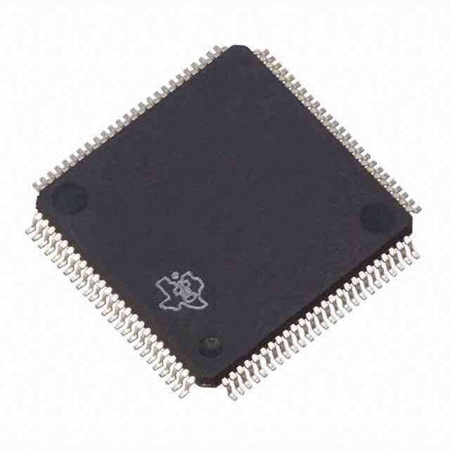
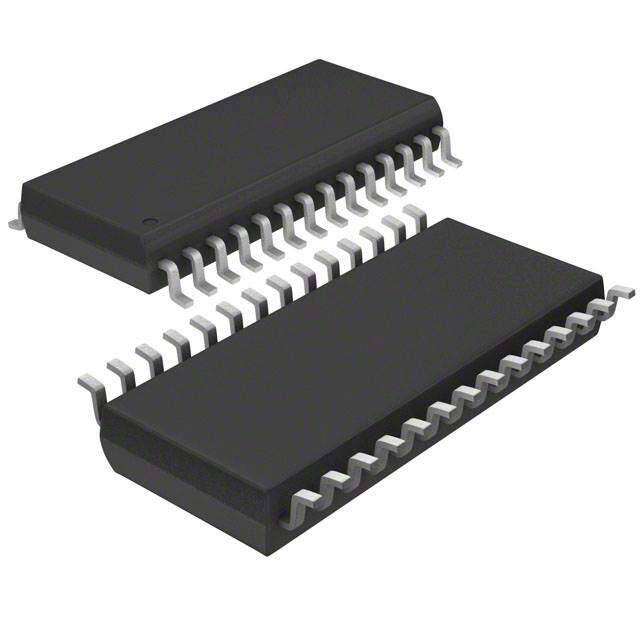
| 产品图片 |
|
| rohs | 符合RoHS无铅 / 符合限制有害物质指令(RoHS)规范要求 |
| 产品系列 | 嵌入式处理器和控制器,微控制器 - MCU,16位微控制器 - MCU,Texas Instruments MSP430G2231IN14MSP430G2xx |
| 数据手册 | 点击此处下载产品Datasheethttp://www.ti.com/lit/pdf/slau144 |
| 产品型号 | MSP430G2231IN14 |
| RAM容量 | 128 x 8 |
| 产品培训模块 | http://www.digikey.cn/PTM/IndividualPTM.page?site=cn&lang=zhs&ptm=8361http://www.digikey.cn/PTM/IndividualPTM.page?site=cn&lang=zhs&ptm=8522http://www.digikey.cn/PTM/IndividualPTM.page?site=cn&lang=zhs&ptm=8576http://www.digikey.cn/PTM/IndividualPTM.page?site=cn&lang=zhs&ptm=8679http://www.digikey.cn/PTM/IndividualPTM.page?site=cn&lang=zhs&ptm=24872http://www.digikey.cn/PTM/IndividualPTM.page?site=cn&lang=zhs&ptm=25404http://www.digikey.cn/PTM/IndividualPTM.page?site=cn&lang=zhs&ptm=25419http://www.digikey.cn/PTM/IndividualPTM.page?site=cn&lang=zhs&ptm=25427http://www.digikey.cn/PTM/IndividualPTM.page?site=cn&lang=zhs&ptm=25523http://www.digikey.cn/PTM/IndividualPTM.page?site=cn&lang=zhs&ptm=25524http://www.digikey.cn/PTM/IndividualPTM.page?site=cn&lang=zhs&ptm=25537http://www.digikey.cn/PTM/IndividualPTM.page?site=cn&lang=zhs&ptm=25788http://www.digikey.cn/PTM/IndividualPTM.page?site=cn&lang=zhs&ptm=25882http://www.digikey.cn/PTM/IndividualPTM.page?site=cn&lang=zhs&ptm=25885http://www.digikey.cn/PTM/IndividualPTM.page?site=cn&lang=zhs&ptm=26015http://www.digikey.cn/PTM/IndividualPTM.page?site=cn&lang=zhs&ptm=26006http://www.digikey.cn/PTM/IndividualPTM.page?site=cn&lang=zhs&ptm=30354 |
| 产品目录页面 | |
| 产品种类 | 16位微控制器 - MCU |
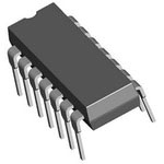
| 供应商器件封装 | 14-PDIP |
| 其它名称 | 296-25832-5 |
| 制造商产品页 | http://www.ti.com/general/docs/suppproductinfo.tsp?distId=10&orderablePartNumber=MSP430G2231IN14 |
| 包装 | 管件 |
| 可用A/D通道 | 8 Channel |
| 可编程输入/输出端数量 | 10 |
| 商标 | Texas Instruments |
| 商标名 | MSP430 |
| 处理器系列 | 2 Series |
| 外设 | 欠压检测/复位,POR,PWM,WDT |
| 安装风格 | Through Hole |
| 定时器数量 | 1 Timer |
| 封装 | Tube |
| 封装/外壳 | 14-DIP(0.300",7.62mm) |
| 封装/箱体 | PDIP-14 |
| 工作温度 | -40°C ~ 85°C |
| 工作电源电压 | 1.8 V to 3.6 V |
| 工厂包装数量 | 25 |
| 振荡器类型 | 内部 |
| 接口类型 | I2C, SPI |
| 数据RAM大小 | 128 B |
| 数据Ram类型 | SRAM |
| 数据总线宽度 | 16 bit |
| 数据转换器 | A/D 8x10b |
| 最大工作温度 | + 85 C |
| 最大时钟频率 | 16 MHz |
| 最小工作温度 | - 40 C |
| 标准包装 | 25 |
| 核心 | MSP430 |
| 核心处理器 | MSP430 |
| 核心尺寸 | 16-位 |
| 片上ADC | Yes |
| 特色产品 | http://www.digikey.com/cn/zh/ph/texas-instruments/msp430.html |
| 电压-电源(Vcc/Vdd) | 1.8 V ~ 3.6 V |
| 程序存储器大小 | 2 kB |
| 程序存储器类型 | 闪存 |
| 程序存储容量 | 2KB(2K x 8) |
| 系列 | MSP430G2231 |
| 视频文件 | http://www.digikey.cn/classic/video.aspx?PlayerID=1364138032001&width=640&height=455&videoID=1102983713001 |
| 输入/输出端数量 | 10 I/O |
| 连接性 | I²C, SPI |
| 速度 | 16MHz |
| 配用 | /product-detail/zh/MSP-EXP430G2/296-27570-ND/2331789 |


- 商务部:美国ITC正式对集成电路等产品启动337调查
- 曝三星4nm工艺存在良率问题 高通将骁龙8 Gen1或转产台积电
- 太阳诱电将投资9.5亿元在常州建新厂生产MLCC 预计2023年完工
- 英特尔发布欧洲新工厂建设计划 深化IDM 2.0 战略
- 台积电先进制程称霸业界 有大客户加持明年业绩稳了
- 达到5530亿美元!SIA预计今年全球半导体销售额将创下新高
- 英特尔拟将自动驾驶子公司Mobileye上市 估值或超500亿美元
- 三星加码芯片和SET,合并消费电子和移动部门,撤换高东真等 CEO
- 三星电子宣布重大人事变动 还合并消费电子和移动部门
- 海关总署:前11个月进口集成电路产品价值2.52万亿元 增长14.8%


PDF Datasheet 数据手册内容提取
MSP430G2x31 MSP430G2x21 www.ti.com SLAS694J–FEBRUARY2010–REVISEDFEBRUARY2013 MIXED SIGNAL MICROCONTROLLER FEATURES 1 • LowSupply-VoltageRange:1.8Vto3.6V • 16-BitTimer_AWithTwoCapture/Compare • Ultra-LowPowerConsumption Registers – ActiveMode:220µAat1MHz,2.2V • UniversalSerialInterface(USI)SupportingSPI andI2C(SeeTable1) – StandbyMode:0.5 µA • BrownoutDetector – OffMode(RAMRetention):0.1µA • 10-Bit200-kspsA/DConverterWithInternal • FivePower-SavingModes Reference,Sample-and-Hold,andAutoscan • Ultra-FastWake-UpFromStandbyModein (SeeTable1) LessThan1µs • SerialOnboardProgramming, • 16-BitRISCArchitecture,62.5-nsInstruction NoExternalProgrammingVoltageNeeded, CycleTime ProgrammableCodeProtectionbySecurity • BasicClockModuleConfigurations Fuse – InternalFrequenciesupto16MHzWith • On-ChipEmulationLogicWithSpy-Bi-Wire OneCalibratedFrequency Interface – InternalVeryLowPowerLow-Frequency • ForFamilyMembersDetails,SeeTable1 (LF)Oscillator • Availablein14-PinPlasticSmall-OutlineThin – 32-kHzCrystal Package(TSSOP)(PW),14-PinPlasticDual – ExternalDigitalClockSource InlinePackage(PDIP)(N),and16-PinQFN Package(RSA) • ForCompleteModuleDescriptions,Seethe MSP430x2xxFamilyUser’sGuide(SLAU144) DESCRIPTION The Texas Instruments MSP430 family of ultra-low-power microcontrollers consists of several devices featuring different sets of peripherals targeted for various applications. The architecture, combined with five low-power modes,isoptimizedtoachieveextendedbatterylifeinportablemeasurementapplications.Thedevicefeaturesa powerful 16-bit RISC CPU, 16-bit registers, and constant generators that contribute to maximum code efficiency. Thedigitallycontrolledoscillator(DCO)allowswake-upfromlow-powermodestoactivemodeinlessthan1µs. The MSP430G2x21/G2x31 series is an ultra-low-power mixed signal microcontroller with a built-in 16-bit timer and ten I/O pins. The MSP430G2x31 family members have a 10-bit A/D converter and built-in communication capabilityusingsynchronousprotocols(SPIorI2C).Forconfigurationdetails,seeTable1. Typical applications include low-cost sensor systems that capture analog signals, convert them to digital values, andthenprocessthedatafordisplayorfortransmissiontoahostsystem. 1 Pleasebeawarethatanimportantnoticeconcerningavailability,standardwarranty,anduseincriticalapplicationsof TexasInstrumentssemiconductorproductsanddisclaimerstheretoappearsattheendofthisdatasheet. PRODUCTIONDATAinformationiscurrentasofpublicationdate. Copyright©2010–2013,TexasInstrumentsIncorporated Products conform to specifications per the terms of the Texas Instruments standard warranty. Production processing does not necessarilyincludetestingofallparameters.
MSP430G2x31 MSP430G2x21 SLAS694J–FEBRUARY2010–REVISEDFEBRUARY2013 www.ti.com Table1.AvailableOptions(1) Flash RAM ADC10 Package Device BSL EEM (KB) (B) Timer_A USI Channel Clock I/O Type(2) MSP430G2231IRSA16 16-QFN MSP430G2231IPW14 - 1 2 128 1xTA2 1 8 LF,DCO,VLO 10 14-TSSOP MSP430G2231IN14 14-PDIP MSP430G2221IRSA16 16-QFN MSP430G2221IPW14 - 1 2 128 1xTA2 1 - LF,DCO,VLO 10 14-TSSOP MSP430G2221IN14 14-PDIP MSP430G2131IRSA16 16-QFN MSP430G2131IPW14 - 1 1 128 1xTA2 1 8 LF,DCO,VLO 10 14-TSSOP MSP430G2131IN14 14-PDIP MSP430G2121IRSA16 16-QFN MSP430G2121IPW14 - 1 1 128 1xTA2 1 - LF,DCO,VLO 10 14-TSSOP MSP430G2121IN14 14-PDIP (1) Forthemostcurrentpackageandorderinginformation,seethePackageOptionAddendumattheendofthisdocument,orseetheTI websiteatwww.ti.com. (2) Packagedrawings,thermaldata,andsymbolizationareavailableatwww.ti.com/packaging. 2 SubmitDocumentationFeedback Copyright©2010–2013,TexasInstrumentsIncorporated
MSP430G2x31 MSP430G2x21 www.ti.com SLAS694J–FEBRUARY2010–REVISEDFEBRUARY2013 Device Pinout, MSP430G2x21 NORPWPACKAGE (TOPVIEW) DVCC 1 14 DVSS P1.0/TA0CLK/ACLK 2 13 XIN/P2.6/TA0.1 P1.1/TA0.0 3 12 XOUT/P2.7 P1.2/TA0.1 4 11 TEST/SBWTCK P1.3 5 10 RST/NMI/SBWTDIO P1.4/SMCLK/TCK 6 9 P1.7/SDI/SDA/TDO/TDI P1.5/TA0.0/SCLK/TMS 7 8 P1.6/TA0.1/SDO/SCL/TDI/TCLK NOTE: SeeportschematicsinApplicationInformationfordetailedI/Oinformation. RSAPACKAGE (TOPVIEW) C C S S C C S S V V V V D D D D 16 15 14 13 P1.0/TA0CLK/ACLK 1 12 XIN/P2.6/TA0.1 P1.1/TA0.0 2 11 XOUT/P2.7 P1.2/TA0.1 3 10 TEST/SBWTCK P1.3 4 9 RST/NMI/SBWTDIO 5 6 7 8 K S K DI C M L T CLK/T CLK/T DI/TC TDO/ P1.4/SM P1.5/TA0.0/S 1/SDO/SCL/T 1.7/SDI/SDA/ 0. P A T 6/ 1. P NOTE: SeeportschematicsinApplicationInformationfordetailedI/Oinformation. Copyright©2010–2013,TexasInstrumentsIncorporated SubmitDocumentationFeedback 3
MSP430G2x31 MSP430G2x21 SLAS694J–FEBRUARY2010–REVISEDFEBRUARY2013 www.ti.com Device Pinout, MSP430G2x31 NORPWPACKAGE (TOPVIEW) DVCC 1 14 DVSS P1.0/TA0CLK/ACLK/A0 2 13 XIN/P2.6/TA0.1 P1.1/TA0.0/A1 3 12 XOUT/P2.7 P1.2/TA0.1/A2 4 11 TEST/SBWTCK P1.3/ADC10CLK/A3/VREF-/VEREF- 5 10 RST/NMI/SBWTDIO P1.4/SMCLK/A4/VREF+/VEREF+/TCK 6 9 P1.7/A7/SDI/SDA/TDO/TDI P1.5/TA0.0/A5/SCLK/TMS 7 8 P1.6/TA0.1/A6/SDO/SCL/TDI/TCLK NOTE: SeeportschematicsinApplicationInformationfordetailedI/Oinformation. RSAPACKAGE (TOPVIEW) C C S S C C S S V V V V D D D D 16 15 14 13 P1.0/TA0CLK/ACLK/A0 1 12 XIN/P2.6/TA0.1 P1.1/TA0.0/A1 2 11 XOUT/P2.7 P1.2/TA0.1/A2 3 10 TEST/SBWTCK P1.3/ADC10CLK/A3/VREF-/VEREF- 4 9 RST/NMI/SBWTDIO 5 6 7 8 F+/VEREF+/TCK 0/SCLK/A5/TMS O/SCL/TDI/TCLK DI/SDA/TDO/TDI E 0. D S K/A4/VR P1.5/TA TA0.1/S P1.7/ L 6/ MC P1. S 4/ 1. P NOTE: SeeportschematicsinApplicationInformationfordetailedI/Oinformation. 4 SubmitDocumentationFeedback Copyright©2010–2013,TexasInstrumentsIncorporated
MSP430G2x31 MSP430G2x21 www.ti.com SLAS694J–FEBRUARY2010–REVISEDFEBRUARY2013 FunctionalBlockDiagram,MSP430G2x21 XIN XOUT DVCC DVSS P1.x P2.x 8 2 ACLK PortP1 PortP2 Clock System SMCLK Flash RAM 8I/O 2I/O Interrupt Interrupt 2KB 128B capability capability MCLK 1KB pull-up/down pull-up/down resistors resistors 16MHz MAB CPU incl.16 Registers MDB Emulation USI 2BP Watchdog Timer0_A2 Brownout WDT+ Universal JTAG Protection 2CC Serial Interface 15-Bit Registers Interface SPI,I2C Spy-Bi Wire RST/NMI FunctionalBlockDiagram,MSP430G2x31 XIN XOUT DVCC DVSS P1.x P2.x 8 2 ACLK PortP1 PortP2 Clock ADC System SMCLK Flash RAM 8I/O 2I/O 10-Bit Interrupt Interrupt 2kB 8Ch. 128B capability capability MCLK 1kB Autoscan pull-up/down pull-up/down 1chDMA resistors resistors 16MHz MAB CPU incl.16 Registers MDB Emulation USI 2BP Watchdog Timer0_A2 Brownout WDT+ Universal JTAG Protection 2CC Serial Interface 15-Bit Registers Interface SPI,I2C Spy-Bi Wire RST/NMI Copyright©2010–2013,TexasInstrumentsIncorporated SubmitDocumentationFeedback 5
MSP430G2x31 MSP430G2x21 SLAS694J–FEBRUARY2010–REVISEDFEBRUARY2013 www.ti.com Table2.TerminalFunctions TERMINAL NO. I/O DESCRIPTION NAME N,PW RSA P1.0/ General-purposedigitalI/Opin TA0CLK/ Timer0_A,clocksignalTACLKinput 2 1 I/O ACLK/ ACLKsignaloutput A0 ADC10analoginputA0(1) P1.1/ General-purposedigitalI/Opin TA0.0/ 3 2 I/O Timer0_A,capture:CCI0Ainput,compare:Out0output A1 ADC10analoginputA1(1) P1.2/ General-purposedigitalI/Opin TA0.1/ 4 3 I/O Timer0_A,capture:CCI1Ainput,compare:Out1output A2 ADC10analoginputA2(1) P1.3/ General-purposedigitalI/Opin ADC10CLK/ ADC10,conversionclockoutput(1) A3/ 5 4 I/O ADC10analoginputA3(1) VREF-/VEREF ADC10negativereferencevoltage(1) P1.4/ General-purposedigitalI/Opin SMCLK/ SMCLKsignaloutput A4/ 6 5 I/O ADC10analoginputA4(1) VREF+/VEREF+/ ADC10positivereferencevoltage(1) TCK JTAGtestclock,inputterminalfordeviceprogrammingandtest P1.5/ General-purposedigitalI/Opin TA0.0/ Timer0_A,compare:Out0output A5/ 7 6 I/O ADC10analoginputA5(1) SCLK/ USI:clockinputinI2Cmode;clockinput/outputinSPImode TMS JTAGtestmodeselect,inputterminalfordeviceprogrammingandtest P1.6/ General-purposedigitalI/Opin TA0.1/ Timer0_A,capture:CCI1Ainput,compare:Out1output A6/ ADC10analoginputA6(1) 8 7 I/O SDO/ USI:DataoutputinSPImode SCL/ USI:I2CclockinI2Cmode TDI/TCLK JTAGtestdatainputortestclockinputduringprogrammingandtest P1.7/ General-purposedigitalI/Opin A7/ ADC10analoginputA7(1) SDI/ 9 8 I/O USI:DatainputinSPImode SDA/ USI:I2CdatainI2Cmode TDO/TDI(2) JTAGtestdataoutputterminalortestdatainputduringprogrammingandtest XIN/ Inputterminalofcrystaloscillator P2.6/ 13 12 I/O General-purposedigitalI/Opin TA0.1 Timer0_A,compare:Out1output XOUT/ Outputterminalofcrystaloscillator(3) 12 11 I/O P2.7 General-purposedigitalI/Opin RST/ Reset NMI/ 10 9 I Nonmaskableinterruptinput SBWTDIO Spy-Bi-Wiretestdatainput/outputduringprogrammingandtest TEST/ SelectstestmodeforJTAGpinsonPort1.ThedeviceprotectionfuseisconnectedtoTEST. 11 10 I SBWTCK Spy-Bi-Wiretestclockinputduringprogrammingandtest DVCC 1 15,16 NA Supplyvoltage DVSS 14 13,14 NA Groundreference QFNPad - Pad NA QFNpackagepadconnectiontoV recommended. SS (1) MSP430G2x31only (2) TDOorTDIisselectedviaJTAGinstruction. (3) IfXOUT/P2.7isusedasaninput,excesscurrentwillflowuntilP2SEL.7iscleared.Thisisduetotheoscillatoroutputdriverconnection tothispadafterreset. 6 SubmitDocumentationFeedback Copyright©2010–2013,TexasInstrumentsIncorporated
MSP430G2x31 MSP430G2x21 www.ti.com SLAS694J–FEBRUARY2010–REVISEDFEBRUARY2013 SHORT-FORM DESCRIPTION CPU The MSP430 CPU has a 16-bit RISC architecture that is highly transparent to the application. All Program Counter PC/R0 operations, other than program-flow instructions, are performed as register operations in conjunction with Stack Pointer SP/R1 seven addressing modes for source operand and four Status Register SR/CG1/R2 addressingmodesfordestinationoperand. The CPU is integrated with 16 registers that provide Constant Generator CG2/R3 reduced instruction execution time. The register-to- General-Purpose Register R4 register operation execution time is one cycle of the CPUclock. General-Purpose Register R5 Four of the registers, R0 to R3, are dedicated as General-Purpose Register R6 program counter, stack pointer, status register, and constant generator, respectively. The remaining General-Purpose Register R7 registersaregeneral-purposeregisters. General-Purpose Register R8 Peripherals are connected to the CPU using data, address, and control buses, and can be handled with General-Purpose Register R9 allinstructions. General-Purpose Register R10 The instruction set consists of the original 51 instructions with three formats and seven address General-Purpose Register R11 modes and additional instructions for the expanded address range. Each instruction can operate on word General-Purpose Register R12 andbytedata. General-Purpose Register R13 Instruction Set General-Purpose Register R14 The instruction set consists of 51 instructions with General-Purpose Register R15 three formats and seven address modes. Each instruction can operate on word and byte data. Table 3 shows examples of the three types of instruction formats; Table 4 shows the address modes. Table3.InstructionWordFormats INSTRUCTIONFORMAT SYNTAX OPERATION Dualoperands,source-destination ADDR4,R5 R4+R5--->R5 Singleoperands,destinationonly CALLR8 PC-->(TOS),R8-->PC Relativejump,un/conditional JNE Jump-on-equalbit=0 Table4.AddressModeDescriptions(1) ADDRESSMODE S D SYNTAX EXAMPLE OPERATION Register ✓ ✓ MOVRs,Rd MOVR10,R11 R10---->R11 Indexed ✓ ✓ MOVX(Rn),Y(Rm) MOV2(R5),6(R6) M(2+R5)---->M(6+R6) Symbolic(PCrelative) ✓ ✓ MOVEDE,TONI M(EDE)---->M(TONI) Absolute ✓ ✓ MOV&MEM,&TCDAT M(MEM)---->M(TCDAT) Indirect ✓ MOV@Rn,Y(Rm) MOV@R10,Tab(R6) M(R10)---->M(Tab+R6) M(R10)---->R11 Indirectautoincrement ✓ MOV@Rn+,Rm MOV@R10+,R11 R10+2---->R10 Immediate ✓ MOV#X,TONI MOV#45,TONI #45---->M(TONI) (1) S=source,D=destination Copyright©2010–2013,TexasInstrumentsIncorporated SubmitDocumentationFeedback 7
MSP430G2x31 MSP430G2x21 SLAS694J–FEBRUARY2010–REVISEDFEBRUARY2013 www.ti.com Operating Modes The MSP430 has one active mode and five software selectable low-power modes of operation. An interrupt event can wake up the device from any of the low-power modes, service the request, and restore back to the low-powermodeonreturnfromtheinterruptprogram. Thefollowingsixoperatingmodescanbeconfiguredbysoftware: • Activemode(AM) – Allclocksareactive • Low-powermode0(LPM0) – CPUisdisabled – ACLKandSMCLKremainactive,MCLKisdisabled • Low-powermode1(LPM1) – CPUisdisabled – ACLKandSMCLKremainactive,MCLKisdisabled – DCO'sdcgeneratorisdisabledifDCOnotusedinactivemode • Low-powermode2(LPM2) – CPUisdisabled – MCLKandSMCLKaredisabled – DCO'sdcgeneratorremainsenabled – ACLKremainsactive • Low-powermode3(LPM3) – CPUisdisabled – MCLKandSMCLKaredisabled – DCO'sdcgeneratorisdisabled – ACLKremainsactive • Low-powermode4(LPM4) – CPUisdisabled – ACLKisdisabled – MCLKandSMCLKaredisabled – DCO'sdcgeneratorisdisabled – Crystaloscillatorisstopped 8 SubmitDocumentationFeedback Copyright©2010–2013,TexasInstrumentsIncorporated
MSP430G2x31 MSP430G2x21 www.ti.com SLAS694J–FEBRUARY2010–REVISEDFEBRUARY2013 Interrupt Vector Addresses The interrupt vectors and the power-up starting address are located in the address range 0FFFFh to 0FFC0h. Thevectorcontainsthe16-bitaddressoftheappropriateinterrupthandlerinstructionsequence. If the reset vector (located at address 0FFFEh) contains 0FFFFh (for example, flash is not programmed) the CPUgoesintoLPM4immediatelyafterpower-up. Table5.InterruptSources,Flags,andVectors SYSTEM WORD INTERRUPTSOURCE INTERRUPTFLAG PRIORITY INTERRUPT ADDRESS Power-Up PORIFG ExternalReset RSTIFG WatchdogTimer+ WDTIFG Reset 0FFFEh 31,highest Flashkeyviolation KEYV(2) PCout-of-range(1) NMI NMIIFG (non)-maskable Oscillatorfault OFIFG (non)-maskable 0FFFCh 30 Flashmemoryaccessviolation ACCVIFG(2)(3) (non)-maskable 0FFFAh 29 0FFF8h 28 0FFF6h 27 WatchdogTimer+ WDTIFG maskable 0FFF4h 26 Timer_A2 TACCR0CCIFG(4) maskable 0FFF2h 25 Timer_A2 TACCR1CCIFG,TAIFG(2)(4) maskable 0FFF0h 24 0FFEEh 23 0FFECh 22 ADC10(5) ADC10IFG(4)(5) maskable 0FFEAh 21 USI USIIFG,USISTTIFG(2)(4) maskable 0FFE8h 20 I/OPortP2(twoflags) P2IFG.6toP2IFG.7(2)(4) maskable 0FFE6h 19 I/OPortP1(eightflags) P1IFG.0toP1IFG.7(2)(4) maskable 0FFE4h 18 0FFE2h 17 0FFE0h 16 See (6) 0FFDEhto 15to0,lowest 0FFC0h (1) AresetisgeneratediftheCPUtriestofetchinstructionsfromwithinthemoduleregistermemoryaddressrange(0hto01FFh)orfrom withinunusedaddressranges. (2) Multiplesourceflags (3) (non)-maskable:theindividualinterrupt-enablebitcandisableaninterruptevent,butthegeneralinterruptenablecannot. (4) Interruptflagsarelocatedinthemodule. (5) MSP430G2x31only (6) Theinterruptvectorsataddresses0FFDEhto0FFC0harenotusedinthisdeviceandcanbeusedforregularprogramcodeif necessary. Copyright©2010–2013,TexasInstrumentsIncorporated SubmitDocumentationFeedback 9
MSP430G2x31 MSP430G2x21 SLAS694J–FEBRUARY2010–REVISEDFEBRUARY2013 www.ti.com Special Function Registers (SFRs) Most interrupt and module enable bits are collected into the lowest address space. Special function register bits not allocated to a functional purpose are not physically present in the device. Simple software access is provided withthisarrangement. Legend rw: Bitcanbereadandwritten. rw-0,1: Bitcanbereadandwritten.ItisresetorsetbyPUC. rw-(0,1): Bitcanbereadandwritten.ItisresetorsetbyPOR. SFRbitisnotpresentindevice. Table6.InterruptEnableRegister1and2 Address 7 6 5 4 3 2 1 0 00h ACCVIE NMIIE OFIE WDTIE rw-0 rw-0 rw-0 rw-0 WDTIE WatchdogTimerinterruptenable.Inactiveifwatchdogmodeisselected.ActiveifWatchdogTimerisconfiguredin intervaltimermode. OFIE Oscillatorfaultinterruptenable NMIIE (Non)maskableinterruptenable ACCVIE Flashaccessviolationinterruptenable Address 7 6 5 4 3 2 1 0 01h Table7.InterruptFlagRegister1and2 Address 7 6 5 4 3 2 1 0 02h NMIIFG RSTIFG PORIFG OFIFG WDTIFG rw-0 rw-(0) rw-(1) rw-1 rw-(0) WDTIFG Setonwatchdogtimeroverflow(inwatchdogmode)orsecuritykeyviolation. ResetonV power-onoraresetconditionattheRST/NMIpininresetmode. CC OFIFG Flagsetonoscillatorfault. PORIFG Power-OnResetinterruptflag.SetonV power-up. CC RSTIFG Externalresetinterruptflag.SetonaresetconditionatRST/NMIpininresetmode.ResetonV power-up. CC NMIIFG SetviaRST/NMIpin Address 7 6 5 4 3 2 1 0 03h 10 SubmitDocumentationFeedback Copyright©2010–2013,TexasInstrumentsIncorporated
MSP430G2x31 MSP430G2x21 www.ti.com SLAS694J–FEBRUARY2010–REVISEDFEBRUARY2013 Memory Organization Table8.MemoryOrganization MSP430G2021 MSP430G2121 MSP430G2221 MSP430G2031 MSP430G2131 MSP430G2231 Memory Size 512B 1kB 2kB Main:interruptvector Flash 0xFFFFto0xFFC0 0xFFFFto0xFFC0 0xFFFFto0xFFC0 Main:codememory Flash 0xFFFFto0xFE00 0xFFFFto0xFC00 0xFFFFto0xF800 Informationmemory Size 256Byte 256Byte 256Byte Flash 010FFhto01000h 010FFhto01000h 010FFhto01000h RAM Size 128B 128B 128B 027Fhto0200h 027Fhto0200h 027Fhto0200h Peripherals 16-bit 01FFhto0100h 01FFhto0100h 01FFhto0100h 8-bit 0FFhto010h 0FFhto010h 0FFhto010h 8-bitSFR 0Fhto00h 0Fhto00h 0Fhto00h Flash Memory The flash memory can be programmed via the Spy-Bi-Wire/JTAG port or in-system by the CPU. The CPU can performsingle-byteandsingle-wordwritestotheflashmemory.Featuresoftheflashmemoryinclude: • Flash memory has n segments of main memory and four segments of information memory (A to D) of 64byteseach.Eachsegmentinmainmemoryis512bytesinsize. • Segments0tonmaybeerasedinonestep,oreachsegmentmaybeindividuallyerased. • Segments A to D can be erased individually or as a group with segments 0 to n. Segments A to D are also calledinformationmemory. • Segment A contains calibration data. After reset segment A is protected against programming and erasing. It can be unlocked but care should be taken not to erase this segment if the device-specific calibration data is required. Copyright©2010–2013,TexasInstrumentsIncorporated SubmitDocumentationFeedback 11
MSP430G2x31 MSP430G2x21 SLAS694J–FEBRUARY2010–REVISEDFEBRUARY2013 www.ti.com Peripherals Peripherals are connected to the CPU through data, address, and control buses and can be handled using all instructions.Forcompletemoduledescriptions,seetheMSP430x2xxFamilyUser'sGuide(SLAU144). OscillatorandSystemClock The clock system is supported by the basic clock module that includes support for a 32768-Hz watch crystal oscillator, an internal very-low-power low-frequency oscillator and an internal digitally controlled oscillator (DCO). The basic clock module is designed to meet the requirements of both low system cost and low power consumption. The internal DCO provides a fast turn-on clock source and stabilizes in less than 1µs. The basic clockmoduleprovidesthefollowingclocksignals: • Auxiliaryclock(ACLK),sourcedeitherfroma32768-HzwatchcrystalortheinternalLFoscillator. • Mainclock(MCLK),thesystemclockusedbytheCPU. • Sub-Mainclock(SMCLK),thesub-systemclockusedbytheperipheralmodules. Table9.DCOCalibrationData (ProvidedFromFactoryInFlashInformationMemorySegmentA) CALIBRATION DCOFREQUENCY SIZE ADDRESS REGISTER CALBC1_1MHZ byte 010FFh 1MHz CALDCO_1MHZ byte 010FEh Brownout The brownout circuit is implemented to provide the proper internal reset signal to the device during power on and poweroff. DigitalI/O Thereisone8-bitI/Oportimplemented—portP1—andtwobitsofI/OportP2: • AllindividualI/Obitsareindependentlyprogrammable. • Anycombinationofinput,output,andinterruptconditionispossible. • Edge-selectableinterruptinputcapabilityforalltheeightbitsofportP1andthetwobitsofportP2. • Read/writeaccesstoport-controlregistersissupportedbyallinstructions. • EachI/Ohasanindividuallyprogrammablepull-up/pull-downresistor. WDT+WatchdogTimer The primary function of the watchdog timer (WDT+) module is to perform a controlled system restart after a software problem occurs. If the selected time interval expires, a system reset is generated. If the watchdog function is not needed in an application, the module can be disabled or configured as an interval timer and can generateinterruptsatselectedtimeintervals. 12 SubmitDocumentationFeedback Copyright©2010–2013,TexasInstrumentsIncorporated
MSP430G2x31 MSP430G2x21 www.ti.com SLAS694J–FEBRUARY2010–REVISEDFEBRUARY2013 Timer_A2 Timer_A2 is a 16-bit timer/counter with two capture/compare registers. Timer_A2 can support multiple capture/compares, PWM outputs, and interval timing. Timer_A2 also has extensive interrupt capabilities. Interrupts may be generated from the counter on overflow conditions and from each of the capture/compare registers. Table10.Timer_A2SignalConnections– DeviceWithADC10 INPUTPINNUMBER MODULE OUTPUTPINNUMBER DEVICEINPUT MODULE MODULE OUTPUT PW,N RSA SIGNAL INPUTNAME BLOCK SIGNAL PW,N RSA 2-P1.0 1-P1.0 TACLK TACLK ACLK ACLK Timer NA SMCLK SMCLK 2-P1.0 1-P1.0 TACLK INCLK 3-P1.1 2-P1.1 TA0 CCI0A 3-P1.1 2-P1.1 ACLK(internal) CCI0B 7-P1.5 6-P1.5 CCR0 TA0 VSS GND VCC VCC 4-P1.2 3-P1.2 TA1 CCI1A 4-P1.2 3-P1.2 8-P1.6 7-P1.6 TA1 CCI1B 8-P1.6 7-P1.6 CCR1 TA1 VSS GND 13-P2.6 12-P2.6 VCC VCC USI The universal serial interface (USI) module is used for serial data communication and provides the basic hardwareforsynchronouscommunicationprotocolslikeSPIandI2C. ADC10(MSP430G2x31only) The ADC10 module supports fast, 10-bit analog-to-digital conversions. The module implements a 10-bit SAR core, sample select control, reference generator and data transfer controller, or DTC, for automatic conversion resulthandling,allowingADCsamplestobeconvertedandstoredwithoutanyCPUintervention. Copyright©2010–2013,TexasInstrumentsIncorporated SubmitDocumentationFeedback 13
MSP430G2x31 MSP430G2x21 SLAS694J–FEBRUARY2010–REVISEDFEBRUARY2013 www.ti.com PeripheralFileMap Table11.PeripheralsWithWordAccess REGISTER MODULE REGISTERDESCRIPTION OFFSET NAME ADC10(MSP430G2x31only) ADCdatatransferstartaddress ADC10SA 1BCh ADCcontrol0 ADC10CTL0 01B0h ADCcontrol1 ADC10CTL0 01B2h ADCmemory ADC10MEM 01B4h Timer_A Capture/compareregister TACCR1 0174h Capture/compareregister TACCR0 0172h Timer_Aregister TAR 0170h Capture/comparecontrol TACCTL1 0164h Capture/comparecontrol TACCTL0 0162h Timer_Acontrol TACTL 0160h Timer_Ainterruptvector TAIV 012Eh FlashMemory Flashcontrol3 FCTL3 012Ch Flashcontrol2 FCTL2 012Ah Flashcontrol1 FCTL1 0128h WatchdogTimer+ Watchdog/timercontrol WDTCTL 0120h Table12.PeripheralsWithByteAccess REGISTER MODULE REGISTERDESCRIPTION OFFSET NAME ADC10(MSP430G2x31only) ADCanalogenable ADC10AE0 04Ah ADCdatatransfercontrol1 ADC10DTC1 049h ADCdatatransfercontrol0 ADC10DTC0 048h USI USIcontrol0 USICTL0 078h USIcontrol1 USICTL1 079h USIclockcontrol USICKCTL 07Ah USIbitcounter USICNT 07Bh USIshiftregister USISR 07Ch BasicClockSystem+ Basicclocksystemcontrol3 BCSCTL3 053h Basicclocksystemcontrol2 BCSCTL2 058h Basicclocksystemcontrol1 BCSCTL1 057h DCOclockfrequencycontrol DCOCTL 056h PortP2 PortP2resistorenable P2REN 02Fh PortP2selection P2SEL 02Eh PortP2interruptenable P2IE 02Dh PortP2interruptedgeselect P2IES 02Ch PortP2interruptflag P2IFG 02Bh PortP2direction P2DIR 02Ah PortP2output P2OUT 029h PortP2input P2IN 028h 14 SubmitDocumentationFeedback Copyright©2010–2013,TexasInstrumentsIncorporated
MSP430G2x31 MSP430G2x21 www.ti.com SLAS694J–FEBRUARY2010–REVISEDFEBRUARY2013 Table12.PeripheralsWithByteAccess(continued) REGISTER MODULE REGISTERDESCRIPTION OFFSET NAME PortP1 PortP1resistorenable P1REN 027h PortP1selection P1SEL 026h PortP1interruptenable P1IE 025h PortP1interruptedgeselect P1IES 024h PortP1interruptflag P1IFG 023h PortP1direction P1DIR 022h PortP1output P1OUT 021h PortP1input P1IN 020h SpecialFunction SFRinterruptflag2 IFG2 003h SFRinterruptflag1 IFG1 002h SFRinterruptenable2 IE2 001h SFRinterruptenable1 IE1 000h Copyright©2010–2013,TexasInstrumentsIncorporated SubmitDocumentationFeedback 15
MSP430G2x31 MSP430G2x21 SLAS694J–FEBRUARY2010–REVISEDFEBRUARY2013 www.ti.com Absolute Maximum Ratings(1) VoltageappliedatV toV –0.3Vto4.1V CC SS Voltageappliedtoanypin(2) –0.3VtoV +0.3V CC Diodecurrentatanydevicepin ±2mA Unprogrammeddevice –55°Cto150°C Storagetemperaturerange,T (3) stg Programmeddevice –55°Cto150°C (1) Stressesbeyondthoselistedunder"absolutemaximumratings"maycausepermanentdamagetothedevice.Thesearestressratings only,andfunctionaloperationofthedeviceattheseoranyotherconditionsbeyondthoseindicatedunder"recommendedoperating conditions"isnotimplied.Exposuretoabsolute-maximum-ratedconditionsforextendedperiodsmayaffectdevicereliability. (2) AllvoltagesreferencedtoV .TheJTAGfuse-blowvoltage,V ,isallowedtoexceedtheabsolutemaximumrating.Thevoltageis SS FB appliedtotheTESTpinwhenblowingtheJTAGfuse. (3) HighertemperaturemaybeappliedduringboardsolderingaccordingtothecurrentJEDECJ-STD-020specificationwithpeakreflow temperaturesnothigherthanclassifiedonthedevicelabelontheshippingboxesorreels. Recommended Operating Conditions TypicalvaluesarespecifiedatV =3.3VandT =25°C(unlessotherwisenoted) CC A MIN NOM MAX UNIT Duringprogramexecution 1.8 3.6 V Supplyvoltage V CC Duringflashprogramming 2.2 3.6 V Supplyvoltage 0 V SS T Operatingfree-airtemperature Iversion –40 85 °C A V =1.8V, CC dc 6 Dutycycle=50%±10% f Processorfrequency(maximumMCLKfrequency)(1)(2) VCC=2.7V, dc 12 MHz SYSTEM Dutycycle=50%±10% V =3.3V, CC dc 16 Dutycycle=50%±10% (1) TheMSP430CPUisclockeddirectlywithMCLK.BoththehighandlowphaseofMCLKmustnotexceedthepulsewidthofthe specifiedmaximumfrequency. (2) Modulesmighthaveadifferentmaximuminputclockspecification.Seethespecificationoftherespectivemoduleinthisdatasheet. Legend: 16 MHz Supply voltage range, Hz during flash memory M programming y - 12 MHz c n e u Supply voltage range, q e during program execution Fr m ste 6 MHz y S 1.8 V 2.2 V 2.7 V 3.3 V 3.6 V Supply Voltage - V Note: Minimumprocessorfrequencyisdefinedbysystemclock.FlashprogramoreraseoperationsrequireaminimumV CC of2.2V. Figure1. SafeOperatingArea 16 SubmitDocumentationFeedback Copyright©2010–2013,TexasInstrumentsIncorporated
MSP430G2x31 MSP430G2x21 www.ti.com SLAS694J–FEBRUARY2010–REVISEDFEBRUARY2013 Electrical Characteristics Active Mode Supply Current Into V Excluding External Current CC overrecommendedrangesofsupplyvoltageandoperatingfree-airtemperature(unlessotherwisenoted)(1)(2) PARAMETER TESTCONDITIONS T V MIN TYP MAX UNIT A CC f =f =f =1MHz, 2.2V 220 DCO MCLK SMCLK f =32768Hz, ACLK Programexecutesinflash, Activemode(AM) I BCSCTL1=CALBC1_1MHZ, µA AM,1MHz current(1MHz) DCOCTL=CALDCO_1MHZ, 3V 300 370 CPUOFF=0,SCG0=0,SCG1=0, OSCOFF=0 (1) Allinputsaretiedto0VortoV .Outputsdonotsourceorsinkanycurrent. CC (2) ThecurrentsarecharacterizedwithaMicroCrystalCC4V-T1ASMDcrystalwithaloadcapacitanceof9pF.Theinternalandexternal loadcapacitanceischosentocloselymatchtherequired9pF. Typical Characteristics – Active Mode Supply Current (Into V ) CC 5.0 4.0 4.0 fDCO= 16 MHz TA= 85°C A A 3.0 m m − − TA= 25°C Active Mode Current 23..00 fDCO= 8 MfHDzCO= 12 MHz Active Mode Current 12..00 VCC= 3 V TTAA== 8255°°CC 1.0 fDCO= 1 MHz VCC= 2.2 V 0.0 0.0 1.5 2.0 2.5 3.0 3.5 4.0 0.0 4.0 8.0 12.0 16.0 VCC−Supply Voltage−V fDCO−DCO Frequency−MHz Figure2.ActiveModeCurrentvsV ,T =25°C Figure3.ActiveModeCurrentvsDCOFrequency CC A Copyright©2010–2013,TexasInstrumentsIncorporated SubmitDocumentationFeedback 17
MSP430G2x31 MSP430G2x21 SLAS694J–FEBRUARY2010–REVISEDFEBRUARY2013 www.ti.com Low-Power Mode Supply Currents (Into V ) Excluding External Current CC overrecommendedrangesofsupplyvoltageandoperatingfree-airtemperature(unlessotherwisenoted)(1) (2) PARAMETER TESTCONDITIONS T V MIN TYP MAX UNIT A CC f =0MHz, MCLK f =f =1MHz, SMCLK DCO f =32768Hz, Low-powermode0 ACLK ILPM0,1MHz (LPM0)current(3) BCSCTL1=CALBC1_1MHZ, 25°C 2.2V 65 µA DCOCTL=CALDCO_1MHZ, CPUOFF=1,SCG0=0,SCG1=0, OSCOFF=0 f =f =0MHz, MCLK SMCLK f =1MHz, DCO f =32768Hz, Low-powermode2 ACLK ILPM2 (LPM2)current(4) BCSCTL1=CALBC1_1MHZ, 25°C 2.2V 22 µA DCOCTL=CALDCO_1MHZ, CPUOFF=1,SCG0=0,SCG1=1, OSCOFF=0 f =f =f =0MHz, DCO MCLK SMCLK Low-powermode3 f =32768Hz, ILPM3,LFXT1 (LPM3)current(4) CAPCLUKOFF=1,SCG0=1,SCG1=1, 25°C 2.2V 0.7 1.5 µA OSCOFF=0 f =f =f =0MHz, DCO MCLK SMCLK Low-powermode3 f frominternalLFoscillator(VLO), ILPM3,VLO current,(LPM3)(4) CAPCLUKOFF=1,SCG0=1,SCG1=1, 25°C 2.2V 0.5 0.7 µA OSCOFF=0 f =f =f =0MHz, 25°C 2.2V 0.1 0.5 µA DCO MCLK SMCLK Low-powermode4 f =0Hz, ILPM4 (LPM4)current(5) CAPCLUKOFF=1,SCG0=1,SCG1=1, 85°C 2.2V 0.8 1.5 µA OSCOFF=1 (1) Allinputsaretiedto0VortoV .Outputsdonotsourceorsinkanycurrent. CC (2) ThecurrentsarecharacterizedwithaMicroCrystalCC4V-T1ASMDcrystalwithaloadcapacitanceof9pF. (3) CurrentforbrownoutandWDTclockedbySMCLKincluded. (4) CurrentforbrownoutandWDTclockedbyACLKincluded. (5) Currentforbrownoutincluded. Typical Characteristics Low-Power Mode Supply Currents overrecommendedrangesofsupplyvoltageandoperatingfree-airtemperature(unlessotherwisenoted) 3.00 2.50 2.75 2.25 A A µ 2.50 µ – – 2.00 Current 22..0205 Current 1.75 w-Power Mode 1111....02570505 VVcccc = = 3 3.6 V V w-Power Mode 111...025050 VVcccc = = 3 3.6 V V –Lo 0.75 Vcc = 2.2 V –Lo 0.75 Vcc = 2.2 V ILPM3 0.50 Vcc = 1.8 V ILPM4 00..2550 0.25 Vcc = 1.8 V 0.00 0.00 -40 -20 0 20 40 60 80 -40 -20 0 20 40 60 80 TA–Temperature–°C TA–Temperature–°C Figure4.LPM3CurrentvsTemperature Figure5.LPM4CurrentvsTemperature 18 SubmitDocumentationFeedback Copyright©2010–2013,TexasInstrumentsIncorporated
MSP430G2x31 MSP430G2x21 www.ti.com SLAS694J–FEBRUARY2010–REVISEDFEBRUARY2013 Schmitt-Trigger Inputs – Ports Px overrecommendedrangesofsupplyvoltageandoperatingfree-airtemperature(unlessotherwisenoted) PARAMETER TESTCONDITIONS V MIN TYP MAX UNIT CC 0.45V 0.75V CC CC V Positive-goinginputthresholdvoltage V IT+ 3V 1.35 2.25 0.25V 0.55V CC CC V Negative-goinginputthresholdvoltage V IT– 3V 0.75 1.65 V Inputvoltagehysteresis(V –V ) 3V 0.3 1 V hys IT+ IT– Forpullup:V =V R Pullup/pulldownresistor IN SS 3V 20 35 50 kΩ Pull Forpulldown:V =V IN CC C Inputcapacitance V =V orV 5 pF I IN SS CC Leakage Current – Ports Px overrecommendedrangesofsupplyvoltageandoperatingfree-airtemperature(unlessotherwisenoted) PARAMETER TESTCONDITIONS V MIN MAX UNIT CC I High-impedanceleakagecurrent (1) (2) 3V ±50 nA lkg(Px.y) (1) TheleakagecurrentismeasuredwithV orV appliedtothecorrespondingpin(s),unlessotherwisenoted. SS CC (2) Theleakageofthedigitalportpinsismeasuredindividually.Theportpinisselectedforinputandthepullup/pulldownresistoris disabled. Outputs – Ports Px overrecommendedrangesofsupplyvoltageandoperatingfree-airtemperature(unlessotherwisenoted) PARAMETER TESTCONDITIONS V MIN TYP MAX UNIT CC V High-leveloutputvoltage I =–6mA(1) 3V V –0.3 V OH (OHmax) CC V Low-leveloutputvoltage I =6mA(1) 3V V +0.3 V OL (OLmax) SS (1) Themaximumtotalcurrent,I andI ,foralloutputscombinedshouldnotexceed±48mAtoholdthemaximumvoltagedrop (OHmax) (OLmax) specified. Output Frequency – Ports Px overrecommendedrangesofsupplyvoltageandoperatingfree-airtemperature(unlessotherwisenoted) PARAMETER TESTCONDITIONS V MIN TYP MAX UNIT CC f Portoutputfrequency Px.y,C =20pF,R =1kΩ(1) (2) 3V 12 MHz Px.y (withload) L L f Clockoutputfrequency Px.y,C =20pF(2) 3V 16 MHz Port_CLK L (1) Aresistivedividerwith2×0.5kΩ betweenV andV isusedasload.Theoutputisconnectedtothecentertapofthedivider. CC SS (2) Theoutputvoltagereachesatleast10%and90%V atthespecifiedtogglefrequency. CC Copyright©2010–2013,TexasInstrumentsIncorporated SubmitDocumentationFeedback 19
MSP430G2x31 MSP430G2x21 SLAS694J–FEBRUARY2010–REVISEDFEBRUARY2013 www.ti.com Typical Characteristics – Outputs overrecommendedrangesofsupplyvoltageandoperatingfree-airtemperature(unlessotherwisenoted) TYPICALLOW-LEVELOUTPUTCURRENT TYPICALLOW-LEVELOUTPUTCURRENT vs vs LOW-LEVELOUTPUTVOLTAGE LOW-LEVELOUTPUTVOLTAGE 30 50 VCC= 2.2 V VCC= 3 V mA P1.7 TA= 25°C mA P1.7 TA= 25°C 25 − − 40 nt nt e e Curr 20 TA= 85°C Curr TA= 85°C put put 30 ut ut O O el 15 el v v e e w-L w-L 20 Lo 10 Lo al al c c Typi 5 Typi 10 − − OL OL I I 0 0 0 0.5 1 1.5 2 2.5 0 0.5 1 1.5 2 2.5 3 3.5 VOL−Low-Level Output Voltage−V VOL−Low-Level Output Voltage−V Figure6. Figure7. TYPICALHIGH-LEVELOUTPUTCURRENT TYPICALHIGH-LEVELOUTPUTCURRENT vs vs HIGH-LEVELOUTPUTVOLTAGE HIGH-LEVELOUTPUTVOLTAGE 0 0 VCC= 2.2 V VCC= 3 V A P1.7 A P1.7 m m − − nt −5 nt −10 e e urr urr C C ut ut p −10 p −20 ut ut O O el el v v e e h-L −15 h-L −30 g g cal Hi TA= 85°C cal Hi TA= 85°C ypi −20 ypi −40 T T − − OH OH TA= 25°C I TA= 25°C I −25 −50 0 0.5 1 1.5 2 2.5 0 0.5 1 1.5 2 2.5 3 3.5 VOH−High-Level Output Voltage−V VOH−High-Level Output Voltage−V Figure8. Figure9. 20 SubmitDocumentationFeedback Copyright©2010–2013,TexasInstrumentsIncorporated
MSP430G2x31 MSP430G2x21 www.ti.com SLAS694J–FEBRUARY2010–REVISEDFEBRUARY2013 POR, BOR(1)(2) overrecommendedrangesofsupplyvoltageandoperatingfree-airtemperature(unlessotherwisenoted) PARAMETER TESTCONDITIONS V MIN TYP MAX UNIT CC V SeeFigure10 dV /dt≤3V/s 0.7×V V CC(start) CC (B_IT–) V SeeFigure10throughFigure12 dV /dt≤3V/s 1.35 V (B_IT–) CC V SeeFigure10 dV /dt≤3V/s 140 mV hys(B_IT–) CC t SeeFigure10 2000 µs d(BOR) PulsedurationneededatRST/NMIpinto t 2.2V,3V 2 µs (reset) acceptedresetinternally (1) ThecurrentconsumptionofthebrownoutmoduleisalreadyincludedintheI currentconsumptiondata.ThevoltagelevelV + CC (B_IT–) V is≤1.8V. hys(B_IT–) (2) Duringpowerup,theCPUbeginscodeexecutionfollowingaperiodoft afterV =V +V .ThedefaultDCOsettings d(BOR) CC (B_IT–) hys(B_IT–) mustnotbechangeduntilV ≥V ,whereV istheminimumsupplyvoltageforthedesiredoperatingfrequency. CC CC(min) CC(min) V CC V hys(B_IT−) V (B_IT−) VCC(start) 1 0 td(BOR) Figure10. PORandBORvsSupplyVoltage Copyright©2010–2013,TexasInstrumentsIncorporated SubmitDocumentationFeedback 21
MSP430G2x31 MSP430G2x21 SLAS694J–FEBRUARY2010–REVISEDFEBRUARY2013 www.ti.com Typical Characteristics – POR and BOR 2 VCC tpw 3 V VCC= 3 V Typical Conditions V 1.5 − p) dro 1 C( C VCC(drop) V 0.5 0 0.001 1 1000 1 ns 1 ns tpw−Pulse Width− µs tpw−Pulse Width− µs Figure11.V LevelWithaSquareVoltageDroptoGenerateaPORorBORSignal CC(drop) VCC tpw 2 3 V VCC= 3 V V 1.5 Typical Conditions − p) o dr 1 C( C VCC(drop) V 0.5 tf= tr 0 0.001 1 1000 tf tr tpw−Pulse Width− µs tpw−Pulse Width− µs Figure12.V LevelWithaTriangleVoltageDroptoGenerateaPORorBORSignal CC(drop) 22 SubmitDocumentationFeedback Copyright©2010–2013,TexasInstrumentsIncorporated
MSP430G2x31 MSP430G2x21 www.ti.com SLAS694J–FEBRUARY2010–REVISEDFEBRUARY2013 Main DCO Characteristics • All ranges selected by RSELx overlap with RSELx + 1: RSELx = 0 overlaps RSELx = 1, ... RSELx = 14 overlapsRSELx=15. • DCOcontrolbitsDCOxhaveastepsizeasdefinedbyparameterS . DCO • Modulation control bits MODx select how often f is used within the period of 32 DCOCLK DCO(RSEL,DCO+1) cycles. The frequency f is used for the remaining cycles. The frequency is an average equal to: DCO(RSEL,DCO) 32×fDCO(RSEL,DCO) ×fDCO(RSEL,DCO+1) faverage = MOD×fDCO(RSEL,DCO) +(32–MOD)×fDCO(RSEL,DCO+1) DCO Frequency overrecommendedrangesofsupplyvoltageandoperatingfree-airtemperature(unlessotherwisenoted) PARAMETER TESTCONDITIONS V MIN TYP MAX UNIT CC RSELx<14 1.8 3.6 V V Supplyvoltage RSELx=14 2.2 3.6 V CC RSELx=15 3 3.6 V f DCOfrequency(0,0) RSELx=0,DCOx=0,MODx=0 3V 0.06 0.14 MHz DCO(0,0) f DCOfrequency(0,3) RSELx=0,DCOx=3,MODx=0 3V 0.12 MHz DCO(0,3) f DCOfrequency(1,3) RSELx=1,DCOx=3,MODx=0 3V 0.15 MHz DCO(1,3) f DCOfrequency(2,3) RSELx=2,DCOx=3,MODx=0 3V 0.21 MHz DCO(2,3) f DCOfrequency(3,3) RSELx=3,DCOx=3,MODx=0 3V 0.30 MHz DCO(3,3) f DCOfrequency(4,3) RSELx=4,DCOx=3,MODx=0 3V 0.41 MHz DCO(4,3) f DCOfrequency(5,3) RSELx=5,DCOx=3,MODx=0 3V 0.58 MHz DCO(5,3) f DCOfrequency(6,3) RSELx=6,DCOx=3,MODx=0 3V 0.80 MHz DCO(6,3) f DCOfrequency(7,3) RSELx=7,DCOx=3,MODx=0 3V 0.8 1.5 MHz DCO(7,3) f DCOfrequency(8,3) RSELx=8,DCOx=3,MODx=0 3V 1.6 MHz DCO(8,3) f DCOfrequency(9,3) RSELx=9,DCOx=3,MODx=0 3V 2.3 MHz DCO(9,3) f DCOfrequency(10,3) RSELx=10,DCOx=3,MODx=0 3V 3.4 MHz DCO(10,3) f DCOfrequency(11,3) RSELx=11,DCOx=3,MODx=0 3V 4.25 MHz DCO(11,3) f DCOfrequency(12,3) RSELx=12,DCOx=3,MODx=0 3V 4.3 7.3 MHz DCO(12,3) f DCOfrequency(13,3) RSELx=13,DCOx=3,MODx=0 3V 7.8 MHz DCO(13,3) f DCOfrequency(14,3) RSELx=14,DCOx=3,MODx=0 3V 8.6 13.9 MHz DCO(14,3) f DCOfrequency(15,3) RSELx=15,DCOx=3,MODx=0 3V 15.25 MHz DCO(15,3) f DCOfrequency(15,7) RSELx=15,DCOx=7,MODx=0 3V 21 MHz DCO(15,7) Frequencystepbetween S S =f /f 3V 1.35 ratio RSEL rangeRSELandRSEL+1 RSEL DCO(RSEL+1,DCO) DCO(RSEL,DCO) Frequencystepbetween S S =f /f 3V 1.08 ratio DCO tapDCOandDCO+1 DCO DCO(RSEL,DCO+1) DCO(RSEL,DCO) Dutycycle MeasuredatSMCLKoutput 3V 50 % Copyright©2010–2013,TexasInstrumentsIncorporated SubmitDocumentationFeedback 23
MSP430G2x31 MSP430G2x21 SLAS694J–FEBRUARY2010–REVISEDFEBRUARY2013 www.ti.com Calibrated DCO Frequencies – Tolerance overrecommendedrangesofsupplyvoltageandoperatingfree-airtemperature(unlessotherwisenoted) PARAMETER TESTCONDITIONS T V MIN TYP MAX UNIT A CC BCSCTL1=CALBC1_1MHz, 1-MHztoleranceover temperature(1) DCOCTL=CALDCO_1MHz, 0°Cto85°C 3V -3 ±0.5 +3 % calibratedat30°Cand3V BCSCTL1=CALBC1_1MHz, 1-MHztoleranceoverV DCOCTL=CALDCO_1MHz, 30°C 1.8Vto3.6V -3 ±2 +3 % CC calibratedat30°Cand3V BCSCTL1=CALBC1_1MHz, 1-MHztoleranceoverall DCOCTL=CALDCO_1MHz, -40°Cto85°C 1.8Vto3.6V -6 ±3 +6 % calibratedat30°Cand3V (1) Thisisthefrequencychangefromthemeasuredfrequencyat30°Covertemperature. Wake-Up From Lower-Power Modes (LPM3/4) – Electrical Characteristics overrecommendedrangesofsupplyvoltageandoperatingfree-airtemperature(unlessotherwisenoted) PARAMETER TESTCONDITIONS V MIN TYP MAX UNIT CC DCOclockwake-uptimefrom BCSCTL1=CALBC1_1MHz, tDCO,LPM3/4 LPM3/4(1) DCOCTL=CALDCO_1MHz 3V 1.5 µs t CPUwake-uptimefromLPM3/4(2) 1/fMCLK+ CPU,LPM3/4 t Clock,LPM3/4 (1) TheDCOclockwake-uptimeismeasuredfromtheedgeofanexternalwake-upsignal(forexample,portinterrupt)tothefirstclock edgeobservableexternallyonaclockpin(MCLKorSMCLK). (2) ParameterapplicableonlyifDCOCLKisusedforMCLK. Typical Characteristics – DCO Clock Wake-Up Time From LPM3/4 10.00 s µ − e m Ti e ak RSELx= 0...11 W 1.00 RSELx = 12...15 O C D 0.10 0.10 1.00 10.00 DCO Frequency−MHz Figure13.DCOWake-UpTimeFromLPM3vsDCOFrequency 24 SubmitDocumentationFeedback Copyright©2010–2013,TexasInstrumentsIncorporated
MSP430G2x31 MSP430G2x21 www.ti.com SLAS694J–FEBRUARY2010–REVISEDFEBRUARY2013 Crystal Oscillator, XT1, Low-Frequency Mode(1) overrecommendedrangesofsupplyvoltageandoperatingfree-airtemperature(unlessotherwisenoted) PARAMETER TESTCONDITIONS V MIN TYP MAX UNIT CC LFXT1oscillatorcrystal f XTS=0,LFXT1Sx=0or1 1.8Vto3.6V 32768 Hz LFXT1,LF frequency,LFmode0,1 LFXT1oscillatorlogiclevel f squarewaveinputfrequency, XTS=0,XCAPx=0,LFXT1Sx=3 1.8Vto3.6V 10000 32768 50000 Hz LFXT1,LF,logic LFmode XTS=0,LFXT1Sx=0, 500 Oscillationallowancefor fLFXT1,LF=32768Hz,CL,eff=6pF OA kΩ LF LFcrystals XTS=0,LFXT1Sx=0, 200 f =32768Hz,C =12pF LFXT1,LF L,eff XTS=0,XCAPx=0 1 Integratedeffectiveload XTS=0,XCAPx=1 5.5 CL,eff capacitance,LFmode(2) XTS=0,XCAPx=2 8.5 pF XTS=0,XCAPx=3 11 XTS=0,MeasuredatP2.0/ACLK, Dutycycle,LFmode 2.2V 30 50 70 % f =32768Hz LFXT1,LF fFault,LF OLFscmilloadtoer(3f)aultfrequency, XTS=0,XCAPx=0,LFXT1Sx=3(4) 2.2V 10 10000 Hz (1) ToimproveEMIontheXT1oscillator,thefollowingguidelinesshouldbeobserved. (a)Keepthetracebetweenthedeviceandthecrystalasshortaspossible. (b)Designagoodgroundplanearoundtheoscillatorpins. (c)PreventcrosstalkfromotherclockordatalinesintooscillatorpinsXINandXOUT. (d)AvoidrunningPCBtracesunderneathoradjacenttotheXINandXOUTpins. (e)UseassemblymaterialsandpraxistoavoidanyparasiticloadontheoscillatorXINandXOUTpins. (f)Ifconformalcoatingisused,ensurethatitdoesnotinducecapacitive/resistiveleakagebetweentheoscillatorpins. (g)DonotroutetheXOUTlinetotheJTAGheadertosupporttheserialprogrammingadapterasshowninotherdocumentation.This signalisnolongerrequiredfortheserialprogrammingadapter. (2) Includesparasiticbondandpackagecapacitance(approximately2pFperpin). SincethePCBaddsadditionalcapacitance,itisrecommendedtoverifythecorrectloadbymeasuringtheACLKfrequency.Fora correctsetup,theeffectiveloadcapacitanceshouldalwaysmatchthespecificationoftheusedcrystal. (3) FrequenciesbelowtheMINspecificationsetthefaultflag.FrequenciesabovetheMAXspecificationdonotsetthefaultflag. Frequenciesinbetweenmightsettheflag. (4) Measuredwithlogic-levelinputfrequencybutalsoappliestooperationwithcrystals. Internal Very-Low-Power Low-Frequency Oscillator (VLO) overrecommendedrangesofsupplyvoltageandoperatingfree-airtemperature(unlessotherwisenoted) PARAMETER T V MIN TYP MAX UNIT A CC f VLOfrequency -40°Cto85°C 3V 4 12 20 kHz VLO df /d VLOfrequencytemperaturedrift -40°Cto85°C 3V 0.5 %/°C VLO T df /dV VLOfrequencysupplyvoltagedrift 25°C 1.8Vto3.6V 4 %/V VLO CC Timer_A overrecommendedrangesofsupplyvoltageandoperatingfree-airtemperature(unlessotherwisenoted) PARAMETER TESTCONDITIONS V MIN TYP MAX UNIT CC Internal:SMCLK,ACLK f Timer_Ainputclockfrequency External:TACLK,INCLK f MHz TA SYSTEM Dutycycle=50%±10% t Timer_Acapturetiming TA0,TA1 3V 20 ns TA,cap Copyright©2010–2013,TexasInstrumentsIncorporated SubmitDocumentationFeedback 25
MSP430G2x31 MSP430G2x21 SLAS694J–FEBRUARY2010–REVISEDFEBRUARY2013 www.ti.com USI, Universal Serial Interface overrecommendedrangesofsupplyvoltageandoperatingfree-airtemperature(unlessotherwisenoted) PARAMETER TESTCONDITIONS V MIN TYP MAX UNIT CC External:SCLK, f USIclockfrequency Dutycycle=50%±10%, f MHz USI SYSTEM SPIslavemode USImoduleinI2Cmode, V V Low-leveloutputvoltageonSDAandSCL 3V V SS V OL,I2C I =1.5mA SS +0.4 (OLmax) Typical Characteristics – USI Low-Level Output Voltage on SDA and SCL 5.0 5.0 VCC= 2.2 V VCC= 3 V TA= 25°C A TA= 25°C A m 4.0 m 4.0 − − nt nt e e Curr 3.0 Curr 3.0 TA= 85°C put TA= 85°C put ut ut O O evel 2.0 evel 2.0 L L w- w- o o L L − 1.0 − 1.0 L L O O I I 0.0 0.0 0.0 0.2 0.4 0.6 0.8 1.0 0.0 0.2 0.4 0.6 0.8 1.0 VOL−Low-Level Output Voltage−V VOL−Low-Level Output Voltage−V Figure14.USILow-LevelOutputVoltagevsOutputCurrent Figure15.USILow-LevelOutputVoltagevsOutputCurrent 26 SubmitDocumentationFeedback Copyright©2010–2013,TexasInstrumentsIncorporated
MSP430G2x31 MSP430G2x21 www.ti.com SLAS694J–FEBRUARY2010–REVISEDFEBRUARY2013 10-Bit ADC, Power Supply and Input Range Conditions (MSP430G2x31 Only) overrecommendedrangesofsupplyvoltageandoperatingfree-airtemperature(unlessotherwisenoted)(1) PARAMETER TESTCONDITIONS T V MIN TYP MAX UNIT A CC V Analogsupplyvoltage V =0V 2.2 3.6 V CC SS V Analoginputvoltage(2) AllAxterminals,Analoginputs 3V 0 V V Ax selectedinADC10AEregister CC f =5.0MHz, ADC10CLK I ADC10supplycurrent(3) ADC10ON=1,REFON=0, 25°C 3V 0.6 mA ADC10 ADC10SHT0=1,ADC10SHT1=0, ADC10DIV=0 f =5.0MHz, ADC10CLK ADC10ON=0,REF2_5V=0, 0.25 Referencesupplycurrent, REFON=1,REFOUT=0 IREF+ referencebufferdisabled(4) f =5.0MHz, 25°C 3V mA ADC10CLK ADC10ON=0,REF2_5V=1, 0.25 REFON=1,REFOUT=0 f =5.0MHz, ADC10CLK Referencebuffersupply ADC10ON=0,REFON=1, IREFB,0 currentwithADC10SR=0(4) REF2_5V=0,REFOUT=1, 25°C 3V 1.1 mA ADC10SR=0 f =5.0MHz, ADC10CLK Referencebuffersupply ADC10ON=0,REFON=1, IREFB,1 currentwithADC10SR=1(4) REF2_5V=0,REFOUT=1, 25°C 3V 0.5 mA ADC10SR=1 OnlyoneterminalAxcanbeselected C Inputcapacitance 25°C 3V 27 pF I atonetime R InputMUXONresistance 0V≤V ≤V 25°C 3V 1000 Ω I Ax CC (1) TheleakagecurrentisdefinedintheleakagecurrenttablewithPx.y/Axparameter. (2) TheanaloginputvoltagerangemustbewithintheselectedreferencevoltagerangeV toV forvalidconversionresults. R+ R– (3) TheinternalreferencesupplycurrentisnotincludedincurrentconsumptionparameterI . ADC10 (4) TheinternalreferencecurrentissuppliedviaterminalV .ConsumptionisindependentoftheADC10ONcontrolbit,unlessa CC conversionisactive.TheREFONbitenablesthebuilt-inreferencetosettlebeforestartinganA/Dconversion. Copyright©2010–2013,TexasInstrumentsIncorporated SubmitDocumentationFeedback 27
MSP430G2x31 MSP430G2x21 SLAS694J–FEBRUARY2010–REVISEDFEBRUARY2013 www.ti.com 10-Bit ADC, Built-In Voltage Reference (MSP430G2x31 Only) overrecommendedrangesofsupplyvoltageandoperatingfree-airtemperature(unlessotherwisenoted) PARAMETER TESTCONDITIONS V MIN TYP MAX UNIT CC Positivebuilt-inreference IVREF+≤1mA,REF2_5V=0 2.2 V V CC,REF+ analogsupplyvoltagerange I ≤1mA,REF2_5V=1 2.9 VREF+ Positivebuilt-inreference IVREF+≤IVREF+max,REF2_5V=0 1.41 1.5 1.59 V 3V V REF+ voltage I ≤I max,REF2_5V=1 2.35 2.5 2.65 VREF+ VREF+ MaximumVREF+load I 3V ±1 mA LD,VREF+ current I =500µA±100µA, VREF+ AnaloginputvoltageV ≉0.75V, ±2 Ax REF2_5V=0 VREF+loadregulation 3V LSB I =500µA±100µA, VREF+ AnaloginputvoltageV ≉1.25V, ±2 Ax REF2_5V=1 I =100µA→900µA, VREF+ V loadregulation V ≉0.5×VREF+, REF+ Ax 3V 400 ns responsetime Errorofconversionresult≤1LSB, ADC10SR=0 Maximumcapacitanceat C I ≤±1mA,REFON=1,REFOUT=1 3V 100 pF VREF+ pinVREF+ VREF+ ppm/ TC Temperaturecoefficient I =constwith0mA≤I ≤1mA 3V ±100 REF+ VREF+ VREF+ °C Settlingtimeofinternal I =0.5mA,REF2_5V=0, t referencevoltageto99.9% VREF+ 3.6V 30 µs REFON REFON=0→1 VREF I =0.5mA, Settlingtimeofreference VREF+ t REF2_5V=1,REFON=1, 3V 2 µs REFBURST bufferto99.9%VREF REFBURST=1,ADC10SR=0 28 SubmitDocumentationFeedback Copyright©2010–2013,TexasInstrumentsIncorporated
MSP430G2x31 MSP430G2x21 www.ti.com SLAS694J–FEBRUARY2010–REVISEDFEBRUARY2013 10-Bit ADC, External Reference(1) (MSP430G2x31 Only) overrecommendedrangesofsupplyvoltageandoperatingfree-airtemperature(unlessotherwisenoted) PARAMETER TESTCONDITIONS V MIN TYP MAX UNIT CC VEREF+>VEREF–, 1.4 V Positiveexternalreferenceinput SREF1=1,SREF0=0 CC VEREF+ voltagerange (2) VEREF–≤VEREF+≤V –0.15V, V SREF1=1,SREF0=1C(3C) 1.4 3 Negativeexternalreferenceinput VEREF– voltagerange (4) VEREF+>VEREF– 0 1.2 V Differentialexternalreference ΔVEREF inputvoltagerange, VEREF+>VEREF– (5) 1.4 V V CC ΔVEREF=VEREF+–VEREF– 0V≤VEREF+≤V , CC 3V ±1 SREF1=1,SREF0=0 I StaticinputcurrentintoVEREF+ µA VEREF+ 0V≤VEREF+≤V –0.15V≤3V, SREF1=1,SREF0CC=1(3) 3V 0 I StaticinputcurrentintoVEREF– 0V≤VEREF–≤V 3V ±1 µA VEREF– CC (1) Theexternalreferenceisusedduringconversiontochargeanddischargethecapacitancearray.Theinputcapacitance,C,isalsothe I dynamicloadforanexternalreferenceduringconversion.Thedynamicimpedanceofthereferencesupplyshouldfollowthe recommendationsonanalog-sourceimpedancetoallowthechargetosettlefor10-bitaccuracy. (2) Theaccuracylimitstheminimumpositiveexternalreferencevoltage.Lowerreferencevoltagelevelsmaybeappliedwithreduced accuracyrequirements. (3) Underthisconditiontheexternalreferenceisinternallybuffered.Thereferencebufferisactiveandrequiresthereferencebuffersupply currentI .ThecurrentconsumptioncanbelimitedtothesampleandconversionperiodwithREBURST=1. REFB (4) Theaccuracylimitsthemaximumnegativeexternalreferencevoltage.Higherreferencevoltagelevelsmaybeappliedwithreduced accuracyrequirements. (5) Theaccuracylimitstheminimumexternaldifferentialreferencevoltage.Lowerdifferentialreferencevoltagelevelsmaybeappliedwith reducedaccuracyrequirements. 10-Bit ADC, Timing Parameters (MSP430G2x31 Only) overrecommendedrangesofsupplyvoltageandoperatingfree-airtemperature(unlessotherwisenoted) PARAMETER TESTCONDITIONS V MIN TYP MAX UNIT CC ADC10inputclock Forspecifiedperformanceof ADC10SR=0 0.45 6.3 f 3V MHz ADC10CLK frequency ADC10linearityparameters ADC10SR=1 0.45 1.5 ADC10built-in ADC10DIVx=0,ADC10SSELx=0, f 3V 3.7 6.3 MHz ADC10OSC oscillatorfrequency f =f ADC10CLK ADC10OSC ADC10built-inoscillator,ADC10SSELx=0, 3V 2.06 3.51 f =f ADC10CLK ADC10OSC tCONVERT Conversiontime 13× µs f fromACLK,MCLK,orSMCLK, ADC10CLK ADC10DIV× ADC10SSELx≠0 1/f ADC10CLK t Turn-onsettlingtime (1) 100 ns ADC10ON oftheADC (1) Theconditionisthattheerrorinaconversionstartedaftert islessthan±0.5LSB.Thereferenceandinputsignalarealready ADC10ON settled. 10-Bit ADC, Linearity Parameters (MSP430G2x31 Only) overrecommendedrangesofsupplyvoltageandoperatingfree-airtemperature(unlessotherwisenoted) PARAMETER TESTCONDITIONS V MIN TYP MAX UNIT CC E Integrallinearityerror 3V ±1 LSB I E Differentiallinearityerror 3V ±1 LSB D E Offseterror SourceimpedanceR <100Ω 3V ±1 LSB O S E Gainerror 3V ±1.1 ±2 LSB G E Totalunadjustederror 3V ±2 ±5 LSB T Copyright©2010–2013,TexasInstrumentsIncorporated SubmitDocumentationFeedback 29
MSP430G2x31 MSP430G2x21 SLAS694J–FEBRUARY2010–REVISEDFEBRUARY2013 www.ti.com 10-Bit ADC, Temperature Sensor and Built-In V (MSP430G2x31 Only) MID overrecommendedrangesofsupplyvoltageandoperatingfree-airtemperature(unlessotherwisenoted) PARAMETER TESTCONDITIONS V MIN TYP MAX UNIT CC Temperaturesensorsupply REFON=0,INCHx=0Ah, ISENSOR current(1) T =25°C 3V 60 µA A TC ADC10ON=1,INCHx=0Ah (2) 3V 3.55 mV/°C SENSOR Sampletimerequiredifchannel ADC10ON=1,INCHx=0Ah, tSensor(sample) 10isselected (3) Errorofconversionresult≤1LSB 3V 30 µs I Currentintodivideratchannel11 ADC10ON=1,INCHx=0Bh 3V (4) µA VMID ADC10ON=1,INCHx=0Bh, V V divideratchannel11 3V 1.5 V MID CC V ≉0.5×V MID CC Sampletimerequiredifchannel ADC10ON=1,INCHx=0Bh, tVMID(sample) 11isselected (5) Errorofconversionresult≤1LSB 3V 1220 ns (1) ThesensorcurrentI isconsumedif(ADC10ON=1andREFON=1)or(ADC10ON=1andINCH=0Ahandsamplesignalis SENSOR high).WhenREFON=1,I isincludedinI .WhenREFON=0,I appliesduringconversionofthetemperaturesensor SENSOR REF+ SENSOR input(INCH=0Ah). (2) Thefollowingformulacanbeusedtocalculatethetemperaturesensoroutputvoltage: V =TC (273+T[°C])+V [mV]or Sensor,typ Sensor Offset,sensor V =TC T[°C]+V (T =0°C)[mV] Sensor,typ Sensor Sensor A (3) Thetypicalequivalentimpedanceofthesensoris51kΩ.Thesampletimerequiredincludesthesensor-ontimet . SENSOR(on) (4) Noadditionalcurrentisneeded.TheV isusedduringsampling. MID (5) Theon-timet isincludedinthesamplingtimet ;noadditionalontimeisneeded. VMID(on) VMID(sample) Flash Memory overrecommendedrangesofsupplyvoltageandoperatingfree-airtemperature(unlessotherwisenoted) PARAMETER TEST V MIN TYP MAX UNIT CONDITIONS CC V Programanderasesupplyvoltage 2.2 3.6 V CC(PGM/ERASE) f Flashtiminggeneratorfrequency 257 476 kHz FTG I SupplycurrentfromV duringprogram 2.2V,3.6V 1 5 mA PGM CC I SupplycurrentfromV duringerase 2.2V,3.6V 1 7 mA ERASE CC t Cumulativeprogramtime(1) 2.2V,3.6V 10 ms CPT t Cumulativemasserasetime 2.2V,3.6V 20 ms CMErase Program/eraseendurance 104 105 cycles t Dataretentionduration T =25°C 100 years Retention J t Wordorbyteprogramtime (2) 30 t Word FTG t Blockprogramtimeforfirstbyteorword (2) 25 t Block,0 FTG t Blockprogramtimeforeachadditionalbyteor (2) 18 t Block,1-63 word FTG t Blockprogramend-sequencewaittime (2) 6 t Block,End FTG t Masserasetime (2) 10593 t MassErase FTG t Segmenterasetime (2) 4819 t SegErase FTG (1) Thecumulativeprogramtimemustnotbeexceededwhenwritingtoa64-byteflashblock.Thisparameterappliestoallprogramming methods:individualword/bytewriteandblockwritemodes. (2) ThesevaluesarehardwiredintotheFlashController'sstatemachine(t =1/f ). FTG FTG 30 SubmitDocumentationFeedback Copyright©2010–2013,TexasInstrumentsIncorporated
MSP430G2x31 MSP430G2x21 www.ti.com SLAS694J–FEBRUARY2010–REVISEDFEBRUARY2013 RAM overrecommendedrangesofsupplyvoltageandoperatingfree-airtemperature(unlessotherwisenoted) PARAMETER TESTCONDITIONS MIN MAX UNIT V RAMretentionsupplyvoltage (1) CPUhalted 1.6 V (RAMh) (1) ThisparameterdefinestheminimumsupplyvoltageV whenthedatainRAMremainsunchanged.Noprogramexecutionshould CC happenduringthissupplyvoltagecondition. JTAG and Spy-Bi-Wire Interface overrecommendedrangesofsupplyvoltageandoperatingfree-airtemperature(unlessotherwisenoted) PARAMETER TESTCONDITIONS V MIN TYP MAX UNIT CC f Spy-Bi-Wireinputfrequency 2.2V,3V 0 20 MHz SBW t Spy-Bi-Wirelowclockpulselength 2.2V,3V 0.025 15 µs SBW,Low Spy-Bi-Wireenabletime tSBW,En (TESThightoacceptanceoffirstclockedge(1)) 2.2V,3V 1 µs t Spy-Bi-Wirereturntonormaloperationtime 2.2V,3V 15 100 µs SBW,Ret 2.2V 0 5 MHz f TCKinputfrequency(2) TCK 3V 0 10 MHz R InternalpulldownresistanceonTEST 2.2V,3V 25 60 90 kΩ Internal (1) ToolsaccessingtheSpy-Bi-Wireinterfaceneedtowaitforthemaximumt timeafterpullingtheTEST/SBWCLKpinhighbefore SBW,En applyingthefirstSBWCLKclockedge. (2) f mayberestrictedtomeetthetimingrequirementsofthemoduleselected. TCK JTAG Fuse(1) overrecommendedrangesofsupplyvoltageandoperatingfree-airtemperature(unlessotherwisenoted) PARAMETER TESTCONDITIONS MIN MAX UNIT V Supplyvoltageduringfuse-blowcondition T =25°C 2.5 V CC(FB) A V VoltagelevelonTESTforfuseblow 6 7 V FB I SupplycurrentintoTESTduringfuseblow 100 mA FB t Timetoblowfuse 1 ms FB (1) Oncethefuseisblown,nofurtheraccesstotheJTAG/Test,Spy-Bi-Wire,andemulationfeatureispossible,andJTAGisswitchedto bypassmode. Copyright©2010–2013,TexasInstrumentsIncorporated SubmitDocumentationFeedback 31
MSP430G2x31 MSP430G2x21 SLAS694J–FEBRUARY2010–REVISEDFEBRUARY2013 www.ti.com APPLICATION INFORMATION Port P1 Pin Schematic: P1.0 to P1.3, Input/Output With Schmitt Trigger – MSP430G2x21 PxSEL.y PxDIR.y 1 Direction 0 0:Input 1:Output PxREN.y PxSEL.y DVSS 0 DV 1 1 CC PxOUT.y 0 FromTimer 1 P1.0/TA0CLK/ACLK P1.1/TA0.0 P1.2/TA0.1 P1.3 PxIN.y ToModule PxIE.y PxIRQ.y EN Q Set PxIFG.y PxSEL.y Interrupt Edge PxIES.y Select Table13.PortP1(P1.0toP1.3)PinFunctions–MSP430G2x21 CONTROLBITS/SIGNALS PINNAME(P1.x) x FUNCTION P1DIR.x P1SEL.x P1.0/ P1.0(I/O) I:0;O:1 0 TA0CLK/ 0 TA0CLK 0 1 ACLK ACLK 1 1 P1.1/ P1.1(I/O) I:0;O:1 0 TA0.0 1 TA0.CCI0A 0 1 TA0.0 1 1 P1.2/ P1.2(I/O) I:0;O:1 0 TA0.1 2 TA0.CCI1A 0 1 TA0.1 1 1 P1.3 3 P1.3(I/O) I:0;O:1 0 32 SubmitDocumentationFeedback Copyright©2010–2013,TexasInstrumentsIncorporated
MSP430G2x31 MSP430G2x21 www.ti.com SLAS694J–FEBRUARY2010–REVISEDFEBRUARY2013 Port P1 Pin Schematic: P1.4, Input/Output With Schmitt Trigger – MSP430G2x21 PxSEL.y PxDIR.y 1 Direction 0 0:Input 1:Output PxREN.y PxSEL.y DVSS 0 DV 1 1 CC PxOUT.y 0 FromModule 1 P1.4/SMCLK/TCK PxIN.y ToModule PxIE.y PxIRQ.y EN Q Set PxIFG.y PxSEL.y Interrupt Edge PxIES.y Select FromJTAG ToJTAG Table14.PortP1(P1.4)PinFunctions–MSP430G2x21 CONTROLBITS/SIGNALS(1) PINNAME(P1.x) x FUNCTION P1DIR.x P1SEL.x JTAGMode P1.4/ P1.x(I/O) I:0;O:1 0 0 SMCLK/ 4 SMCLK 1 1 0 TCK TCK X X 1 (1) X=don'tcare Copyright©2010–2013,TexasInstrumentsIncorporated SubmitDocumentationFeedback 33
MSP430G2x31 MSP430G2x21 SLAS694J–FEBRUARY2010–REVISEDFEBRUARY2013 www.ti.com Port P1 Pin Schematic: P1.5, Input/Output With Schmitt Trigger – MSP430G2x21 PxSEL.y PxDIR.y 1 Direction FromUSI 0 0:Input 1:Output PxREN.y PxSEL.yor USIPE5 DVSS 0 DV 1 1 CC PxOUT.y 0 FromUSI 1 P1.5/TA0.0/SCLK/TMS PxSEL.y PxIN.y ToModule PxIE.y PxIRQ.y EN Q Set PxIFG.y PxSEL.y Interrupt Edge PxIES.y Select FromJTAG ToJTAG Table15.PortP1(P1.5)PinFunctions–MSP430G2x21 CONTROLBITS/SIGNALS(1) PINNAME(P1.x) x FUNCTION P1DIR.x P1SEL.x USIP.x JTAGMode P1.5/ P1.x(I/O) I:0;O:1 0 0 0 TA0.0/ TA0.0 1 1 0 0 5 SCLK/ SCLK X X 1 0 TMS TMS X X 0 1 (1) X=don'tcare 34 SubmitDocumentationFeedback Copyright©2010–2013,TexasInstrumentsIncorporated
MSP430G2x31 MSP430G2x21 www.ti.com SLAS694J–FEBRUARY2010–REVISEDFEBRUARY2013 Port P1 Pin Schematic: P1.6, Input/Output With Schmitt Trigger – MSP430G2x21 PxSEL.y PxDIR.y 1 Direction 0 0:Input 1:Output PxREN.y PxSEL.yor USIPE6 DVSS 0 DV 1 1 CC PxOUT.y 0 FromModule 1 P1.6/TA0.1/SDO/SCL/TDI PxSEL.y PxIN.y ToModule PxIE.y PxIRQ.y EN Q Set PxIFG.y PxSEL.y Interrupt Edge PxIES.y Select FromJTAG ToJTAG Table16.PortP1(P1.6)PinFunctions–MSP430G2x21 CONTROLBITS/SIGNALS(1) PINNAME(P1.x) x FUNCTION P1DIR.x P1SEL.x USIP.x JTAGMode P1.6/ P1.x(I/O) I:0;O:1 0 0 0 TA0.1/ TA0.1 1 1 0 0 6 TA0.CCI1B 0 1 0 0 SDO/SCL/ SDO/SCL X X 1 0 TDI/TCLK TDI/TCLK X X 0 1 (1) X=don'tcare Copyright©2010–2013,TexasInstrumentsIncorporated SubmitDocumentationFeedback 35
MSP430G2x31 MSP430G2x21 SLAS694J–FEBRUARY2010–REVISEDFEBRUARY2013 www.ti.com Port P1 Pin Schematic: P1.7, Input/Output With Schmitt Trigger – MSP430G2x21 USIPE7 PxDIR.y 1 Direction FromUSI 0 0:Input 1:Output PxREN.y PxSEL.yor USIPE7 DVSS 0 DV 1 1 CC PxOUT.y 0 FromUSI 1 P1.7/SDI/SDA/TDO/TDI PxSEL.y PxIN.y ToModule PxIE.y PxIRQ.y EN Q Set PxIFG.y PxSEL.y Interrupt Edge PxIES.y Select FromJTAG ToJTAG FromJTAG ToJTAG Table17.PortP1(P1.7)PinFunctions–MSP430G2x21 CONTROLBITS/SIGNALS(1) PINNAME(P(1.x) x FUNCTION P1DIR.x P1SEL.x USIP.x JTAGMode P1.7/ P1.x(I/O) I:0;O:1 0 0 0 SDI/SDA/ 7 SDI/SDA X X 1 0 TDO/TDI TDO/TDI X X 0 1 (1) X=don'tcare 36 SubmitDocumentationFeedback Copyright©2010–2013,TexasInstrumentsIncorporated
MSP430G2x31 MSP430G2x21 www.ti.com SLAS694J–FEBRUARY2010–REVISEDFEBRUARY2013 Port P1 Pin Schematic: P1.0 to P1.2, Input/Output With Schmitt Trigger – MSP430G2x31 ToADC10 INCHx ADC10AE0.y PxSEL.y PxDIR.y 1 Direction 0 0:Input 1:Output PxREN.y DVSS 0 PxSEL.y DVCC 1 1 PxOUT.y 0 ACLK 1 P1.0/TA0CLK/ACLK/A0 Bus P1.1/TA0.0/A1 Keeper P1.2/TA0.1/A2 EN PxIN.y ToModule PxIE.y PxIRQ.y EN Q Set PxIFG.y PxSEL.y Interrupt Edge PxIES.y Select Table18.PortP1(P1.0toP1.2)PinFunctions–MSP430G2x31 CONTROLBITS/SIGNALS(1) PINNAME(P1.x) x FUNCTION ADC10AE.x P1DIR.x P1SEL.x (INCH.y=1) P1.0/ P1.x(I/O) I:0;O:1 0 0 TA0CLK/ TA0.TACLK 0 1 0 0 ACLK/ ACLK 1 1 0 A0 A0 X X 1(y=0) P1.1/ P1.x(I/O) I:0;O:1 0 0 TA0.0/ TA0.0 1 1 0 1 TA0.CCI0A 0 1 0 A1 A1 X X 1(y=1) P1.2/ P1.x(I/O) I:0;O:1 0 0 TA0.1/ TA0.1 1 1 0 2 TA0.CCI1A 0 1 0 A2/ A2 X X 1(y=2) (1) X=don'tcare Copyright©2010–2013,TexasInstrumentsIncorporated SubmitDocumentationFeedback 37
MSP430G2x31 MSP430G2x21 SLAS694J–FEBRUARY2010–REVISEDFEBRUARY2013 www.ti.com Port P1 Pin Schematic: P1.3, Input/Output With Schmitt Trigger – MSP430G2x31 SREF2 0 VSS ToADC10 VREF- 1 ToADC10 INCHx = y ADC10AE0.y PxSEL.y PxDIR.y 1 Direction 0 0: Input 1: Output PxREN.y PxSEL.y DVSS 0 DV 1 1 CC PxOUT.y 0 ADC10CLK 1 Bus P1.3/ADC10CLK/A3/VREF-/VEREF- Keeper EN PxIN.y EN To Module D PxIE.y PxIRQ.y EN Q Set PxIFG.y PxSEL.y Interrupt Edge PxIES.y Select Table19.PortP1(P1.3)PinFunctions–MSP430G2x31 CONTROLBITS/SIGNALS(1) PINNAME(P1.x) x FUNCTION ADC10AE.x P1DIR.x P1SEL.x (INCH.x=1) P1.3/ P1.x(I/O) I:0;O:1 0 0 ADC10CLK/ ADC10CLK 1 1 0 A3/ 3 A3 X X 1(y=3) VREF-/ VREF- X X 1 VEREF- VEREF- X X 1 (1) X=don'tcare 38 SubmitDocumentationFeedback Copyright©2010–2013,TexasInstrumentsIncorporated
MSP430G2x31 MSP430G2x21 www.ti.com SLAS694J–FEBRUARY2010–REVISEDFEBRUARY2013 Port P1 Pin Schematic: P1.4, Input/Output With Schmitt Trigger – MSP430G2x31 ToADC10VREF+ ToADC10 INCHx=y ADC10AE0.y PxSEL.y PxDIR.y 1 Direction 0 0:Input 1:Output PxREN.y PxSEL.y DVSS 0 DV 1 1 CC PxOUT.y 0 SMCLK 1 Bus P1.4/SMCLK/A4/VREF+/VEREF+/TCK Keeper EN PxIN.y ToModule PxIE.y PxIRQ.y EN Q Set PxIFG.y PxSEL.y Interrupt Edge PxIES.y Select FromJTAG ToJTAG Copyright©2010–2013,TexasInstrumentsIncorporated SubmitDocumentationFeedback 39
MSP430G2x31 MSP430G2x21 SLAS694J–FEBRUARY2010–REVISEDFEBRUARY2013 www.ti.com Table20.PortP1(P1.4)PinFunctions–MSP430G2x31 CONTROLBITS/SIGNALS(1) PINNAME(P1.x) x FUNCTION ADC10AE.x JTAG P1DIR.x P1SEL.x (INCH.x=1) Mode P1.4/ P1.x(I/O) I:0;O:1 0 0 0 SMCLK/ SMCLK 1 1 0 0 A4/ A4 X X 1(y=4) 0 4 VREF+/ VREF+ X X 1 0 VEREF+/ VEREF+ X X 1 0 TCK TCK X X 0 1 (1) X=don'tcare Port P1 Pin Schematic: P1.5, Input/Output With Schmitt Trigger – MSP430G2x31 ToADC10 INCHx ADC10AE0.y PxSEL.y PxDIR.y 1 Direction 0 0:Input 1:Output PxREN.y PxSEL.y DVSS 0 DV 1 1 CC PxOUT.y 0 FromModule 1 Bus Keeper P1.5/TA0.0/A5/TMS EN PxIN.y ToModule PxIE.y PxIRQ.y EN Q Set PxIFG.y PxSEL.y Interrupt Edge PxIES.y Select FromJTAG ToJTAG 40 SubmitDocumentationFeedback Copyright©2010–2013,TexasInstrumentsIncorporated
MSP430G2x31 MSP430G2x21 www.ti.com SLAS694J–FEBRUARY2010–REVISEDFEBRUARY2013 Table21.PortP1(P1.5)PinFunctions-MSP430G2x31 CONTROLBITS/SIGNALS(1) PINNAME(P1.x) x FUNCTION ADC10AE.x JTAG P1DIR.x P1SEL.x USIP.x (INCH.x=1) Mode P1.5/ P1.x(I/O) I:0;O:1 0 0 0 0 TA0.0/ TA0.0 1 1 0 0 0 A5/ 5 A5 X X X 1(y=5) 0 SCLK/ SCLK X X 1 0 0 TMS TMS X X 0 0 1 (1) X=don'tcare Port P1 Pin Schematic: P1.6, Input/Output With Schmitt Trigger – MSP430G2x31 ToADC10 INCHx ADC10AE0.y USIPE6 PxDIR.y 1 Direction fromUSI 0 0:Input 1:Output PxREN.y PxSEL.yor DVSS 0 USIPE6 DV 1 1 CC PxOUT.y 0 1 FromUSI Bus Keeper P1.6/TA0.1/SDO/SCL/A6/TDI EN PxSEL.y PxIN.y ToModule PxIE.y PxIRQ.y EN Q Set PxIFG.y PxSEL.y Interrupt Edge PxIES.y Select FromJTAG ToJTAG USIinI2Cmode:Outputdriverdriveslowlevelonly.DriverisdisabledinJTAGmode. Copyright©2010–2013,TexasInstrumentsIncorporated SubmitDocumentationFeedback 41
MSP430G2x31 MSP430G2x21 SLAS694J–FEBRUARY2010–REVISEDFEBRUARY2013 www.ti.com Table22.PortP1(P1.6)PinFunctions-MSP430G2x31 CONTROLBITS/SIGNALS(1) PINNAME(P1.x) x FUNCTION ADC10AE.x JTAG P1DIR.x P1SEL.x USIP.x (INCH.x=1) Mode P1.6/ P1.x(I/O) I:0;O:1 0 0 0 0 TA0.1/ TA0.1 1 1 0 0 0 TA0.CCR1B 0 1 0 0 0 6 A6/ A6 X X 0 1(y=6) 0 SDO/ SDO X X 1 0 0 TDI/TCLK TDI/TCLK X X 0 0 1 (1) X=don'tcare 42 SubmitDocumentationFeedback Copyright©2010–2013,TexasInstrumentsIncorporated
MSP430G2x31 MSP430G2x21 www.ti.com SLAS694J–FEBRUARY2010–REVISEDFEBRUARY2013 Port P1 Pin Schematic: P1.7, Input/Output With Schmitt Trigger – MSP430G2x31 ToADC10 INCHx ADC10AE0.y USIPE7 PxDIR.y 1 Direction fromUSI 0 01::IOnuptuptut PxSEL.y PxREN.y PxUSSEIPL.Ey7or DVSS 0 DV 1 1 CC PxOUT.y 0 1 FromUSI Bus Keeper P1.7/SDI/SDA/A7/TDO/TDI EN PxSEL.y PxIN.y ToModule PxIE.y PxIRQ.y EN Q Set PxIFG.y PxSEL.y Interrupt Edge PxIES.y Select FromJTAG ToJTAG FromJTAG ToJTAG USIinI2Cmode:Outputdriverdriveslowlevelonly.DriverisdisabledinJTAGmode. Table23.PortP1(P1.7)PinFunctions–MSP430G2x31 CONTROLBITS/SIGNALS(1) PINNAME(P1.x) x FUNCTION ADC10AE.x JTAG P1DIR.x P1SEL.x USIP.x (INCH.x=1) Mode P1.7/ P1.x(I/O) I:0;O:1 0 0 0 0 A7/ A7 X X 0 1(y=7) 0 7 SDI/SDO SDI/SDO X X 1 0 0 TDO/TDI TDO/TDI X X 0 0 1 (1) X=don'tcare Copyright©2010–2013,TexasInstrumentsIncorporated SubmitDocumentationFeedback 43
MSP430G2x31 MSP430G2x21 SLAS694J–FEBRUARY2010–REVISEDFEBRUARY2013 www.ti.com Port P2 Pin Schematic: P2.6, Input/Output With Schmitt Trigger – MSP430G2x21 and MSP430G2x31 XOUT/P2.7 LFoff PxSEL.6 PxSEL.7 BCSCTL3.LFXT1Sx=11 LFXT1CLK 0 1 PxSEL.6 PxDIR.y 1 Direction 0 0:Input 1:Output PxREN.y PxSEL.6 DVSS 0 DV 1 1 CC PxOUT.y 0 fromModule 1 Bus XIN/P2.6/TA0.1 Keeper EN PxIN.y ToModule PxIE.y PxIRQ.y EN Q Set PxIFG.y PxSEL.y Interrupt Edge PxIES.y Select Table24.PortP2(P2.6)PinFunctions–MSP430G2x21andMSP430G2x31 CONTROLBITS/SIGNALS(1) PINNAME(P2.x) x FUNCTION P2DIR.x P2SEL.6 P2SEL.7 XIN XIN 0 1 1 P2.6 6 P2.x(I/O) I:0;O:1 0 X TA0.1 TA0.1(2) 1 1 X (1) X=don'tcare (2) BCSCTL3.LFXT1Sx=11isrequired. 44 SubmitDocumentationFeedback Copyright©2010–2013,TexasInstrumentsIncorporated
MSP430G2x31 MSP430G2x21 www.ti.com SLAS694J–FEBRUARY2010–REVISEDFEBRUARY2013 Port P2 Pin Schematic: P2.7, Input/Output With Schmitt Trigger – MSP430G2x21 and MSP430G2x31 XIN/P2.6/TA0.1 LFoff PxSEL.6 PxSEL.7 BCSCTL3.LFXT1Sx=11 LFXT1CLK 0 1 fromP2.6/XIN PxSEL.7 PxDIR.y 1 Direction 0 0:Input 1:Output PxREN.y PxSEL.7 DVSS 0 DV 1 1 CC PxOUT.y 0 fromModule 1 Bus XOUT/P2.7 Keeper EN PxIN.y ToModule PxIE.y PxIRQ.y EN Q Set PxIFG.y PxSEL.y Interrupt Edge PxIES.y Select Table25.PortP2(P2.7)PinFunctions–MSP430G2x21andMSP430G2x31 CONTROLBITS/SIGNALS(1) PINNAME(P2.x) x FUNCTION P2DIR.x P2SEL.6 P2SEL.7 XOUT XOUT 1 1 1 7 P2.7 P2.x(I/O) I:0;O:1 X 0 (1) X=don'tcare Copyright©2010–2013,TexasInstrumentsIncorporated SubmitDocumentationFeedback 45
MSP430G2x31 MSP430G2x21 SLAS694J–FEBRUARY2010–REVISEDFEBRUARY2013 www.ti.com REVISION HISTORY REVISION DESCRIPTION SLAS694 LimitedProductPreviewrelease UpdatedProductPreviewrelease. SLAS694A Changesthroughoutforsampling. SLAS694B UpdatedProductPreviewrelease SLAS694C ProductionDatarelease UpdatedTable12,Table15,Table16,Table17,Table19,Table20,Table21,Table24,Table25. SLAS694D UpdatedMSP430G2x31portschematics:P1.0toP1.3,P1.5,P1.6,P1.7. UpdatedTable20,Table21,Table24. SLAS694E UpdatedMSP430G2x31portschematics:P1.3,P1.4. CorrectedTA0.1signaldescriptioninTable2. AddedADC10SAregistertoTable11. SLAS694F AddedADC10DTC1andADC10DTC0registerstoTable12. CorrectedcontrolbitsinTable13. CorrectedcontrolbitsinTable25. SLAS694G ChangedT ,Programmeddevice,to-40°Cto150°CinAbsoluteMaximumRatings. stg ChangedT ,Programmeddevice,to-55°Cto150°CinAbsoluteMaximumRatings. SLAS694H stg Changedf MAXatV =1.8Vfrom4.15to6MHzinRecommendedOperatingConditions. SYSTEM CC SLAS694I Correctedallportschematics(addedbufferafterPxOUT.ymux)inAPPLICATIONINFORMATION RecommendedOperatingConditions,Addedtestconditionsfortypicalvalues. SLAS694J POR,BOR,Addednote(2). 46 SubmitDocumentationFeedback Copyright©2010–2013,TexasInstrumentsIncorporated
PACKAGE OPTION ADDENDUM www.ti.com 6-Feb-2020 PACKAGING INFORMATION Orderable Device Status Package Type Package Pins Package Eco Plan Lead/Ball Finish MSL Peak Temp Op Temp (°C) Device Marking Samples (1) Drawing Qty (2) (6) (3) (4/5) MSP430G2121IN14 ACTIVE PDIP N 14 25 Pb-Free NIPDAU Level-1-260C-UNLIM -40 to 85 MSP430G2121 (RoHS) MSP430G2121IPW14 ACTIVE TSSOP PW 14 90 Green (RoHS NIPDAU Level-1-260C-UNLIM -40 to 85 G2121 & no Sb/Br) MSP430G2121IPW14R ACTIVE TSSOP PW 14 2000 Green (RoHS NIPDAU Level-1-260C-UNLIM -40 to 85 G2121 & no Sb/Br) MSP430G2121IRSA16R ACTIVE QFN RSA 16 3000 Green (RoHS NIPDAU Level-2-260C-1 YEAR -40 to 85 M430G & no Sb/Br) 2121 MSP430G2121IRSA16T ACTIVE QFN RSA 16 250 Green (RoHS NIPDAU Level-2-260C-1 YEAR -40 to 85 M430G & no Sb/Br) 2121 MSP430G2131IN14 ACTIVE PDIP N 14 25 Pb-Free NIPDAU Level-1-260C-UNLIM -40 to 85 MSP430G2131 (RoHS) MSP430G2131IPW14 ACTIVE TSSOP PW 14 90 Green (RoHS NIPDAU Level-1-260C-UNLIM -40 to 85 G2131 & no Sb/Br) MSP430G2131IPW14R ACTIVE TSSOP PW 14 2000 Green (RoHS NIPDAU Level-1-260C-UNLIM -40 to 85 G2131 & no Sb/Br) MSP430G2131IRSA16R ACTIVE QFN RSA 16 3000 Green (RoHS NIPDAU Level-2-260C-1 YEAR -40 to 85 M430G & no Sb/Br) 2131 MSP430G2131IRSA16T ACTIVE QFN RSA 16 250 Green (RoHS NIPDAU Level-2-260C-1 YEAR -40 to 85 M430G & no Sb/Br) 2131 MSP430G2221IN14 ACTIVE PDIP N 14 25 Pb-Free NIPDAU Level-1-260C-UNLIM -40 to 85 MSP430G2221 (RoHS) MSP430G2221IPW14 ACTIVE TSSOP PW 14 90 Green (RoHS NIPDAU Level-1-260C-UNLIM -40 to 85 G2221 & no Sb/Br) MSP430G2221IPW14R ACTIVE TSSOP PW 14 2000 Green (RoHS NIPDAU Level-1-260C-UNLIM -40 to 85 G2221 & no Sb/Br) MSP430G2221IRSA16R ACTIVE QFN RSA 16 3000 Green (RoHS NIPDAU Level-2-260C-1 YEAR -40 to 85 M430G & no Sb/Br) 2221 MSP430G2221IRSA16T ACTIVE QFN RSA 16 250 Green (RoHS NIPDAU Level-2-260C-1 YEAR -40 to 85 M430G & no Sb/Br) 2221 MSP430G2231IN14 ACTIVE PDIP N 14 25 Pb-Free NIPDAU Level-1-260C-UNLIM -40 to 85 MSP430G2231 (RoHS) MSP430G2231IPW14 ACTIVE TSSOP PW 14 90 Green (RoHS NIPDAU Level-1-260C-UNLIM -40 to 85 G2231 & no Sb/Br) Addendum-Page 1
PACKAGE OPTION ADDENDUM www.ti.com 6-Feb-2020 Orderable Device Status Package Type Package Pins Package Eco Plan Lead/Ball Finish MSL Peak Temp Op Temp (°C) Device Marking Samples (1) Drawing Qty (2) (6) (3) (4/5) MSP430G2231IPW14R ACTIVE TSSOP PW 14 2000 Green (RoHS NIPDAU Level-1-260C-UNLIM -40 to 85 G2231 & no Sb/Br) MSP430G2231IRSA16R ACTIVE QFN RSA 16 3000 Green (RoHS NIPDAU Level-2-260C-1 YEAR -40 to 85 M430G & no Sb/Br) 2231 MSP430G2231IRSA16T ACTIVE QFN RSA 16 250 Green (RoHS NIPDAU Level-2-260C-1 YEAR -40 to 85 M430G & no Sb/Br) 2231 (1) The marketing status values are defined as follows: ACTIVE: Product device recommended for new designs. LIFEBUY: TI has announced that the device will be discontinued, and a lifetime-buy period is in effect. NRND: Not recommended for new designs. Device is in production to support existing customers, but TI does not recommend using this part in a new design. PREVIEW: Device has been announced but is not in production. Samples may or may not be available. OBSOLETE: TI has discontinued the production of the device. (2) RoHS: TI defines "RoHS" to mean semiconductor products that are compliant with the current EU RoHS requirements for all 10 RoHS substances, including the requirement that RoHS substance do not exceed 0.1% by weight in homogeneous materials. Where designed to be soldered at high temperatures, "RoHS" products are suitable for use in specified lead-free processes. TI may reference these types of products as "Pb-Free". RoHS Exempt: TI defines "RoHS Exempt" to mean products that contain lead but are compliant with EU RoHS pursuant to a specific EU RoHS exemption. Green: TI defines "Green" to mean the content of Chlorine (Cl) and Bromine (Br) based flame retardants meet JS709B low halogen requirements of <=1000ppm threshold. Antimony trioxide based flame retardants must also meet the <=1000ppm threshold requirement. (3) MSL, Peak Temp. - The Moisture Sensitivity Level rating according to the JEDEC industry standard classifications, and peak solder temperature. (4) There may be additional marking, which relates to the logo, the lot trace code information, or the environmental category on the device. (5) Multiple Device Markings will be inside parentheses. Only one Device Marking contained in parentheses and separated by a "~" will appear on a device. If a line is indented then it is a continuation of the previous line and the two combined represent the entire Device Marking for that device. (6) Lead/Ball Finish - Orderable Devices may have multiple material finish options. Finish options are separated by a vertical ruled line. Lead/Ball Finish values may wrap to two lines if the finish value exceeds the maximum column width. Important Information and Disclaimer:The information provided on this page represents TI's knowledge and belief as of the date that it is provided. TI bases its knowledge and belief on information provided by third parties, and makes no representation or warranty as to the accuracy of such information. Efforts are underway to better integrate information from third parties. TI has taken and continues to take reasonable steps to provide representative and accurate information but may not have conducted destructive testing or chemical analysis on incoming materials and chemicals. TI and TI suppliers consider certain information to be proprietary, and thus CAS numbers and other limited information may not be available for release. In no event shall TI's liability arising out of such information exceed the total purchase price of the TI part(s) at issue in this document sold by TI to Customer on an annual basis. Addendum-Page 2
PACKAGE OPTION ADDENDUM www.ti.com 6-Feb-2020 OTHER QUALIFIED VERSIONS OF MSP430G2231 : •Automotive: MSP430G2231-Q1 •Enhanced Product: MSP430G2231-EP NOTE: Qualified Version Definitions: •Automotive - Q100 devices qualified for high-reliability automotive applications targeting zero defects •Enhanced Product - Supports Defense, Aerospace and Medical Applications Addendum-Page 3
PACKAGE MATERIALS INFORMATION www.ti.com 12-Mar-2020 TAPE AND REEL INFORMATION *Alldimensionsarenominal Device Package Package Pins SPQ Reel Reel A0 B0 K0 P1 W Pin1 Type Drawing Diameter Width (mm) (mm) (mm) (mm) (mm) Quadrant (mm) W1(mm) MSP430G2121IPW14R TSSOP PW 14 2000 330.0 12.4 6.9 5.6 1.6 8.0 12.0 Q1 MSP430G2121IPW14R TSSOP PW 14 2000 330.0 12.4 6.9 5.6 1.6 8.0 12.0 Q1 MSP430G2121IRSA16R QFN RSA 16 3000 330.0 12.4 4.25 4.25 1.15 8.0 12.0 Q2 MSP430G2121IRSA16T QFN RSA 16 250 180.0 12.4 4.25 4.25 1.15 8.0 12.0 Q2 MSP430G2131IPW14R TSSOP PW 14 2000 330.0 12.4 6.9 5.6 1.6 8.0 12.0 Q1 MSP430G2131IPW14R TSSOP PW 14 2000 330.0 12.4 6.9 5.6 1.6 8.0 12.0 Q1 MSP430G2131IRSA16R QFN RSA 16 3000 330.0 12.4 4.25 4.25 1.15 8.0 12.0 Q2 MSP430G2131IRSA16T QFN RSA 16 250 180.0 12.4 4.25 4.25 1.15 8.0 12.0 Q2 MSP430G2221IPW14R TSSOP PW 14 2000 330.0 12.4 6.9 5.6 1.6 8.0 12.0 Q1 MSP430G2221IPW14R TSSOP PW 14 2000 330.0 12.4 6.9 5.6 1.6 8.0 12.0 Q1 MSP430G2221IRSA16R QFN RSA 16 3000 330.0 12.4 4.25 4.25 1.15 8.0 12.0 Q2 MSP430G2221IRSA16T QFN RSA 16 250 180.0 12.4 4.25 4.25 1.15 8.0 12.0 Q2 MSP430G2231IPW14R TSSOP PW 14 2000 330.0 12.4 6.9 5.6 1.6 8.0 12.0 Q1 MSP430G2231IPW14R TSSOP PW 14 2000 330.0 12.4 6.9 5.6 1.6 8.0 12.0 Q1 MSP430G2231IRSA16R QFN RSA 16 3000 330.0 12.4 4.25 4.25 1.15 8.0 12.0 Q2 MSP430G2231IRSA16T QFN RSA 16 250 180.0 12.4 4.25 4.25 1.15 8.0 12.0 Q2 PackMaterials-Page1
PACKAGE MATERIALS INFORMATION www.ti.com 12-Mar-2020 *Alldimensionsarenominal Device PackageType PackageDrawing Pins SPQ Length(mm) Width(mm) Height(mm) MSP430G2121IPW14R TSSOP PW 14 2000 367.0 367.0 35.0 MSP430G2121IPW14R TSSOP PW 14 2000 350.0 350.0 43.0 MSP430G2121IRSA16R QFN RSA 16 3000 367.0 367.0 35.0 MSP430G2121IRSA16T QFN RSA 16 250 210.0 185.0 35.0 MSP430G2131IPW14R TSSOP PW 14 2000 367.0 367.0 35.0 MSP430G2131IPW14R TSSOP PW 14 2000 350.0 350.0 43.0 MSP430G2131IRSA16R QFN RSA 16 3000 367.0 367.0 35.0 MSP430G2131IRSA16T QFN RSA 16 250 210.0 185.0 35.0 MSP430G2221IPW14R TSSOP PW 14 2000 367.0 367.0 35.0 MSP430G2221IPW14R TSSOP PW 14 2000 350.0 350.0 43.0 MSP430G2221IRSA16R QFN RSA 16 3000 367.0 367.0 35.0 MSP430G2221IRSA16T QFN RSA 16 250 210.0 185.0 35.0 MSP430G2231IPW14R TSSOP PW 14 2000 367.0 367.0 35.0 MSP430G2231IPW14R TSSOP PW 14 2000 350.0 350.0 43.0 MSP430G2231IRSA16R QFN RSA 16 3000 367.0 367.0 35.0 MSP430G2231IRSA16T QFN RSA 16 250 210.0 185.0 35.0 PackMaterials-Page2
None
None
None
None
None
None
IMPORTANTNOTICEANDDISCLAIMER TI PROVIDES TECHNICAL AND RELIABILITY DATA (INCLUDING DATASHEETS), DESIGN RESOURCES (INCLUDING REFERENCE DESIGNS), APPLICATION OR OTHER DESIGN ADVICE, WEB TOOLS, SAFETY INFORMATION, AND OTHER RESOURCES “AS IS” AND WITH ALL FAULTS, AND DISCLAIMS ALL WARRANTIES, EXPRESS AND IMPLIED, INCLUDING WITHOUT LIMITATION ANY IMPLIED WARRANTIES OF MERCHANTABILITY, FITNESS FOR A PARTICULAR PURPOSE OR NON-INFRINGEMENT OF THIRD PARTY INTELLECTUAL PROPERTY RIGHTS. These resources are intended for skilled developers designing with TI products. You are solely responsible for (1) selecting the appropriate TI products for your application, (2) designing, validating and testing your application, and (3) ensuring your application meets applicable standards, and any other safety, security, or other requirements. These resources are subject to change without notice. TI grants you permission to use these resources only for development of an application that uses the TI products described in the resource. Other reproduction and display of these resources is prohibited. No license is granted to any other TI intellectual property right or to any third party intellectual property right. TI disclaims responsibility for, and you will fully indemnify TI and its representatives against, any claims, damages, costs, losses, and liabilities arising out of your use of these resources. TI’s products are provided subject to TI’s Terms of Sale (www.ti.com/legal/termsofsale.html) or other applicable terms available either on ti.com or provided in conjunction with such TI products. TI’s provision of these resources does not expand or otherwise alter TI’s applicable warranties or warranty disclaimers for TI products. Mailing Address: Texas Instruments, Post Office Box 655303, Dallas, Texas 75265 Copyright © 2020, Texas Instruments Incorporated