ICGOO在线商城 > 集成电路(IC) > 嵌入式 - 微控制器 > MSP430FE425IPMR

 Datasheet下载
- 型号: MSP430FE425IPMR
- 制造商: Texas Instruments
- 库位|库存: xxxx|xxxx
- 要求:
| 数量阶梯 | 香港交货 | 国内含税 |
| +xxxx | $xxxx | ¥xxxx |
查看当月历史价格
查看今年历史价格
MSP430FE425IPMR产品简介:
ICGOO电子元器件商城为您提供MSP430FE425IPMR由Texas Instruments设计生产,在icgoo商城现货销售,并且可以通过原厂、代理商等渠道进行代购。 MSP430FE425IPMR价格参考。Texas InstrumentsMSP430FE425IPMR封装/规格:嵌入式 - 微控制器, MSP430 微控制器 IC MSP430x4xx 16-位 8.4MHz 16KB(16K x 8 + 256B) 闪存 64-LQFP(10x10)。您可以下载MSP430FE425IPMR参考资料、Datasheet数据手册功能说明书,资料中有MSP430FE425IPMR 详细功能的应用电路图电压和使用方法及教程。
| 参数 | 数值 |
| 产品目录 | 集成电路 (IC) |
| 描述 | IC MCU 16BIT 16KB FLASH 64LQFP |
| EEPROM容量 | - |
| 产品分类 | |
| I/O数 | 14 |
| 品牌 | Texas Instruments |
| 数据手册 | |
| 产品图片 |
|
| 产品型号 | MSP430FE425IPMR |
| RAM容量 | 512 x 8 |
| rohs | 无铅 / 符合限制有害物质指令(RoHS)规范要求 |
| 产品系列 | MSP430x4xx |
| 产品培训模块 | http://www.digikey.cn/PTM/IndividualPTM.page?site=cn&lang=zhs&ptm=8361http://www.digikey.cn/PTM/IndividualPTM.page?site=cn&lang=zhs&ptm=8522http://www.digikey.cn/PTM/IndividualPTM.page?site=cn&lang=zhs&ptm=8576http://www.digikey.cn/PTM/IndividualPTM.page?site=cn&lang=zhs&ptm=8679http://www.digikey.cn/PTM/IndividualPTM.page?site=cn&lang=zhs&ptm=7557http://www.digikey.cn/PTM/IndividualPTM.page?site=cn&lang=zhs&ptm=25419http://www.digikey.cn/PTM/IndividualPTM.page?site=cn&lang=zhs&ptm=25427http://www.digikey.cn/PTM/IndividualPTM.page?site=cn&lang=zhs&ptm=25523http://www.digikey.cn/PTM/IndividualPTM.page?site=cn&lang=zhs&ptm=25524http://www.digikey.cn/PTM/IndividualPTM.page?site=cn&lang=zhs&ptm=25537http://www.digikey.cn/PTM/IndividualPTM.page?site=cn&lang=zhs&ptm=25788http://www.digikey.cn/PTM/IndividualPTM.page?site=cn&lang=zhs&ptm=25882http://www.digikey.cn/PTM/IndividualPTM.page?site=cn&lang=zhs&ptm=25885http://www.digikey.cn/PTM/IndividualPTM.page?site=cn&lang=zhs&ptm=26015http://www.digikey.cn/PTM/IndividualPTM.page?site=cn&lang=zhs&ptm=26006http://www.digikey.cn/PTM/IndividualPTM.page?site=cn&lang=zhs&ptm=30354 |
| 产品目录页面 | |
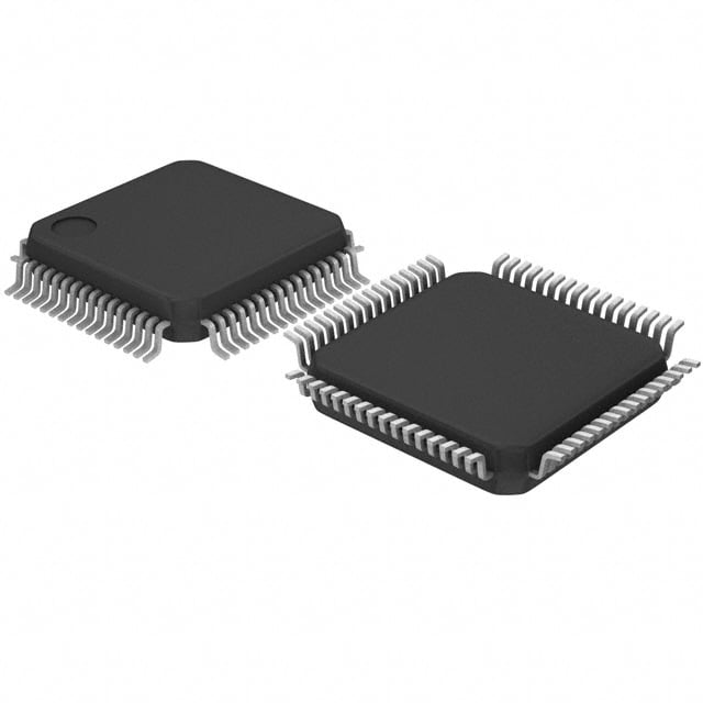
| 供应商器件封装 | 64-LQFP(10x10) |
| 其它名称 | 296-26235-2 |
| 制造商产品页 | http://www.ti.com/general/docs/suppproductinfo.tsp?distId=10&orderablePartNumber=MSP430FE425IPMR |
| 包装 | 带卷 (TR) |
| 外设 | 欠压检测/复位,LCD,POR,PWM,WDT |
| 封装/外壳 | 64-LQFP |
| 工作温度 | -40°C ~ 85°C |
| 振荡器类型 | 内部 |
| 数据转换器 | A/D 3x16b |
| 标准包装 | 1,000 |
| 核心处理器 | MSP430 |
| 核心尺寸 | 16-位 |
| 电压-电源(Vcc/Vdd) | 1.8 V ~ 3.6 V |
| 程序存储器类型 | 闪存 |
| 程序存储容量 | 16KB(16K x 8 + 256B) |
| 连接性 | SPI,UART/USART |
| 速度 | 8.4MHz |


- 商务部:美国ITC正式对集成电路等产品启动337调查
- 曝三星4nm工艺存在良率问题 高通将骁龙8 Gen1或转产台积电
- 太阳诱电将投资9.5亿元在常州建新厂生产MLCC 预计2023年完工
- 英特尔发布欧洲新工厂建设计划 深化IDM 2.0 战略
- 台积电先进制程称霸业界 有大客户加持明年业绩稳了
- 达到5530亿美元!SIA预计今年全球半导体销售额将创下新高
- 英特尔拟将自动驾驶子公司Mobileye上市 估值或超500亿美元
- 三星加码芯片和SET,合并消费电子和移动部门,撤换高东真等 CEO
- 三星电子宣布重大人事变动 还合并消费电子和移动部门
- 海关总署:前11个月进口集成电路产品价值2.52万亿元 增长14.8%


PDF Datasheet 数据手册内容提取
Product Sample & Technical Tools & Support & Folder Buy Documents Software Community MSP430FE427,MSP430FE425,MSP430FE423 SLAS396D–JULY2003–REVISEDNOVEMBER2016 MSP430FE42x Mixed-Signal Microcontrollers 1 Device Overview 1.1 Features 1 • LowSupplyVoltageRange:2.7Vto3.6V • BrownoutDetector • Ultra-LowPowerConsumption: • SupplyVoltageSupervisorandMonitorWith – ActiveMode:400 µAat1MHz,3V ProgrammableLevelDetection – StandbyMode:1.6 µA • SerialOnboardProgramming,NoExternal ProgrammingVoltageNeeded,Programmable – OffMode(RAMRetention):0.1 µA CodeProtectionbySecurityFuse • FivePower-SavingModes • Bootloader(BSL) • WakeupFromStandbyModeinLessThan6µs • FamilyMembersInclude: • Frequency-LockedLoop,FLL+ – MSP430FE423 • 16-BitRISCArchitecture,125-nsInstructionCycle 8KB+256BofFlashMemory,256BofRAM Time – MSP430FE425 • EmbeddedSignalProcessingforSingle-Phase 16KB+256BofFlashMemory,512BofRAM EnergyMeteringWithIntegratedAnalogFrontEnd – MSP430FE427 andTemperatureSensor(ESP430CE1) 32KB+256BofFlashMemory,1KBofRAM • 16-BitTimer_AWithThreeCapture/Compare • Availablein64-PinQuadFlatPack(LQFP) Registers • ForCompleteModuleDescriptions,Seethe • IntegratedLCDDriverfor128Segments MSP430x4xxFamilyUser'sGuide • SerialCommunicationInterface(USART), AsynchronousUARTorSynchronousSPI SelectablebySoftware 1.2 Applications • 2-Wireand3-WireSingle-PhaseMeters • Tamper-ResistantMeters 1.3 Description The TI MSP430™ family of ultra-low-power microcontrollers consists of several devices featuring different sets of peripherals targeted for various applications. The architecture, combined with five low-power modes, is optimized to achieve extended battery life in portable measurement applications. The device features a powerful 16-bit RISC CPU, 16-bit registers, and constant generators that contribute to maximum code efficiency. The digitally controlled oscillator (DCO) allows the device to wake up from low- powermodestoactivemodeinlessthan6µs. The MSP430FE42x series are microcontroller configurations with three independent 16-bit sigma-delta ADCs and an embedded signal processor core used to measure and calculate single-phase energy in both 2-wire and 3-wire configurations. Also included are a built-in 16-bit timer, 128-segment LCD drive capability,and14I/Opins. Typical applications include 2-wire and 3-wire single-phase metering including tamper-resistant meter implementations. 1 An IMPORTANT NOTICE at the end of this data sheet addresses availability, warranty, changes, use in safety-critical applications, intellectualpropertymattersandotherimportantdisclaimers.PRODUCTIONDATA.
MSP430FE427,MSP430FE425,MSP430FE423 SLAS396D–JULY2003–REVISEDNOVEMBER2016 www.ti.com DeviceInformation(1) PARTNUMBER PACKAGE BODYSIZE(2) MSP430FE427IPM LQFP(64) 10mm×10mm MSP430FE425IPM LQFP(64) 10mm×10mm MSP430FE423IPM LQFP(64) 10mm×10mm (1) Forthemostcurrentpart,package,andorderinginformationforallavailabledevices,seethePackage OptionAddenduminSection8,orseetheTIwebsiteatwww.ti.com. (2) Thesizesshownhereareapproximations.Forthepackagedimensionswithtolerances,seethe MechanicalDatainSection8. 1.4 Functional Block Diagram Figure1-1showsthefunctionalblockdiagram. DV DV AV AV XIN XOUT CC SS CC SS P1 P2 8 6 ACLK Oscillators Flash RAM Port 1 Port 2 FLL+ SMCLK Timer_A3 USART0 32KB 1KB 8 I/Os 6 I/Os 16KB 512 B 3 CC Reg Interrupt Interrupt UART MCLK 8KB 256 B Capability Capability or SPI MAB 8-MHz CPU Including 16 Registers MDB Emulation ESP430CE1 Module Basic LCD PSOVSR,, WWatcDhTd+og EmSbigendadled Timer 1 128 Brownout 15 or 16 Bit ProAcneaslosigng, 1 Interrupt 1S,2e,3g,m4 eMnUtsX JTAG Front End Vector Interface f LCD RST/NMI Copyright © 2016,Texas Instruments Incorporated Figure1-1.MSP430FE42xBlockDiagram 2 DeviceOverview Copyright©2003–2016,TexasInstrumentsIncorporated SubmitDocumentationFeedback ProductFolderLinks:MSP430FE427 MSP430FE425 MSP430FE423
MSP430FE427,MSP430FE425,MSP430FE423 www.ti.com SLAS396D–JULY2003–REVISEDNOVEMBER2016 Table of Contents 1 DeviceOverview......................................... 1 5.25 ESP430CE1,SD16ReferenceOutputBuffer....... 24 .............................................. ...... 1.1 Features 1 5.26 ESP430CE1,SD16ExternalReferenceInput 24 1.2 Applications........................................... 1 5.27 ESP430CE1,ActiveEnergyMeasurementTest ............................ ............................................ ConditionsandAccuracy 25 1.3 Description 1 ............................ 5.28 ESP430CE1,ActiveEnergyMeasurementTest 1.4 FunctionalBlockDiagram 2 ............................ ConditionsandAccuracy 25 2 Revision History......................................... 4 5.29 ESP430CE1TypicalCharacteristics(I1SD16GAINx 3 DeviceComparison ..................................... 5 =1).................................................. 27 ..................................... 3.1 RelatedProducts 5 5.30 ESP430CE1TypicalCharacteristics(I1SD16GAINx 4 TerminalConfigurationandFunctions.............. 6 =4).................................................. 28 4.1 PinDiagram.......................................... 6 5.31 ESP430CE1TypicalCharacteristics(I1SD16GAINx .................................................. ................................... =8) 29 4.2 SignalDescriptions 7 5 Specifications........................................... 10 5.32 ESP4.3.0.C..E..1..T.y.p..ic..a.l.C..h.a..ra..c.t.e.r.is.t.i.c.s..(.I1..S..D..1.6.G..A..IN..x =32) 30 ........................ 5.1 AbsoluteMaximumRatings 10 ....................................... 5.33 FlashMemory 31 ........................................ 5.2 ESDRatings 10 ...................................... 5.34 JTAGInterface 31 ............... 5.3 RecommendedOperatingConditions 10 ......................................... 5.35 JTAGFuse 31 5.4 SupplyCurrentInt.o..A..V.C..C..a.n.d..D..V..C.C..E..x.c.l.u.d.i.n.g...... 6 DetailedDescription................................... 32 ExternalCurrent 11 ................................................. 6.1 CPU 32 5.5 ThermalResistanceCharacteristics,PMPackage (LQFP64)............................................ 12 6.2 InstructionSet....................................... 33 .................................... 5.6 Schmitt-TriggerInputs−Ports(P1andP2), 6.3 OperatingModes 34 RST/NMI,JTAG(TCK,TMS,TDI/TCLK,TDO/TDI). 12 6.4 InterruptVectorAddresses.......................... 35 5.7 InputsP1.x,P2.x,TAx.............................. 12 6.5 SpecialFunctionRegisters.......................... 36 5.8 LeakageCurrent−Ports(P1andP2) ............. 12 6.6 Memory Organization............................... 38 5.9 Outputs−Ports(P1andP2)........................ 13 6.7 Bootloader(BSL).................................... 38 5.10 OutputFrequency................................... 13 6.8 FlashMemory....................................... 38 5.11 TypicalCharacteristics–PortsP1andP2.......... 14 6.9 Peripherals.......................................... 39 5.12 Wake-upTimeFromLPM3......................... 15 6.10 Input/OutputDiagrams.............................. 45 5.13 RAM................................................. 15 7 DeviceandDocumentationSupport............... 52 5.14 LCD.................................................. 15 7.1 GettingStartedandNextSteps..................... 52 5.15 USART0............................................. 15 7.2 Device Nomenclature............................... 52 5.16 POR,BOR .......................................... 16 7.3 ToolsandSoftware................................. 54 5.17 SVS(SupplyVoltageSupervisorandMonitor)..... 17 7.4 DocumentationSupport............................. 55 5.18 DCO................................................. 19 7.5 RelatedLinks........................................ 57 5.19 CrystalOscillator,LFXT1Oscillator ................ 21 7.6 CommunityResources.............................. 57 5.20 ESP430CE1,SD16andESP430PowerSupplyand .......................................... 7.7 Trademarks 57 ................................ OperatingConditions 22 ..................... 7.8 ElectrostaticDischargeCaution 57 ................... 5.21 ESP430CE1,SD16InputRange 22 ............................... 7.9 ExportControlNotice 57 ................... 5.22 ESP430CE1,SD16Performance 23 ............................................. 7.10 Glossary 57 ........... 5.23 ESP430CE1,SD16TemperatureSensor 23 8 Mechanical,Packaging,andOrderable ..... 5.24 ESP430CE1,SD16Built-inVoltageReference 24 Information.............................................. 58 Copyright©2003–2016,TexasInstrumentsIncorporated TableofContents 3 SubmitDocumentationFeedback ProductFolderLinks:MSP430FE427 MSP430FE425 MSP430FE423
MSP430FE427,MSP430FE425,MSP430FE423 SLAS396D–JULY2003–REVISEDNOVEMBER2016 www.ti.com 2 Revision History NOTE:Pagenumbersforpreviousrevisionsmaydifferfrompagenumbersinthecurrentversion. ChangesfromOctober16,2008toNovember14,2016 Page • Formatandorganizationchangesthroughoutdocument,includingadditionofsectionnumbering....................... 1 • AddedSection3...................................................................................................................... 5 • AddedSection5andmovedallelectricalandtimingspecificationstoit.................................................... 10 • AddedSection5.2,ESDRatings.................................................................................................. 10 • ChangedtheMAXvalueoftheI parameterat85°Cfrom2.6to3.5µAinSection5.4,SupplyCurrentInto (LPM3) AV andDV ExcludingExternalCurrent..................................................................................... 11 CC CC • AddedSection5.5,ThermalResistanceCharacteristics,PMPackage(LQFP-64)........................................ 12 • Changedallcasesof"bootstraploader"to"bootloader"....................................................................... 38 • ChangedthevalueofthePort/LCDcolumninTable6-14,PortP1(P1.2toP1.7)PinFunctions....................... 46 • ChangedthevalueofthePort/LCDcolumninTable6-15,PortP2(P2.0andP2.1)PinFunctions..................... 47 • AddedSection7,DeviceandDocumentationSupport......................................................................... 52 • AddedSection8,Mechanical,Packaging,andOrderableInformation...................................................... 58 4 RevisionHistory Copyright©2003–2016,TexasInstrumentsIncorporated SubmitDocumentationFeedback ProductFolderLinks:MSP430FE427 MSP430FE425 MSP430FE423
MSP430FE427,MSP430FE425,MSP430FE423 www.ti.com SLAS396D–JULY2003–REVISEDNOVEMBER2016 3 Device Comparison Table3-1summarizestheavailablefamilymembers. Table3-1.DeviceComparison(1)(2) FLASH RAM FREQUENCY DEVICE BSL ESP430 I/O PACKAGE (KB) (B) (MHz) MSP430F427 32 1K 8 UART 1 14 PM64 MSP430F425 16 512 8 UART 1 14 PM64 MSP430F423 8 256 8 UART 1 14 PM64 (1) Forthemostcurrentpackageandorderinginformation,seethePackageOptionAddenduminSection8,orseetheTIwebsiteat www.ti.com. (2) Packagedrawings,thermaldata,andsymbolizationareavailableatwww.ti.com/packaging. 3.1 Related Products Forinformationaboutotherdevicesinthisfamilyofproductsorrelatedproducts,seethefollowinglinks. TIMicrocontrollersProductSelection TI's low-power and-high performance MCUs, with wired and wirelessconnectivityoptions,areoptimizedforabroadrangeofapplications. ProductsforMSP430Ultra-Low-PowerMicrocontrollers One platform. One ecosystem. Endless possibilities. Enabling the connected world with innovations in ultra-low-power microcontrollerswithadvancedperipheralsforprecisesensingandmeasurement. ProductsforMSP430F2x/4xUltra-Low-PowerMicrocontrollers MSP430F2x/4x microcontrollers (MCUs) from the MSP ultra-low-power MCU series are general-purpose 16-bit microcontrollers used for a wide range of applications including consumer electronics, data logging applications, portable medical instruments, and low-power metering. MSP430F4x MCUs feature an integrated LCD controller, while select MSP430F2x devices feature extendedtemperatureranges. CompanionProductsforMSP430FE427 Review products that are frequently purchased or used with thisproduct. ReferenceDesigns The TI Designs Reference Design Library is a robust reference design library that spans analog, embedded processor, and connectivity. Created by TI experts to help you jump start your system design, all TI Designs include schematic or block diagrams, BOMs, anddesignfilestospeedyourtimetomarket. Copyright©2003–2016,TexasInstrumentsIncorporated DeviceComparison 5 SubmitDocumentationFeedback ProductFolderLinks:MSP430FE427 MSP430FE425 MSP430FE423
MSP430FE427,MSP430FE425,MSP430FE423 SLAS396D–JULY2003–REVISEDNOVEMBER2016 www.ti.com 4 Terminal Configuration and Functions 4.1 Pin Diagram Figure4-1showsthepinoutforthe64-pinPMpackage. 0 3 K S N D0 D0 MCL S31 OUT/ SVSI UTX URX NMI CLK TDI TA0 TA0/ TA1/ SVS S29 AVCC DVSS AVSSP2.3/ P2.4/ P2.5/ RST/ TCK TMS TDI/T TDO/ P1.0/ P1.1/ P1.2/ P1.3/ P1.4/ 6463 6261 60 59 58 57 56 55 54 53 52 51 5049 DV 1 48 P1.5/TACLK/ACLK/S28 CC I1+ 2 47 P1.6/SIMO0/S27 I1− 3 46 P1.7/SOMI0/S26 I2+ 4 45 P2.0/TA2/S25 I2− 5 44 P2.1/UCLK0/S24 V1+ 6 43 R33 V1− 7 42 R23 XIN 8 41 R13 XOUT 9 40 R03 VREF 10 39 COM3 P2.2/STE0 11 38 COM2 S0 12 37 COM1 S1 13 36 COM0 S2 14 35 S23 S3 15 34 S22 S4 16 33 S21 17 18 19 20 21 22 23 24 25 26 27 28 29 30 31 32 5 6 7 8 9 0 1 2 3 4 5 6 7 8 9 0 S S S S S 1 1 1 1 1 1 1 1 1 1 2 S S S S S S S S S S S NOTE: TIrecommendsleavingallunusedanaloginputsopen. Figure4-1.64-PinPMPackage(TopView) 6 TerminalConfigurationandFunctions Copyright©2003–2016,TexasInstrumentsIncorporated SubmitDocumentationFeedback ProductFolderLinks:MSP430FE427 MSP430FE425 MSP430FE423
MSP430FE427,MSP430FE425,MSP430FE423 www.ti.com SLAS396D–JULY2003–REVISEDNOVEMBER2016 4.2 Signal Descriptions Table4-1describesthesignalsforalldevicevariants Table4-1.TerminalFunctions SIGNALNAME PINNO. I/O DESCRIPTION DVCC 1 Digitalsupplyvoltage,positiveterminal I1+ 2 I Current1positiveanaloginput,internalconnectiontoSD16channel0A0+(1) I1− 3 I Current1negativeanaloginput,internalconnectiontoSD16channel0A0−(1) I2+ 4 I Current2positiveanaloginput,internalconnectiontoSD16channel1A0+(1) I2− 5 I Current2negativeanaloginput,internalconnectiontoSD16channel1A0−(1) V1+ 6 I Voltage1positiveanaloginput,internalconnectiontoSD16channel2A0+(1) V1− 7 I Voltage1negativeanaloginput,internalconnectiontoSD16channel2A0−(1) XIN 8 I InputportforcrystaloscillatorXT1.Standardorwatchcrystalscanbeconnected. XOUT 9 O OutputterminalofcrystaloscillatorXT1 Inputforanexternalreferencevoltage,internalreferencevoltageoutput(canbeusedas V 10 I/O REF mid-voltage) General-purposedigitalI/O P2.2/STE0 11 I/O SlavetransmitenableforUSART0inSPImode S0 12 O LCDsegmentoutput0 S1 13 O LCDsegmentoutput1 S2 14 O LCDsegmentoutput2 S3 15 O LCDsegmentoutput3 S4 16 O LCDsegmentoutput4 S5 17 O LCDsegmentoutput5 S6 18 O LCDsegmentoutput6 S7 19 O LCDsegmentoutput7 S8 20 O LCDsegmentoutput8 S9 21 O LCDsegmentoutput9 S10 22 O LCDsegmentoutput10 S11 23 O LCDsegmentoutput11 S12 24 O LCDsegmentoutput12 S13 25 O LCDsegmentoutput13 S14 26 O LCDsegmentoutput14 S15 27 O LCDsegmentoutput15 S16 28 O LCDsegmentoutput16 S17 29 O LCDsegmentoutput17 S18 30 O LCDsegmentoutput18 S19 31 O LCDsegmentoutput19 S20 32 O LCDsegmentoutput20 S21 33 O LCDsegmentoutput21 S22 34 O LCDsegmentoutput22 S23 35 O LCDsegmentoutput23 COM0 36 O Commonoutput,COM0−COM3areusedforLCDbackplanes. COM1 37 O Commonoutput,COM0−COM3areusedforLCDbackplanes. COM2 38 O Commonoutput,COM0−COM3areusedforLCDbackplanes. COM3 39 O Commonoutput,COM0−COM3areusedforLCDbackplanes. R03 40 I Inputportoffourthpositive(lowest)analogLCDlevel(V5) R13 41 I InputportofthirdmostpositiveanalogLCDlevel(V4orV3) R23 42 I InputportofsecondmostpositiveanalogLCDlevel(V2) (1) TIrecommendsopenconnectionforallunusedanaloginputs. Copyright©2003–2016,TexasInstrumentsIncorporated TerminalConfigurationandFunctions 7 SubmitDocumentationFeedback ProductFolderLinks:MSP430FE427 MSP430FE425 MSP430FE423
MSP430FE427,MSP430FE425,MSP430FE423 SLAS396D–JULY2003–REVISEDNOVEMBER2016 www.ti.com Table4-1.TerminalFunctions(continued) SIGNALNAME PINNO. I/O DESCRIPTION R33 43 O OutputportofmostpositiveanalogLCDlevel(V1) General-purposedigitalI/O ExternalclockinputforUSART0inUARTorSPImode,or P2.1/UCLK0/S24 44 I/O clockoutputforUSART0inSPImode LCDsegmentoutput24(2) General-purposedigitalI/O P2.0/TA2/S25 45 I/O Timer_ACapture:CCI2Ainput,Compare:Out2output LCDsegmentoutput25(2) General-purposedigitalI/O P1.7/SOMI0/S26 46 I/O Slaveout/masterinforUSART0inSPImode LCDsegmentoutput26(2) General-purposedigitalI/O P1.6/SIMO0/S27 47 I/O Slavein/masteroutforUSART0inSPImode LCDsegmentoutput27(2) General-purposedigitalI/O Timer_AandSD16clocksignalTACLKinput P1.5/TACLK/ACLK/S28 48 I/O ACLKoutput(dividedby1,2,4,or8) LCDsegmentoutput28(2) General-purposedigitalI/O P1.4/S29 49 I/O LCDsegmentoutput29(2) General-purposedigitalI/O P1.3/SVSOUT/S30 50 I/O SVS:outputofSVScomparator LCDsegmentoutput30(2) General-purposedigitalI/O P1.2/TA1/S31 51 I/O Timer_A,Capture:CCI1A,CCI1Binput,Compare:Out1output LCDsegmentoutput31(2) General-purposedigitalI/O Timer_A,Capture:CCI0Binput.Note:TA0isonlyaninputonthispin. P1.1/TA0/MCLK 52 I/O MCLKoutput BSLreceive General-purposedigitalI/O P1.0/TA0 53 I/O Timer_A,Capture:CCI0Ainput,Compare:Out0output BSLtransmit TDO/TDI 54 I/O Testdataoutputport,TDO/TDIdataoutputorprogrammingdatainputterminal TDI/TCLK 55 I Testdatainputortestclockinput.ThedeviceprotectionfuseisconnectedtoTDI. TMS 56 I Testmodeselect.TMSisusedasaninputportfordeviceprogrammingandtest. TCK 57 I Testclock.TCKistheclockinputportfordeviceprogrammingandtest. RST/NMI 58 I Resetinputornonmaskableinterruptinputport General-purposedigitalI/O P2.5/URXD0 59 I/O ReceivedatainforUSART0inUARTmode General-purposedigitalI/O P2.4/UTXD0 60 I/O TransmitdataoutforUSART0inUARTmode (2) LCDfunctionselectedautomaticallywhenapplicableLCDmodulecontrolbitsareset,notwithPxSELbits. 8 TerminalConfigurationandFunctions Copyright©2003–2016,TexasInstrumentsIncorporated SubmitDocumentationFeedback ProductFolderLinks:MSP430FE427 MSP430FE425 MSP430FE423
MSP430FE427,MSP430FE425,MSP430FE423 www.ti.com SLAS396D–JULY2003–REVISEDNOVEMBER2016 Table4-1.TerminalFunctions(continued) SIGNALNAME PINNO. I/O DESCRIPTION General-purposedigitalI/O P2.3/SVSIN 61 I/O Analoginputtobrownout,supplyvoltagesupervisor Analogsupplyvoltage,negativeterminal.SuppliesSD16,SVS,brownout,oscillator,and AV 62 SS LCDresistivedividercircuitry. DV 63 Digitalsupplyvoltage,negativeterminal SS Analogsupplyvoltage,positiveterminal.SuppliesSD16,SVS,brownout,oscillator,and AV 64 CC LCDresistivedividercircuitry.DonotpowerupbeforeDVCC. Copyright©2003–2016,TexasInstrumentsIncorporated TerminalConfigurationandFunctions 9 SubmitDocumentationFeedback ProductFolderLinks:MSP430FE427 MSP430FE425 MSP430FE423
MSP430FE427,MSP430FE425,MSP430FE423 SLAS396D–JULY2003–REVISEDNOVEMBER2016 www.ti.com 5 Specifications 5.1 Absolute Maximum Ratings(1) overoperatingfree-airtemperaturerange(unlessotherwisenoted) MIN MAX UNIT VoltageappliedatV toV –0.3 4.1 V CC SS Voltageappliedtoanypin(2) –0.3 V +0.3 V CC Diodecurrentatanydeviceterminal ±2 mA Unprogrammeddevice –55 150 Storagetemperaturerange,T °C stg Programmeddevice –40 85 (1) StressesbeyondthoselistedunderAbsoluteMaximumRatingsmaycausepermanentdamagetothedevice.Thesearestressratings only,andfunctionaloperationofthedeviceattheseoranyotherconditionsbeyondthoseindicatedunderRecommendedOperating Conditionsisnotimplied.Exposuretoabsolute-maximum-ratedconditionsforextendedperiodsmayaffectdevicereliability. (2) AllvoltagesreferencedtoV .TheJTAGfuse-blowvoltage,V ,isallowedtoexceedtheabsolutemaximumrating.Thevoltageis SS FB appliedtotheTDI/TCLKpinwhenblowingtheJTAGfuse. 5.2 ESD Ratings VALUE UNIT Human-bodymodel(HBM),perANSI/ESDA/JEDECJS-001(1) ±1000 V Electrostaticdischarge V (ESD) Charged-devicemodel(CDM),perJEDECspecificationJESD22-C101(2) ±250 (1) JEDECdocumentJEP155statesthat500-VHBMallowssafemanufacturingwithastandardESDcontrolprocess.Pinslistedas ±1000Vmayactuallyhavehigherperformance. (2) JEDECdocumentJEP157statesthat250-VCDMallowssafemanufacturingwithastandardESDcontrolprocess.Pinslistedas±250V mayactuallyhavehigherperformance. 5.3 Recommended Operating Conditions TypicalvaluesarespecifiedatV =3.3VandT =25°C(unlessotherwisenoted) CC A MIN NOM MAX UNIT ESP430andSD16disabled 1.8 3.6 SVSenabled,PORON=1(2),ESP430andSD16 Supplyvoltageduringprogram 2.0 3.6 VCC execution(1)(AV =DV =V ) disabled V CC CC CC ESP430orSD16enabledorduringprogrammingof 2.7 3.6 flashmemory V Supplyvoltage(AV =DV =V ) 0 0 V SS SS SS SS T Operatingfree-airtemperaturerange –40 85 °C A LFselected,XTS_FLL=0 Watchcrystal 32.768 f LFXT1crystalfrequency(3) XT1selected,XTS_FLL=1 Ceramicresonator 450 8000 kHz (LFXT1) XT1selected,XTS_FLL=1 Crystal 1000 8000 Processorfrequency(signal VCC=2.7V DC 8.4 f(System) MCLK)(4)(alsoseeFigure5-1) V =3.6V DC 8.4 MHz CC (1) TIrecommendspoweringAV andDV fromthesamesource.Amaximumdifferenceof0.3VbetweenAV andDV canbe CC CC CC CC toleratedduringpowerupandoperation. (2) TheminimumoperatingsupplyvoltageisdefinedaccordingtothetrippointwherePORisgoingactivebydecreasingthesupply voltage.PORisgoinginactivewhenthesupplyvoltageisraisedabovetheminimumsupplyvoltageplusthehysteresisoftheSVS circuitry. (3) InLFmode,theLFXT1oscillatorrequiresawatchcrystal. (4) Forfrequenciesabove8MHz,MCLKissourcedbythebuilt-inoscillator(DCOandFLL+). 10 Specifications Copyright©2003–2016,TexasInstrumentsIncorporated SubmitDocumentationFeedback ProductFolderLinks:MSP430FE427 MSP430FE425 MSP430FE423
MSP430FE427,MSP430FE425,MSP430FE423 www.ti.com SLAS396D–JULY2003–REVISEDNOVEMBER2016 Frequency Supply voltage range with ESP430 or SD16 enabled and during z programming of the flash memory H M 8.4 MHz − y c n e Supply voltage range u q during program execution e or Fr 6 MHz s s e c o Pr 4.15 MHz m u m xi a M − fSystem 1.8 V 2.7V 3V 3.6 V V −Supply Voltage−V CC Figure5-1.FrequencyvsSupplyVoltage 5.4 Supply Current Into AV and DV Excluding External Current(1) CC CC overrecommendedoperatingfree-airtemperaturerange(unlessotherwisenoted) PARAMETER T V MIN TYP MAX UNIT A CC Activemode(AM) f =f =f =1MHz, I (MCLK) (SMCLK) (DCO) –40°Cto85°C 3V 400 500 µA (AM) f =32768Hz,XTS_FLL=0, (ACLK) programexecutesinflash Low-powermode0or1(LPM0orLPM1)(2) f =f =f =1MHz, I (MCLK) (SMCLK) (DCO) –40°Cto85°C 3V 130 150 µA (LPM0) f =32768Hz,XTS_FLL=0, (ACLK) FN_8=FN_4=FN_3=FN_2=0 I Low-powermode2(LPM2)(2) –40°Cto85°C 3V 10 22 µA (LPM2) –40°C 1.5 2.0 25°C 1.6 2.1 I Low-powermode3(LPM3) (2) 3V µA (LPM3) 60°C 1.7 2.2 85°C 2.0 3.5 –40°C 0.1 0.5 I Low-powermode4(LPM4)(2) 25°C 3V 0.1 0.5 µA (LPM4) 85°C 0.8 2.5 (1) Allinputsaretiedto0VorV .Outputsdonotsourceorsinkanycurrent.ThecurrentconsumptioninLPM2,LPM3,andLPM4are CC measuredwithactiveBasicTimer1andLCD(ACLKselected).ThecurrentconsumptionoftheESP430CE1andtheSVSmoduleare specifiedintheirrespectivesections.LPMxcurrentsmeasuredwithWDT+disabled.ThecurrentsarecharacterizedwithaKDS DaishinkuDT−38(6pF)crystal. (2) Currentconsumptionforbrownoutisincluded. Currentconsumptionofactivemodeversussystemfrequency: I =I [1MHz]× f [MHz] (AM) (AM) (System) Currentconsumptionofactivemodeversussupplyvoltage: I =I [3V]+170 µA/V × (V –3V) (AM) (AM) CC Copyright©2003–2016,TexasInstrumentsIncorporated Specifications 11 SubmitDocumentationFeedback ProductFolderLinks:MSP430FE427 MSP430FE425 MSP430FE423
MSP430FE427,MSP430FE425,MSP430FE423 SLAS396D–JULY2003–REVISEDNOVEMBER2016 www.ti.com 5.5 Thermal Resistance Characteristics, PM Package (LQFP64) PARAMETER VALUE UNIT Rθ Junction-to-ambientthermalresistance,stillair(1) 55.7 °C/W JA Rθ Junction-to-case(top)thermalresistance(2) 16.7 °C/W JC(TOP) Rθ Junction-to-boardthermalresistance(3) 27.1 °C/W JB Ψ Junction-to-boardthermalcharacterizationparameter 26.8 °C/W JB Ψ Junction-to-topthermalcharacterizationparameter 0.8 °C/W JT (1) Thejunction-to-ambientthermalresistanceundernaturalconvectionisobtainedinasimulationonaJEDEC-standard,High-Kboard,as specifiedinJESD51-7,inanenvironmentdescribedinJESD51-2a. (2) Thejunction-to-case(top)thermalresistanceisobtainedbysimulatingacoldplatetestonthepackagetop.NospecificJEDEC- standardtestexists,butaclosedescriptioncanbefoundintheANSISEMIstandardG30-88. (3) Thejunction-to-boardthermalresistanceisobtainedbysimulatinginanenvironmentwitharingcoldplatefixturetocontrolthePCB temperature,asdescribedinJESD51-8. 5.6 Schmitt-Trigger Inputs − Ports (P1 and P2), RST/NMI, JTAG (TCK, TMS, TDI/TCLK,TDO/TDI) overrecommendedoperatingfree-airtemperaturerange(unlessotherwisenoted) PARAMETER V MIN MAX UNIT CC V Positive-goinginputthresholdvoltage 3V 1.5 1.98 V IT+ V Negative-goinginputthresholdvoltage 3V 0.9 1.3 V IT- V Inputvoltagehysteresis(V -V ) 3V 0.45 1 V hys IT+ IT- 5.7 Inputs P1.x, P2.x, TAx overrecommendedoperatingfree-airtemperaturerange(unlessotherwisenoted) PARAMETER TESTCONDITIONS V MIN MAX UNIT CC PortP1,P2:P1.xtoP2.x,externaltriggersignal 1.5 cycle t(int) Externalinterrupttiming fortheinterruptflag(1) 3V 50 ns t Timer_Acapturetiming TAx 3V 50 ns (cap) Timer_Aclockfrequencyexternally f TAxCLK,INCLKt =t 3V 10 MHz (TAext) appliedtopin (H) (L) f Timer_Aclockfrequency SMCLKorACLKsignalselected 3V 10 MHz (TAint) (1) Theexternalsignalsetstheinterruptflageverytimetheminimumt parametersaremet.Itmaybesetevenwithtriggersignals (int) shorterthant .Boththecycleandtimingspecificationsmustbemettoensuretheflagisset.t ismeasuredinMCLKcycles. (int) (int) 5.8 Leakage Current − Ports (P1 and P2)(1) overrecommendedoperatingfree-airtemperaturerange(unlessotherwisenoted) PARAMETER TESTCONDITIONS V MIN MAX UNIT CC I Leakagecurrent,PortP1.x Port1:V (2) 3V ±50 nA lkg(P1.x) (P1.x) I Leakagecurrent,PortP2.x Port2:V (2) 3V ±50 nA lkg(P2.x) (P2.x) (1) TheleakagecurrentismeasuredwithV orV appliedtothecorrespondingpins,unlessotherwisenoted. SS CC (2) Theportpinmustbeselectedasinput. 12 Specifications Copyright©2003–2016,TexasInstrumentsIncorporated SubmitDocumentationFeedback ProductFolderLinks:MSP430FE427 MSP430FE425 MSP430FE423
MSP430FE427,MSP430FE425,MSP430FE423 www.ti.com SLAS396D–JULY2003–REVISEDNOVEMBER2016 5.9 Outputs − Ports (P1 and P2) overrecommendedoperatingfree-airtemperaturerange(unlessotherwisenoted) PARAMETER TESTCONDITIONS V MIN MAX UNIT CC I =–1.5mA(1) 3V V –0.25 V OH(max) CC CC V High-leveloutputvoltage V OH I =–6mA(2) 3V V –0.6 V OH(max) CC CC I =1.5mA(1) 3V V V +0.25 OL(max) SS SS V Low-leveloutputvoltage V OL I =6mA(2) 3V V V +0.6 OL(max) SS SS (1) Themaximumtotalcurrent,I andI ,foralloutputscombined,shouldnotexceed±12mAtosatisfythemaximumspecified OH(max) OL(max) voltagedrop. (2) Themaximumtotalcurrent,I andI ,foralloutputscombined,shouldnotexceed±48mAtosatisfythemaximumspecified OH(max) OL(max) voltagedrop. 5.10 Output Frequency overrecommendedoperatingfree-airtemperaturerange(unlessotherwisenoted) PARAMETER TESTCONDITIONS MIN TYP MAX UNIT Outputfrequency f C =20F,I =±1.5mA,V =3V DC 12 MHz (Px.y) (1≤×≤2,0≤y≤7) L L CC f , (ACLK) P1.1/TA0/MCLK, f , C =20pF,V =3V 12 MHz (MCLK) P1.5/TACLK/ACLK/S28 L CC f (SMCLK) f =f =f 40% 60% ACLK LFXT1 XT1 P1.5/TACLK/ACLK/S28, f =f =f 30% 70% Dutycycleofoutput CL=20pF,VCC=3V ACLK LFXT1 LF t(Xdc) frequency fACLK=fLFXT1 50% P1.1/TA0/MCLK,C =20pF,V =3V, 50%– 50%+ L CC 50% f =f 15ns 15ns MCLK DCOCLK Copyright©2003–2016,TexasInstrumentsIncorporated Specifications 13 SubmitDocumentationFeedback ProductFolderLinks:MSP430FE427 MSP430FE425 MSP430FE423
MSP430FE427,MSP430FE425,MSP430FE423 SLAS396D–JULY2003–REVISEDNOVEMBER2016 www.ti.com 5.11 Typical Characteristics – Ports P1 and P2 Figure5-2throughFigure5-5 showthetypicaloutputcurrentsofPortsP1andP2.Oneoutputloadedata time. 30 50 V = 2.2 V V = 3 V P2CC.1 TA= 25°C P2CC.1 TA= 25°C mA 25 mA 40 − − Current 20 TA= 85°C Current TA= 85°C ut ut 30 p p ut ut O O el 15 el v v e e L L w- w- 20 o o al L 10 al L c c pi pi Ty Ty − − 10 IOL 5 IOL 0 0 0.0 0.5 1.0 1.5 2.0 2.5 0.0 0.5 1.0 1.5 2.0 2.5 3.0 3.5 V −Low-Level Output Voltage−V V −Low-Level Output Voltage−V OL OL Figure5-2.TypicalLow-LevelOutputCurrentvs Figure5-3.TypicalLow-LevelOutputCurrentvs Low-LevelOutputVoltage Low-LevelOutputVoltage 0 0 VP2CC.1= 2.2 V A VP2CC.1= 3 V mA −5 −m −10 − nt put Current −10 utput Curre −20 ut O gh-Level O −15 High-Level −30 cal Hi −20 TA= 85°C pical ypi Ty T = 85°C T − −40 A I−OH −25 TA= 25°C IOH T = 25°C A −30 −50 0.0 0.5 1.0 1.5 2.0 2.5 0.0 0.5 1.0 1.5 2.0 2.5 3.0 3.5 V −High-Level Output Voltage−V V −High-Level Output Voltage−V OH OH Figure5-4.TypicalHigh-LevelOutputCurrentvs Figure5-5.TypicalHigh-LevelOutputCurrentvs High-LevelOutputVoltage High-LevelOutputVoltage 14 Specifications Copyright©2003–2016,TexasInstrumentsIncorporated SubmitDocumentationFeedback ProductFolderLinks:MSP430FE427 MSP430FE425 MSP430FE423
MSP430FE427,MSP430FE425,MSP430FE423 www.ti.com SLAS396D–JULY2003–REVISEDNOVEMBER2016 5.12 Wake-up Time From LPM3 overrecommendedoperatingfree-airtemperaturerange(unlessotherwisenoted) PARAMETER TESTCONDITIONS MIN MAX UNIT f=1MHz 6 t Delaytime f=2MHz V =3V 6 µs d(LPM3) CC f=3MHz 6 5.13 RAM overrecommendedoperatingfree-airtemperaturerange(unlessotherwisenoted) PARAMETER TESTCONDITIONS MIN MAX UNIT V CPUhalted(1) 1.6 V RAMh (1) ThisparameterdefinestheminimumsupplyvoltagewhenthedatainprogrammemoryRAMremainunchanged.Noprogramexecution shouldtakeplaceduringthissupplyvoltagecondition. 5.14 LCD overrecommendedoperatingfree-airtemperaturerange(unlessotherwisenoted) PARAMETER TESTCONDITIONS MIN TYP MAX UNIT V VoltageatR33 2.5 V +0.2 V (33) CC [V –V ]× V VoltageatR23 (33) (03) (23) 2/3+V (03) Analogvoltage V =3V CC [V –V ]× V VoltageatR13 (33) (03) (13) 1/3+V (03) V –V VoltageatR33toR03 2.5 V +0.2 (33) (03) CC I R03=V Noloadatall ±20 (R03) SS segmentand I(R13) Inputleakage R13=VCC/3 commonlines, ±20 nA I(R23) R23=2×VCC/3 VCC=3V ±20 V V ) V –0.1 (Sxx0) (03 (03) V V V –0.1 (Sxx1) (13) (13) Segmentlinevoltage I =–3µA,V =3V V (Sxx) CC V V V –0.1 (Sxx2) (23) (23) V V ) V +0.1 (Sxx3) (33 (33) 5.15 USART0(1) overrecommendedoperatingfree-airtemperaturerange(unlessotherwisenoted) PARAMETER TESTCONDITIONS MIN TYP MAX UNIT t USART0deglitchtime V =3V,SYNC=0,UARTmode 150 280 500 ns (τ) CC (1) ThesignalappliedtotheUSART0receivesignal/terminal(URXD0)shouldmeetthetimingrequirementsoft(τ)toensurethattheURXS flip-flopisset.TheURXSflip-flopissetwithnegativepulsesmeetingtheminimum-timingconditionoft(τ).Theoperatingconditionsto settheflagmustbemetindependentlyfromthistimingconstraint.Thedeglitchcircuitryisactiveonlyonnegativetransitionsonthe URXD0line. Copyright©2003–2016,TexasInstrumentsIncorporated Specifications 15 SubmitDocumentationFeedback ProductFolderLinks:MSP430FE427 MSP430FE425 MSP430FE423
MSP430FE427,MSP430FE425,MSP430FE423 SLAS396D–JULY2003–REVISEDNOVEMBER2016 www.ti.com 5.16 POR, BOR(1) overrecommendedoperatingfree-airtemperaturerange(unlessotherwisenoted) PARAMETER TESTCONDITIONS MIN TYP MAX UNIT t 2000 µs d(BOR) 0.7× V dV /dt≤3V/s(seeFigure5-6) V CC(start) CC V (B_IT–) V Brownout(2) dV /dt≤3V/s(seeFigure5-6throughFigure5-8) 1.71 V (B_IT–) CC V dV /dt≤3V/s(seeFigure5-6) 70 130 180 mV hys(B_IT–) CC PulsedurationneededatRST/NMIpintoaccept t 2 µs (reset) resetinternally,V =3V CC (1) ThecurrentconsumptionofthebrownoutmoduleisalreadyincludedintheI currentconsumptiondata.ThevoltagelevelV + CC (B_IT–) V ≤1.8V. hys(B_IT–) (2) Duringpowerup,theCPUbeginscodeexecutionfollowingaperiodoft afterV =V +V .ThedefaultFLL+settings d(BOR) CC (B_IT–) hys(B_IT–) mustnotbechangeduntilV ≥V ,whereV istheminimumsupplyvoltageforthedesiredoperatingfrequency.Seethe CC CC(min) CC(min) MSP430x4xxFamilyUser'sGuideformoreinformationonthebrownoutandSVScircuit. V CC V hys(B_IT−) V (B_IT−) V CC(start) 1 0 t d(BOR) Figure5-6.PORandBORvsSupplyVoltage 2 VCC tpw VTyCCpi=c a3l VConditions 3V 1.5 V − VCC(drop) 1 V CC(drop) 0.5 0 0.001 1 1000 1 ns 1 ns t −Pulse Width−µs t −Pulse Width−µs pw pw Figure5-7.V LevelWithaRectangularVoltageDroptoGenerateaPOR/BrownoutSignal CC(drop) 16 Specifications Copyright©2003–2016,TexasInstrumentsIncorporated SubmitDocumentationFeedback ProductFolderLinks:MSP430FE427 MSP430FE425 MSP430FE423
MSP430FE427,MSP430FE425,MSP430FE423 www.ti.com SLAS396D–JULY2003–REVISEDNOVEMBER2016 2 VCC tpw V = 3 V 3V TyCCpical Conditions 1.5 V − VCC(drop) 1 V CC(drop) 0.5 t= t f r 0 0.001 1 1000 t t f r t −Pulse Width−µs t −Pulse Width−µs pw pw Figure5-8.V LevelWithaTriangularVoltageDroptoGenerateaPORorBORSignal CC(drop) 5.17 SVS (Supply Voltage Supervisor and Monitor)(1) overrecommendedoperatingfree-airtemperaturerange(unlessotherwisenoted)(alsoseeFigure5-10) PARAMETER TESTCONDITIONS MIN TYP MAX UNIT dV /dt>30V/ms(seeFigure5-9) 5 150 CC t µs (SVSR) dV /dt≤30V/ms 2000 CC t SVSon,switchfromVLD=0toVLD≠0,V =3V 20 150 µs d(SVSon) CC t VLD≠0(2) 12 µs settle V VLD≠0,V /dt≤3V/s(seeFigure5-9) 1.55 1.7 V (SVSstart) CC VLD=1 70 120 155 mV VCC/dt≤3V/s(seeFigure5-9) VLD=2to14 V(SVS_IT–) V(SVS_IT–) V ×0.004 ×0.008 hys(SVS_IT–) V /dt≤3V/s(seeFigure5-9),externalvoltage CC VLD=15 4.4 10.4 mV appliedonP2.3 VLD=1 1.8 1.9 2.05 VLD=2 1.94 2.1 2.25 VLD=3 2.05 2.2 2.37 VLD=4 2.14 2.3 2.48 VLD=5 2.24 2.4 2.6 VLD=6 2.33 2.5 2.71 VLD=7 2.46 2.65 2.86 V /dt≤3V/s(seeFigure5-9) CC VLD=8 2.58 2.8 3 V V (SVS_IT–) VLD=9 2.69 2.9 3.13 VLD=10 2.83 3.05 3.29 VLD=11 2.94 3.2 3.42 VLD=12 3.11 3.35 3.61(3) VLD=13 3.24 3.5 3.76(3) VLD=14 3.43 3.7(3) 3.99(3) V /dt≤3V/s(seeFigure5-9),externalvoltage CC VLD=15 1.1 1.2 1.3 appliedonP2.3 I (1) VLD≠0,V =2.2Vor3V 10 15 µA CC(SVS) CC (1) ThecurrentconsumptionoftheSVSmoduleisnotincludedintheI currentconsumptiondata. CC (2) t isthesettlingtimethatthecomparatoro/pmusthaveastablelevelafterVLDisswitchedfromVLD≠0toadifferentVLDvalue settle between2and15.Theoverdriveisassumedtobe>50mV. (3) Therecommendedoperatingvoltagerangeislimitedto3.6V. Copyright©2003–2016,TexasInstrumentsIncorporated Specifications 17 SubmitDocumentationFeedback ProductFolderLinks:MSP430FE427 MSP430FE425 MSP430FE423
MSP430FE427,MSP430FE425,MSP430FE423 SLAS396D–JULY2003–REVISEDNOVEMBER2016 www.ti.com Software Sets VLD > 0: V SVSisActive CC V hys(SVS_IT−) V (SVS_IT−) V (SVSstart) V hys(B_IT−) V (B_IT−) V CC(start) Brownout Brownout Region Region Brownout 1 0 SVSout td(BOR) SVSCircuitisActiveFromVLD>toV <V td(BOR) CC (B_IT−) 1 0 t d(SVSon) Set POR t d(SVSR) 1 Undefined 0 Figure5-9.SVSReset(SVSR)vsSupplyVoltage VCC tpw 3 V 2 Rectangular Drop 1.5 Triangular Drop VCC(drop) V − C(drop) 1 C V 1 ns 1 ns 0.5 V CC t pw 3 V 0 1 10 100 1000 t −PulseWidth−µs pw V CC(drop) tr= tf tf tr t−PulseWidth−µs Figure5-10.V WithaRectangularVoltageDropandaTriangularVoltageDroptoGenerateanSVS CC(drop) Signal 18 Specifications Copyright©2003–2016,TexasInstrumentsIncorporated SubmitDocumentationFeedback ProductFolderLinks:MSP430FE427 MSP430FE425 MSP430FE423
MSP430FE427,MSP430FE425,MSP430FE423 www.ti.com SLAS396D–JULY2003–REVISEDNOVEMBER2016 5.18 DCO overrecommendedoperatingfree-airtemperaturerange(unlessotherwisenoted)(alsoseeFigure5-11throughFigure5-13) PARAMETER TESTCONDITIONS V MIN TYP MAX UNIT CC N =01Eh,FN_8=FN_4=FN_3=FN_2=0,D=2, f (DCO) 3V 1 MHz (DCOCLK) DCOPLUS=0,f =32.768kHz Crystal f FN_8=FN_4=FN_3=FN_2=0,DCOPLUS=1 3V 0.3 0.7 1.3 MHz (DCO=2) f FN_8=FN_4=FN_3=FN_2=0,DCOPLUS=1 3V 2.7 6.1 11.3 MHz (DCO=27) f FN_8=FN_4=FN_3=FN_2=1,DCOPLUS=1 3V 0.8 1.5 2.5 MHz (DCO=2) f FN_8=FN_4=FN_3=FN_2=1,DCOPLUS=1 3V 6.5 12.1 20 MHz (DCO=27) f FN_8=FN_4=0,FN_3=1,FN_2=x,DCOPLUS=1 3V 1.3 2.2 3.5 MHz (DCO=2) f FN_8=FN_4=0,FN_3=1,FN_2=x,DCOPLUS=1 3V 10.3 17.9 28.5 MHz (DCO=27) f FN_8=0,FN_4=1,FN_3=FN_2=x,DCOPLUS=1 3V 2.1 3.4 5.2 MHz (DCO=2) f FN_8=0,FN_4=1,FN_3=FN_2=x,DCOPLUS=1 3V 16 26.6 41 MHz (DCO=27) f FN_8=1,FN_4=1=FN_3=FN_2=x,DCOPLUS=1 3V 4.2 6.3 9.2 MHz (DCO=2) f FN_8=1,FN_4=1=FN_3=FN_2=x,DCOPLUS=1 3V 30 46 70 MHz (DCO=27) Stepsize(ratio)betweenadjacentDCOtaps: 1<TAP≤20 1.06 1.11 S n Sn=fDCO(Tapn+1)/fDCO(Tapn)(seeFigure5-12fortaps21to27) TAP=27 1.07 1.17 Temperaturedrift,N =01Eh,FN_8=FN_4=FN_3= D (DCO) 3V –0.2 –0.3 –0.4 %/°C t FN_2=0,D=2,DCOPLUS=0 DriftwithV variation,N =01Eh,FN_8=FN_4=FN_3 D CC (DCO) 0 5 15 %/V V =FN_2=0,D=2,DCOPLUS=0 f f (DCO) (DCO) f f (DCO3V) (DCO20°C) 1.0 1.0 0 1.8 2.4 3.0 3.6 −40 −20 0 20 40 60 85 V −V T –°C CC A Figure5-11.DCOFrequencyvsSupplyVoltageV andvsAmbientTemperature CC Copyright©2003–2016,TexasInstrumentsIncorporated Specifications 19 SubmitDocumentationFeedback ProductFolderLinks:MSP430FE427 MSP430FE425 MSP430FE423
MSP430FE427,MSP430FE425,MSP430FE423 SLAS396D–JULY2003–REVISEDNOVEMBER2016 www.ti.com s ap 1.17 T O C D n e e w et B o ati Max R e 1.11 z Si p- e St – Sn 1.07 1.06 Min 1 20 27 DCOTap Figure5-12.DCOTapStepSize Legend Tolerance atTap 27 O) C D f( DCOFrequency Adjusted by Bits 29to 25in SCFI1 {N{DCO}} Tolerance atTap 2 Overlapping DCO Ranges: Uninterrupted Frequency Range FN_2 = 0 FN_2 = 1 FN_2 = x FN_2 = x FN_2 = x FN_3 = 0 FN_3 = 0 FN_3 = 1 FN_3 = x FN_3 = x FN_4 = 0 FN_4 = 0 FN_4 = 0 FN_4 = 1 FN_4 = x FN_8 = 0 FN_8 = 0 FN_8 = 0 FN_8 = 0 FN_8 = 1 Figure5-13.FiveOverlappingDCORangesControlledbyFN_xBits 20 Specifications Copyright©2003–2016,TexasInstrumentsIncorporated SubmitDocumentationFeedback ProductFolderLinks:MSP430FE427 MSP430FE425 MSP430FE423
MSP430FE427,MSP430FE425,MSP430FE423 www.ti.com SLAS396D–JULY2003–REVISEDNOVEMBER2016 5.19 Crystal Oscillator, LFXT1 Oscillator(1) (2) overrecommendedoperatingfree-airtemperaturerange(unlessotherwisenoted) PARAMETER TESTCONDITIONS V MIN TYP MAX UNIT CC OSCCAPx=0h 0 OSCCAPx=1h 10 C Integratedinputcapacitance(3) 3V pF XIN OSCCAPx=2h 14 OSCCAPx=3h 18 OSCCAPx=0h 0 OSCCAPx=1h 10 C Integratedoutputcapacitance(3) 3V pF XOUT OSCCAPx=2h 14 OSCCAPx=3h 18 VIL InputlevelsatXIN(4) 2.2V, VSS 0.2×VCC V V 3V 0.8×V V IH CC CC (1) Theparasiticcapacitancefromthepackageandboardmaybeestimatedtobe2pF.Theeffectiveloadcapacitorforthecrystalis (C ×C )/(C +C ).ThisisindependentofXTS_FLL. XIN XOUT XIN XOUT (2) ToimproveEMIonthelow-powerLFXT1oscillator,particularlyintheLFmode(32kHz),thefollowingguidelinesshouldbeobserved. • Keepthetracebetweenthedeviceandthecrystalasshortaspossible. • Designagoodgroundplanearoundtheoscillatorpins. • PreventcrosstalkfromotherclockordatalinesintooscillatorpinsXINandXOUT. • AvoidrunningPCBtracesunderneathoradjacenttotheXINandXOUTpins. • UseassemblymaterialsandprocessesthatavoidanyparasiticloadontheoscillatorXINandXOUTpins. • Ifconformalcoatingisused,ensurethatitdoesnotinducecapacitiveorresistiveleakagebetweentheoscillatorpins. • DonotroutetheXOUTlinetotheJTAGheadertosupporttheserialprogrammingadapterasshowninotherdocumentation.This signalisnolongerrequiredfortheserialprogrammingadapter. (3) TIrecommendsexternalcapacitanceforprecisionreal-timeclockapplications;OSCCAPx=0h. (4) Appliesonlywhenusinganexternallogic-levelclocksource.XTS_FLLmustbeset.Notapplicablewhenusingacrystalorresonator. Copyright©2003–2016,TexasInstrumentsIncorporated Specifications 21 SubmitDocumentationFeedback ProductFolderLinks:MSP430FE427 MSP430FE425 MSP430FE423
MSP430FE427,MSP430FE425,MSP430FE423 SLAS396D–JULY2003–REVISEDNOVEMBER2016 www.ti.com 5.20 ESP430CE1, SD16 and ESP430 Power Supply and Operating Conditions overrecommendedoperatingfree-airtemperaturerange(unlessotherwisenoted) PARAMETER TESTCONDITIONS V MIN TYP MAX UNIT CC Analogsupply AV AV =DV ,AV =DV =0V 2.7 3.6 V CC voltage CC CC SS SS SD16LP=0, GAIN(V):1,GAIN(I1):1,I2:off 2.0 2.6 fMCLK=4MHz, GAIN(V):1,GAIN(I1):32,I2:off 2.4 3.3 f =f /4, Totaldigitaland SSDD1166REMFCOLKN=1, GAIN(V):1,GAIN(I1):1,GAIN(I2):1 2.7 3.6 analogsupply currentwhen SD16VMIDON=0 GAIN(V):1,GAIN(I1):32,GAIN(I2):32 3.4 4.9 I 3V mA ESP430CE1 ESP430and SD16LP=1, GAIN(V):1,GAIN(I1):1,I2:off 1.5 2.1 SD16active (I +I ) fMCLK=2MHz, GAIN(V):1,GAIN(I1):32,I2:off 1.6 2.1 AVCC DVCC f =f /4, SD16 MCLK SD16REFON=1, GAIN(V):1,GAIN(I1):1,GAIN(I2):1 2.1 2.8 SD16VMIDON=0 GAIN(V):1,GAIN(I1):32,GAIN(I2):32 2.2 3.0 Analogsupply SD16LP=0, GAIN:1,2 650 950 current:1active f =1MHz, GAIN:4,8,16 730 1100 SD16 SD16channel SD16OSR=256 I includinginternal GAIN:32 3V 1050 1550 µA SD16 reference SD16LP=1, GAIN:1 620 930 (ESP430 f =0.5MHz, SD16 disabled) SD16OSR=256 GAIN:32 700 1060 Mainsfrequency f 33 80 Hz MAINS range Analogfront-end SD16LP=0(low-powermodedisabled) 1 f inputclock MHz SD16 frequency SD16LP=1(low-powermodeenabled) 0.5 5.21 ESP430CE1, SD16 Input Range(1) overoperatingfree-airtemperaturerange(unlessotherwisenoted) PARAMETER TESTCONDITIONS V MIN TYP MAX UNIT CC SD16GAINx=1,SD16REFON=1 ±500 SD16GAINx=2,SD16REFON=1 ±250 Differentialinputvoltagerangefor SD16GAINx=4,SD16REFON=1 ±125 VID specifiedperformance(2) SD16GAINx=8,SD16REFON=1 ±62 mV SD16GAINx=16,SD16REFON=1 ±31 SD16GAINx=32,SD16REFON=1 ±15 Inputimpedance fSD16=1MHz,SD16GAINx=1 200 Z 3V kΩ I (oneinputpintoAVSS) fSD16=1MHz,SD16GAINx=32 75 Differentialinputimpedance fSD16=1MHz,SD16GAINx=1 300 400 Z 3V kΩ ID (IN+toIN−) f =1MHz,SD16GAINx=32 100 150 SD16 AV – V Absoluteinputvoltagerange SS AV V I 1 CC AV – V Common-modeinputvoltagerange SS AV V IC 1 CC (1) AllparameterspertaintoeachSD16channel. (2) TheanaloginputrangedependsonthereferencevoltageappliedtoV .IfV issourcedexternally,thefull-scalerangeisdefined REF REF byV =+(V /2)/GAINandV =−(V /2)/GAIN.Theanaloginputrangeshouldnotexceed80%ofV orV . FSR+ REF FSR− REF FSR+ FSR− 22 Specifications Copyright©2003–2016,TexasInstrumentsIncorporated SubmitDocumentationFeedback ProductFolderLinks:MSP430FE427 MSP430FE425 MSP430FE423
MSP430FE427,MSP430FE425,MSP430FE423 www.ti.com SLAS396D–JULY2003–REVISEDNOVEMBER2016 5.22 ESP430CE1, SD16 Performance f =1MHz,SD16OSRx=256,SD16REFON=1,overoperatingfree-airtemperaturerange(unlessotherwisenoted) SD16 PARAMETER TESTCONDITIONS V MIN TYP MAX UNIT CC SD16GAINx=1,signalamplitude=500mV 83.5 85 SD16GAINx=2,signalamplitude=250mV 81.5 84 Signal-to-noise+ SD16GAINx=4,signalamplitude=125mV f =50Hz 76 79.5 SINAD IN 3V dB distortionratio SD16GAINx=8,signalamplitude=62mV or100Hz 73 76.5 SD16GAINx=16,signalamplitude=31mV 69 73 SD16GAINx=32,signalamplitude=15mV 62 69 SD16GAINx=1 0.97 1.00 1.02 SD16GAINx=2 1.90 1.96 2.02 SD16GAINx=4 3.76 3.86 3.96 G Nominalgain 3V SD16GAINx=8 7.36 7.62 7.84 SD16GAINx=16 14.56 15.04 15.52 SD16GAINx=32 27.20 28.35 29.76 SD16GAINx=1 ±0.2 E Offseterror 3V %FSR OS SD16GAINx=32 ±1.5 Offseterror SD16GAINx=1 ±4 ±20 ppm dE /dT temperature 3V OS coefficient SD16GAINx=32 ±20 ±100 FSR/°C SD16GAINx=1,Common-modeinputsignal: >90 Common-mode VID=500mV,fIN=50Hzor100Hz CMRR 3V dB rejectionratio SD16GAINx=32,Common-modeinputsignal: >75 V =16mV,f =50Hzor100Hz ID IN ACpower-supply ACPSRR SD16GAINx=1,V =3V±100mV,f =50Hz 3V >80 dB rejectionratio CC VCC XT Crosstalk 3V <–100 dB 5.23 ESP430CE1, SD16 Temperature Sensor(1) overoperatingfree-airtemperaturerange(unlessotherwisenoted) PARAMETER TESTCONDITIONS V MIN TYP MAX UNIT CC TC Sensortemperaturecoefficient 1.18 1.32 1.46 mV/K Sensor V Sensoroffsetvoltage –100 100 mV Offset,sensor TemperaturesensorvoltageatT =85°C 435 475 515 A V Sensoroutputvoltage(2) TemperaturesensorvoltageatT =25°C 3V 355 395 435 mV Sensor A TemperaturesensorvoltageatT =0°C 320 360 400 A (1) Thefollowingformulacanbeusedtocalculatethetemperaturesensoroutputvoltage: V =TC (273+T[°C])+V [mV] Sensor,typ Sensor Offset,sensor (2) Resultsbasedoncharacterizationorproductiontest,noTC orV . Sensor Offset,sensor Copyright©2003–2016,TexasInstrumentsIncorporated Specifications 23 SubmitDocumentationFeedback ProductFolderLinks:MSP430FE427 MSP430FE425 MSP430FE423
MSP430FE427,MSP430FE425,MSP430FE423 SLAS396D–JULY2003–REVISEDNOVEMBER2016 www.ti.com 5.24 ESP430CE1, SD16 Built-in Voltage Reference overoperatingfree-airtemperaturerange(unlessotherwisenoted) PARAMETER TESTCONDITIONS V MIN TYP MAX UNIT CC V Internalreferencevoltage SD16REFON=1,SD16VMIDON=0 3V 1.14 1.20 1.26 V REF I Referencesupplycurrent SD16REFON=1,SD16VMIDON=0 3V 175 260 µA REF TC Temperaturecoefficient SD16REFON=1,SD16VMIDON=0(1) 3V 20 50 ppm/K C V loadcapacitance SD16REFON=1SD16VMIDON=0(2) 100 nF REF REF I V maximumloadcurrent SD16REFON=0,SD16VMIDON=0 3V ±200 nA LOAD REF(I) SD16REFON=0→1,SD16VMIDON=0, t Turnontime 3V 5 ms ON C =100nF REF DCpowersupplyrejection, SD16REFON=1,SD16VMIDON=0, DCPSR 200 µV/V ΔV /ΔV V =2.5Vto3.6V REF CC CC (1) Calculatedusingtheboxmethod:(MAX(–40°Cto85°C)−MIN(−40°Cto85°C))/MIN(−40°Cto85°C)/(85°C−(–40°C)). (2) ThereisnocapacitancerequiredonV .However,TIrecommendsacapacitanceofatleast100nFtoreduceanyreferencevoltage REF noise. 5.25 ESP430CE1, SD16 Reference Output Buffer overoperatingfree-airtemperaturerange(unlessotherwisenoted) PARAMETER TESTCONDITIONS V MIN TYP MAX UNIT CC V Referencebufferoutputvoltage SD16REFON=1,SD16VMIDON=1 3V 1.2 V REF,BUF Referencesupplyandreference I SD16REFON=1,SD16VMIDON=1 3V 385 600 A REF,BUF outputbufferquiescentcurrent C RequiredloadcapacitanceonV SD16REFON=1,SD16VMIDON=1 470 nF REF(O) REF I MaximumloadcurrentonV SD16REFON=1,SD16VMIDON=1 3V ±1 mA LOAD,Max REF Maximumvoltagevariationversus |I |=0to1mA 3V –15 +15 mV loadcurrent LOAD SD16REFON=0→1,SD16VMIDON=0, t Turnontime 3V 100 µs ON C =100nF REF 5.26 ESP430CE1, SD16 External Reference Input overoperatingfree-airtemperaturerange(unlessotherwisenoted) PARAMETER TESTCONDITIONS V MIN TYP MAX UNIT CC V Inputvoltage SD16REFON=0 3V 1.0 1.25 1.5 V REF(I) I Inputcurrent SD16REFON=0 3V 50 nA REF(I) 24 Specifications Copyright©2003–2016,TexasInstrumentsIncorporated SubmitDocumentationFeedback ProductFolderLinks:MSP430FE427 MSP430FE425 MSP430FE423
MSP430FE427,MSP430FE425,MSP430FE423 www.ti.com SLAS396D–JULY2003–REVISEDNOVEMBER2016 5.27 ESP430CE1, Active Energy Measurement Test Conditions and Accuracy(1) T =25°C,inputconditions(unlessotherwisenoted):I =6A,I =n×I =60A,n=10,V =230V,f =50Hz A B MAX B N MAINS PARAMETER TESTCONDITIONS V TYP UNIT CC I=0.05×I ,V=V ,PF=1.0 ±0.17% B N I=0.1×I toI ,V=V ,PF=1.0 ±0.18% B MAX N I=0.1×I ,V=V ,PF=0.5lagging V1SD16GAINx=1, ±0.19% B N Maximumerror(2)(3) I=0.2×I toI ,V=V ,PF=0.5lagging I1SD16GAINx=1, 3V ±0.27% B MAX N SeeFigure5-14, I=0.1×IB,V=VN,PF=0.8leading R1=0Ω,RB=12.4Ω ±0.15% I=0.2×I toI ,V=V ,PF=0.8leading ±0.24% B MAX N I=0.2×I toI ,V=V ,PF=0.25lagging ±0.38% B MAX N (1) • f =32768Hz(watchcrystal) ACLK • f =4.194MHz(FLL+) MCLK • f =f /4=1.049MHz SD16 MCLK • Single-pointcalibrationatI=10AandPF=0.5lagging • MeasurementsaccordingtoIEC1036 (2) Measurementsperformedusingcompletehardwaresolution.Errorshowncontaintemperaturedependenciesofallcomponents includingtheMSP430FE42x,crystal,anddiscretecomponents. (3) I1SD16GAINx=1or4:CTpartnumber=T60404−E4624−X101(Vacuumschmelze) I1SD16GAINx=8:shuntpartnumber=A−H2−R005−F1−K2−0.1(IsabellenhütteHeuslerGmbHKG) I1SD16GAINx=32:shuntpartnumber=BVO−M−R0002−5.0(IsabellenhütteHeuslerGmbHKG) 5.28 ESP430CE1, Active Energy Measurement Test Conditions and Accuracy(1) T =25°C,inputconditions(unlessotherwisenoted):I =10A,I =n×I =60A,n=6,V =230V,f =50Hz A B MAX B N MAINS PARAMETER TESTCONDITIONS V TYP UNIT CC I=0.05×I ,V=V ,PF=1.0 ±0.11% B N I=0.1×I toI ,V=V ,PF=1.0 ±0.18% B MAX N I=0.1×I ,V=V ,PF=0.5lagging V1SD16GAINx=1, ±0.45% B N Maximumerror(2)(3) I=0.2×I toI ,V=V ,PF=0.5lagging I1SD16GAINx=32, 3V ±0.33% B MAX N SeeFigure5-15, I=0.1×IB,V=VN,PF=0.8leading Rshunt=0.2mΩ ±0.10% I=0.2×I toI ,V=V ,PF=0.8leading ±0.18% B MAX N I=0.2×I toI ,V=V ,PF=0.25lagging ±0.51% B MAX N (1) • f =32768Hz(watchcrystal) ACLK • f =4.194MHz(FLL+) MCLK • f =f /4=1.049MHz SD16 MCLK • Single-pointcalibrationatI=10AandPF=0.5lagging • MeasurementsaccordingtoIEC1036 (2) Measurementsperformedusingcompletehardwaresolution.Errorshowncontaintemperaturedependenciesofallcomponents includingtheMSP430FE42x,crystal,anddiscretecomponents. (3) I1SD16GAINx=1or4:CTpartnumber=T60404−E4624−X101(Vacuumschmelze) I1SD16GAINx=8:shuntpartnumber=A−H2−R005−F1−K2−0.1(IsabellenhütteHeuslerGmbHKG) I1SD16GAINx=32:shuntpartnumber=BVO−M−R0002−5.0(IsabellenhütteHeuslerGmbHKG) Copyright©2003–2016,TexasInstrumentsIncorporated Specifications 25 SubmitDocumentationFeedback ProductFolderLinks:MSP430FE427 MSP430FE425 MSP430FE423
MSP430FE427,MSP430FE425,MSP430FE423 SLAS396D–JULY2003–REVISEDNOVEMBER2016 www.ti.com I 1µH CT R1 1µH 1k I1+ 990k 1k 33nF RB V1+ 1k 33nF I1− 1.5k 1k 33nF 1µH V1− 33nF Figure5-14.EnergyMeasurementTestCircuitry(SD16GAINx=1or4) I 1µH 1µH 1k I1+ 990k 33nF 1k Rshunt V1+ 1k 33nF I1− 1.5k 33nF 1k 1µH V1− 33nF Figure5-15.EnergyMeasurementTestCircuitry(SD16GAINx=8or32) 26 Specifications Copyright©2003–2016,TexasInstrumentsIncorporated SubmitDocumentationFeedback ProductFolderLinks:MSP430FE427 MSP430FE425 MSP430FE423
MSP430FE427,MSP430FE425,MSP430FE423 www.ti.com SLAS396D–JULY2003–REVISEDNOVEMBER2016 5.29 ESP430CE1 Typical Characteristics (I1 SD16GAINx = 1) Results corrected for typical phase error of CT used (−40°C to 25°C: −0.7°; 25°C to 85°C: +0.5°). See Figure 5-14 for test circuitry: CT part number = T60404-E4624-X101 (Vacuumschmelze), R = 0 Ω, 1 R =12.4 Ω B 1.00 1.00 fMAINS= 50 Hz fMAINS= 50 Hz VLINE= 230 V PF = 0.5 lag 0.75 VLINE= 230 V 0.75 PF = 1 0.50 0.50 0.25 PF = 1 PF = 0.5 lag 0.25 % % PF=0.8lead Error− 0.00 Error− 0.00 −0.25 −0.25 PF=0.8lead −0.50 −0.50 −0.75 −0.75 0.03 60 0.03 60 −1.00 −1.00 0.01 0.10 1.00 10.00 100.00 0.01 0.10 1.00 10.00 100.00 LineCurrent−A Line Current−A Figure5-16.MeasurementErrorasPercentageofReading Figure5-17.MeasurementErrorasPercentageofReading (TA=25°C) (TA=–40°C) 1.00 fMAINS= 50 Hz VLINE= 230 V 0.75 0.50 PF = 1 PF=0.8lead 0.25 % − 0.00 or Err −0.25 PF = 0.5 lag −0.50 −0.75 0.03 60 −1.00 0.01 0.10 1.00 10.00 100.00 Line Current−A Figure5-18.MeasurementErrorasPercentageofReading(T =85°C) A Copyright©2003–2016,TexasInstrumentsIncorporated Specifications 27 SubmitDocumentationFeedback ProductFolderLinks:MSP430FE427 MSP430FE425 MSP430FE423
MSP430FE427,MSP430FE425,MSP430FE423 SLAS396D–JULY2003–REVISEDNOVEMBER2016 www.ti.com 5.30 ESP430CE1 Typical Characteristics (I1 SD16GAINx = 4) Results corrected for typical phase error of CT used (−40°C to 25°C: −0.7°; 25°C to 85°C: +0.5°). See Figure 5-14 for test circuitry: CT part number = T60404-E4624-X101 (Vacuumschmelze), R = 9.36 Ω, 1 R =3.16 Ω B 1.00 1.00 fMAINS= 50 Hz fMAINS= 50 Hz VLINE= 230 V VLINE= 230 V 0.75 0.75 PF=0.8lead 0.50 0.50 PF = 1 PF = 1 0.25 0.25 % % − − 0.00 0.00 or or Err PF = 0.5 lag Err PF = 0.5 lag −0.25 −0.25 PF=0.8lead −0.50 −0.50 −0.75 −0.75 0.03 60 0.03 60 −1.00 −1.00 0.01 0.10 1.00 10.00 100.00 0.01 0.10 1.00 10.00 100.00 LineCurrent−A Line Current−A Figure5-19.MeasurementErrorasPercentageofReading Figure5-20.MeasurementErrorasPercentageofReading (T =25°C) (T =–40°C) A A 1.00 fMAINS= 50 Hz VLINE= 230 V 0.75 0.50 PF=0.8lead 0.25 % − PF = 1 0.00 or Err −0.25 PF = 0.5 lag −0.50 −0.75 0.03 60 −1.00 0.01 0.10 1.00 10.00 100.00 Line Current−A Figure5-21.MeasurementErrorasPercentageofReading(T =85°C) A 28 Specifications Copyright©2003–2016,TexasInstrumentsIncorporated SubmitDocumentationFeedback ProductFolderLinks:MSP430FE427 MSP430FE425 MSP430FE423
MSP430FE427,MSP430FE425,MSP430FE423 www.ti.com SLAS396D–JULY2003–REVISEDNOVEMBER2016 5.31 ESP430CE1 Typical Characteristics (I1 SD16GAINx = 8) See Figure 5-15 for test circuitry: shunt part number = A-H2-R005-F1-K2-0.1 (Isabellenhütte Heusler GmbHKG) 1.00 1.00 fMAINS= 50 Hz fMAINS= 50 Hz VLINE= 230 V VLINE= 230 V 0.75 0.75 PF = 0.5 lag PF = 0.5 lag 0.50 0.50 0.25 0.25 % % − − 0.00 0.00 or or Err PF = 1 Err PF = 1 PF=0.8lead −0.25 −0.25 PF=0.8lead −0.50 −0.50 −0.75 −0.75 0.03 60 0.03 60 −1.00 −1.00 0.01 0.10 1.00 10.00 100.00 0.01 0.10 1.00 10.00 100.00 LineCurrent−A Line Current−A Figure5-22.MeasurementErrorasPercentageofReading Figure5-23.MeasurementErrorasPercentageofReading (T =25°C) (T =–40°C) A A 1.00 fMAINS= 50 Hz VLINE= 230 V 0.75 PF = 0.5 lag 0.50 0.25 % − 0.00 or Err PF = 1 −0.25 PF=0.8lead −0.50 −0.75 0.03 60 −1.00 0.01 0.10 1.00 10.00 100.00 Line Current−A Figure5-24.MeasurementErrorasPercentageofReading(T =85°C) A Copyright©2003–2016,TexasInstrumentsIncorporated Specifications 29 SubmitDocumentationFeedback ProductFolderLinks:MSP430FE427 MSP430FE425 MSP430FE423
MSP430FE427,MSP430FE425,MSP430FE423 SLAS396D–JULY2003–REVISEDNOVEMBER2016 www.ti.com 5.32 ESP430CE1 Typical Characteristics (I1 SD16GAINx = 32) See Figure 5-15 for test circuitry: shunt part number = BVO-M-R0002-5.0 (Isabellenhütte Heusler GmbH KG) 1.00 1.00 fMAINS= 50 Hz fMAINS= 50 Hz VLINE= 230 V VLINE= 230 V 0.75 0.75 PF = 0.5 lag 0.50 0.50 PF = 0.5 lag 0.25 0.25 % % − − 0.00 0.00 or or Err PF = 1 Err PF = 1 −0.25 −0.25 PF=0.8lead PF=0.8lead −0.50 −0.50 −0.75 −0.75 0.05 60 0.05 60 −1.00 −1.00 0.01 0.10 1.00 10.00 100.00 0.01 0.10 1.00 10.00 100.00 LineCurrent−A Line Current−A Figure5-25.MeasurementErrorasPercentageofReading Figure5-26.MeasurementErrorasPercentageofReading (T =25°C) (T =–40°C) A A 1.00 fMAINS= 50 Hz VLINE= 230 V 0.75 PF = 0.5 lag 0.50 0.25 % − 0.00 or Err PF = 1 PF=0.8lead −0.25 −0.50 −0.75 0.05 60 −1.00 0.01 0.10 1.00 10.00 100.00 Line Current−A Figure5-27.MeasurementErrorasPercentageofReading(T =85°C) A 30 Specifications Copyright©2003–2016,TexasInstrumentsIncorporated SubmitDocumentationFeedback ProductFolderLinks:MSP430FE427 MSP430FE425 MSP430FE423
MSP430FE427,MSP430FE425,MSP430FE423 www.ti.com SLAS396D–JULY2003–REVISEDNOVEMBER2016 5.33 Flash Memory overrecommendedoperatingfree-airtemperaturerange(unlessotherwisenoted) TEST PARAMETER V MIN TYP MAX UNIT CONDITIONS CC V CC(PGM/ Programanderasesupplyvoltage 2.7 3.6 V ERASE) f Flashtiminggeneratorfrequency 257 476 kHz FTG I SupplycurrentfromDV duringprogram 2.7V,3.6V 3 5 mA PGM CC I SupplycurrentfromDV duringerase 2.7V,3.6V 3 7 mA ERASE CC t Cumulativeprogramtime See (1) 2.7V,3.6V 10 ms CPT t Cumulativemasserasetime See (2) 2.7V,3.6V 200 ms CMErase Programanderaseendurance 104 105 cycles t Dataretentionduration T =25°C 100 years Retention J t Wordorbyteprogramtime 35 Word t Blockprogramtimeforfirstbyteorword 30 Block,0 t Blockprogramtimeforeachadditionalbyteorword 21 Block,1–63 See (3) t FTG t Blockprogramend-sequencewaittime 6 Block,End t Masserasetime 5297 MassErase t Segmenterasetime 4819 SegErase (1) Thecumulativeprogramtimemustnotbeexceededwhenwritingtoa64-byteflashblock.Thisparameterappliestoallprogramming methods:individualwordorbytewritemodeandblockwritemode. (2) Themasserasedurationgeneratedbytheflashtiminggeneratorisatleast11.1ms(=5297×(1/f ,max)=5297×(1/476kHz)). FTG Toachievetherequiredcumulativemasserasetime,themasseraseoperationoftheflashcontrollercanberepeateduntilthistimeis met(aworstcaseminimumof19cyclesisrequired). (3) Thesevaluesarehardwiredintothestatemachineoftheflashcontroller(t =1/f ). FTG FTG 5.34 JTAG Interface overrecommendedoperatingfree-airtemperaturerange(unlessotherwisenoted) PARAMETER TESTCONDITIONS V MIN TYP MAX UNIT CC 2.2V 0 5 f TCKinputfrequency See (1) MHz TCK 3V 0 10 R InternalpullupresistanceonTMS,TCK,TDI/TCLK See (2) 2.2V,3V 25 60 90 kΩ Internal (1) f mayberestrictedtomeetthetimingrequirementsofthemoduleselected. TCK (2) TMS,TDI/TCLK,andTCKpullupresistorsareimplementedinallversions. 5.35 JTAG Fuse(1) overrecommendedoperatingfree-airtemperaturerange(unlessotherwisenoted) PARAMETER TESTCONDITIONS MIN MAX UNIT V Supplyvoltageduringfuse-blowcondition T =25°C 2.5 V CC(FB) A V VoltagelevelonTDI/TCLKforfuse-blow 6 7 V FB I SupplycurrentintoTDI/TCLKduringfuseblow 100 mA FB t Timetoblowfuse 1 ms FB (1) Afterthefuseisblown,nofurtheraccesstotheMSP430JTAG/Testandemulationfeaturesispossible.TheJTAGblockisswitchedto bypassmode. Copyright©2003–2016,TexasInstrumentsIncorporated Specifications 31 SubmitDocumentationFeedback ProductFolderLinks:MSP430FE427 MSP430FE425 MSP430FE423
MSP430FE427,MSP430FE425,MSP430FE423 SLAS396D–JULY2003–REVISEDNOVEMBER2016 www.ti.com 6 Detailed Description 6.1 CPU The MSP430 CPU has a 16-bit RISC architecture that is highly transparent to the application. All operations, other than program-flow instructions, are performed as register operations in conjunction with sevenaddressingmodesforsourceoperandandfouraddressingmodesfordestinationoperand. The CPU is integrated with 16 registers that provide reduced instruction execution time. The register-to- registeroperationexecutiontimeisonecycleoftheCPUclock. Four of the registers, R0 to R3, are dedicated as program counter, stack pointer, status register, and constantgenerator,respectively.Theremainingregistersaregeneral-purposeregisters(seeFigure6-1). Peripherals are connected to the CPU using data, address, and control buses. Peripherals can be mangedwithallinstructions. Program Counter PC/R0 Stack Pointer SP/R1 Status Register SR/CG1/R2 Constant Generator CG2/R3 General-PurposeRegister R4 General-Purpose Register R5 General-Purpose Register R6 General-Purpose Register R7 General-Purpose Register R8 General-Purpose Register R9 General-Purpose Register R10 General-Purpose Register R11 General-Purpose Register R12 General-Purpose Register R13 General-Purpose Register R14 General-Purpose Register R15 Figure6-1.CPURegisters 32 DetailedDescription Copyright©2003–2016,TexasInstrumentsIncorporated SubmitDocumentationFeedback ProductFolderLinks:MSP430FE427 MSP430FE425 MSP430FE423
MSP430FE427,MSP430FE425,MSP430FE423 www.ti.com SLAS396D–JULY2003–REVISEDNOVEMBER2016 6.2 Instruction Set The instruction set consists of the original 51 instructions with three formats and seven address modes. Each instruction can operate on word and byte data. Table 6-1 lists examples of the three types of instructionformats;Table6-2liststheaddressmodes. Table6-1.InstructionWordFormats INSTRUCTIONFORMAT EXAMPLE OPERATION Dualoperands,sourceanddestination ADD R4,R5 R4+R5→R5 Singleoperand,destinationonly CALL R8 PC→(TOS),R8→PC Relativejump,unconditionalorconditional JNE Jump-on-equalbit=0 Table6-2.AddressModeDescriptions ADDRESSMODE S(1) D(1) SYNTAX EXAMPLE OPERATION Register ● ● MOVRs,Rd MOVR10,R11 R10→R11 Indexed ● ● MOVX(Rn),Y(Rm) MOV2(R5),6(R6) M(2+R5)→M(6+R6) Symbolic(PCrelative) ● ● MOVEDE,TONI M(EDE)→M(TONI) Absolute ● ● MOV&MEM,&TCDAT M(MEM)→M(TCDAT) Indirect ● MOV@Rn,Y(Rm) MOV@R10,Tab(R6) M(R10)→M(Tab+R6) M(R10)→R11 Indirectautoincrement ● MOV@Rn+,Rm MOV@R10+,R11 R10+2→R10 Immediate ● MOV#X,TONI MOV#45,TONI #45→M(TONI) (1) S=source,D=destination Copyright©2003–2016,TexasInstrumentsIncorporated DetailedDescription 33 SubmitDocumentationFeedback ProductFolderLinks:MSP430FE427 MSP430FE425 MSP430FE423
MSP430FE427,MSP430FE425,MSP430FE423 SLAS396D–JULY2003–REVISEDNOVEMBER2016 www.ti.com 6.3 Operating Modes The MSP430FE42x has one active mode and five software-selectable low-power modes of operation. An interrupt event can wake up the device from any of the five low-power modes, service the request, and restorebacktothelow-powermodeonreturnfromtheinterruptprogram. Softwarecanconfigurethefollowingoperatingmodes: • Activemode(AM) – Allclocksareactive. • Low-powermode0(LPM0) – CPUisdisabled. – ACLKandSMCLKremainactive,MCLKavailabletomodules. – FLL+loopcontrolremainsactive. • Low-powermode1(LPM1) – CPUisdisabled. – ACLKandSMCLKremainactive,MCLKavailabletomodules. – FLL+loopcontrolisdisabled. • Low-powermode2(LPM2) – CPUisdisabled. – MCLK,FLL+loopcontrol,andDCOCLKaredisabled. – DCgeneratoroftheDCOremainsenabled. – ACLKremainsactive. • Low-powermode3(LPM3) – CPUisdisabled. – MCLK,FLL+loopcontrol,andDCOCLKaredisabled. – DCgeneratoroftheDCOisdisabled. – ACLKremainsactive. • Low-powermode4(LPM4) – CPUisdisabled. – ACLKisdisabled. – MCLK,FLL+loopcontrol,andDCOCLKaredisabled. – DCgeneratoroftheDCOisdisabled. – Crystaloscillatorisstopped. 34 DetailedDescription Copyright©2003–2016,TexasInstrumentsIncorporated SubmitDocumentationFeedback ProductFolderLinks:MSP430FE427 MSP430FE425 MSP430FE423
MSP430FE427,MSP430FE425,MSP430FE423 www.ti.com SLAS396D–JULY2003–REVISEDNOVEMBER2016 6.4 Interrupt Vector Addresses The interrupt vectors and the power-up starting address are in the address range 0FFFFh to 0FFE0h. The vector contains the 16-bit address of the appropriate interrupt-handler instruction sequence. Table 6-3 lists theinterruptsources,flags,andvectors. Table6-3.InterruptSources,Flags,andVectors WORD INTERRUPTSOURCE INTERRUPTFLAG SYSTEMINTERRUPT PRIORITY ADDRESS Powerup Externalreset WDTIFG Watchdog KEYV(2) Reset 0FFFEh 15,highest Flashmemory PCoutofrange(1) NMIIFG(2) (Non)maskable(3) NMIoscillatorfault OFIFG(2) (Non)maskable 0FFFCh 14 Flashmemoryaccessviolation ACCVIFG(2) (Non)maskable MBCTL_OUTxIFG, ESP430 MBCTL_INxIFG(2)(4) Maskable 0FFFAh 13 SD16CCTLxSD16OVIFG, SD16 SD16CCTLxSD16IFG(2)(4) Maskable 0FFF8h 12 0FFF6h 11 Watchdogtimer WDTIFG Maskable 0FFF4h 10 USART0receive URXIFG0 Maskable 0FFF2h 9 USART0transmit UTXIFG0 Maskable 0FFF0h 8 0FFEEh 7 Timer_A3 TACCR0CCIFG(4) Maskable 0FFECh 6 TACCR1andTACCR2 Timer_A3 CCIFGs,andTACTLTAIFG(2)(4) Maskable 0FFEAh 5 I/OportP1(8flags) P1IFG.0toP1IFG.7(2)(4) Maskable 0FFE8h 4 0FFE6h 3 0FFE4h 2 I/OportP2(8flags) P2IFG.0toP2IFG.7(2)(4) Maskable 0FFE2h 1 BasicTimer1 BTIFG Maskable 0FFE0h 0,lowest (1) AresetisgeneratediftheCPUtriestofetchinstructionsfromwithinthemoduleregistermemoryaddressrange(0h−01FFh)orfrom withinunusedaddressranges(0600h–0BFFh). (2) Multiplesourceflags (3) (Non)maskable:theindividualinterruptenablebitcandisableaninterruptevent,butthegeneralinterruptenablecannot. (4) Interruptflagsareinthemodule. Copyright©2003–2016,TexasInstrumentsIncorporated DetailedDescription 35 SubmitDocumentationFeedback ProductFolderLinks:MSP430FE427 MSP430FE425 MSP430FE423
MSP430FE427,MSP430FE425,MSP430FE423 SLAS396D–JULY2003–REVISEDNOVEMBER2016 www.ti.com 6.5 Special Function Registers Most interrupt and module-enable bits are collected in the lowest address space. Special-function register bits not allocated to a functional purpose are not physically present in the device. This arrangement providessimplesoftwareaccess. Legend rw Bitcanbereadandwritten. rw-0,rw-1 Bitcanbereadandwritten.ItisresetorsetbyPUC. rw-(0),rw-(1) Bitcanbereadandwritten.ItisresetorsetbyPOR. SFRbitisnotpresentindevice. Figure6-2showstheInterruptEnableRegister1,andTable6-4 describesthebitfields. Figure6-2.InterruptEnableRegister1(Address=00h) 7 6 5 4 3 2 1 0 UTXIE0 URXIE0 ACCVIE NMIIE OFIE WDTIE rw-0 rw-0 rw-0 rw-0 rw-0 rw-0 Table6-4.InterruptEnableRegister1Description BIT FIELD TYPE RESET DESCRIPTION 7 UTXIE0 RW 0h USART0:UARTandSPItransmitinterruptenable 6 URXIE0 RW 0h USART0:UARTandSPIreceiveinterruptenable 5 ACCVIE RW 0h Flashaccessviolationinterruptenable 4 NMIIE RW 0h (Non)maskableinterruptenable 1 OFIE RW 0h Oscillatorfaultinterruptenable Watchdogtimerinterruptenable.Inactiveifwatchdogmodeisselected.Activeif 0 WDTIE RW 0h watchdogtimerisconfiguredinintervaltimermode. Figure6-3showstheInterruptEnableRegister2,andTable6-5 describesthebitfields. Figure6-3.InterruptEnableRegister2(Address=01h) 7 6 5 4 3 2 1 0 BTIE rw-0 Table6-5.InterruptEnableRegister2Description BIT FIELD TYPE RESET DESCRIPTION 7 BTIE RW 0h BasicTimer1interruptenable 36 DetailedDescription Copyright©2003–2016,TexasInstrumentsIncorporated SubmitDocumentationFeedback ProductFolderLinks:MSP430FE427 MSP430FE425 MSP430FE423
MSP430FE427,MSP430FE425,MSP430FE423 www.ti.com SLAS396D–JULY2003–REVISEDNOVEMBER2016 Figure6-4showstheInterruptFlagRegister1,andTable6-6 describesthebitfields. Figure6-4.InterruptFlagRegister1(Address=02h) 7 6 5 4 3 2 1 0 UTXIFG0 URXIFG0 NMIIFG OFIFG WDTIFG rw-1 rw-0 rw-0 rw-1 rw-(0) Table6-6.InterruptFlagRegister1Description BIT FIELD TYPE RESET DESCRIPTION 7 UTXIFG0 RW 1h USART0:UARTandSPItransmitflag 6 URXIFG0 RW 0h USART0:UARTandSPIreceiveflag 4 NMIIFG RW 0h SetbytheRST/NMIpin 1 OFIFG RW 1h Flagsetonoscillatorfault. Setonwatchdogtimeroverflow(inwatchdogmode)orsecuritykeyviolation. 0 WDTIFG RW 0h ResetonV poweronoraresetconditionattheRST/NMIpininresetmode. CC Figure6-5showstheInterruptFlagRegister2,andTable6-7 describesthebitfields. Figure6-5.InterruptFlagRegister2(Address=03h) 7 6 5 4 3 2 1 0 BTIFG rw-0 Table6-7.InterruptFlagRegister2Description BIT FIELD TYPE RESET DESCRIPTION 7 BTIFG RW 0h BasicTimer1interruptflag Figure6-6showstheModuleEnableRegister1,andTable6-8 describesthebitfields. Figure6-6.ModuleEnableRegister1(Address=04h) 7 6 5 4 3 2 1 0 UTXE0 URXE0 USPIE0 rw-0 rw-0 Table6-8.ModuleEnableRegister1Description BIT FIELD TYPE RESET DESCRIPTION 7 UTXE0 RW 0h USART0:UARTmodetransmitenable URXE0 USART0:UARTmodereceiveenable 6 RW 0h USPIE0 USART0:SPImodetransmitandreceiveenable ModuleEnableRegister2isnotdefinedfortheMSP430FE42xMCUs. Copyright©2003–2016,TexasInstrumentsIncorporated DetailedDescription 37 SubmitDocumentationFeedback ProductFolderLinks:MSP430FE427 MSP430FE425 MSP430FE423
MSP430FE427,MSP430FE425,MSP430FE423 SLAS396D–JULY2003–REVISEDNOVEMBER2016 www.ti.com 6.6 Memory Organization Table6-9summarizesthememorymapoftheMSP430FE42xMCUs. Table6-9.MemoryOrganization MSP430FE423 MSP430FE425 MSP430FE427 Memory Size 8KB 16KB 32KB Interruptvector Flash 0FFFFh–0FFE0h 0FFFFh–0FFE0h 0FFFFh–0FFE0h Codememory Flash 0FFFFh–0E000h 0FFFFh–0C000h 0FFFFh–08000h Informationmemory Size 256Byte 256Byte 256Byte 010FFh–01000h 010FFh–01000h 010FFh–01000h Bootmemory Size 1KB 1KB 1KB 0FFFh–0C00h 0FFFh–0C00h 0FFFh–0C00h RAM Size 256Byte 512Byte 1KB 02FFh–0200h 03FFh–0200h 05FFh–0200h Peripherals 16-bit 01FFh–0100h 01FFh–0100h 01FFh–0100h 8-bit 0FFh–010h 0FFh–010h 0FFh–010h 8-bitSFR 0Fh–00h 0Fh–00h 0Fh–00h 6.7 Bootloader (BSL) The MSP430 bootloader (BSL) enables users to program the flash memory or RAM using a UART serial interface. Access to the MSP430 memory through the BSL is protected by user-defined password. For complete description of the features of the BSL and its implementation, see MSP430 Programming WIth theBootloader(BSL). BSLFUNCTION PMPACKAGEPINS Datatransmit 53-P1.0 Datareceiver 52-P1.1 6.8 Flash Memory The flash memory (see Figure 6-7) can be programmed using the JTAG port, the bootloader, or in system by the CPU. The CPU can perform single-byte and single-word writes to the flash memory. Features of theflashmemoryinclude: • Flash memory has n segments of main memory and two segments of information memory (A and B) of 128byteseach.Eachsegmentinmainmemoryis512bytesinsize. • Segments0tonmaybeerasedinonestep,oreachsegmentmaybeindividuallyerased. • Segments A and B can be erased individually, or as a group with segments 0 to n. Segments A and B arealsocalledinformationmemory. • New devices may have some bytes programmed in the information memory (needed for test during manufacturing).Theusershouldperformaneraseoftheinformationmemorybeforethefirstuse. 38 DetailedDescription Copyright©2003–2016,TexasInstrumentsIncorporated SubmitDocumentationFeedback ProductFolderLinks:MSP430FE427 MSP430FE425 MSP430FE423
MSP430FE427,MSP430FE425,MSP430FE423 www.ti.com SLAS396D–JULY2003–REVISEDNOVEMBER2016 8KB 16KB 32KB 0FFFFh 0FFFFh 0FFFFh Segment 0 WithInterruptVectors 0FE00h 0FE00h 0FE00h 0FDFFh 0FDFFh 0FDFFh Segment 1 0FC00h 0FC00h 0FC00h 0FBFFh 0FBFFh 0FBFFh Segment 2 0FA00h 0FA00h 0FA00h 0F9FFh 0F9FFh 0F9FFh Main Memory 0E400h 0C400h 08400h 0E3FFh 0C3FFh 083FFh Segment n−1 0E200h 0C200h 08200h 0E1FFh 0C1FFh 081FFh Segment n 0E000h 0C000h 08000h 010FFh 010FFh 010FFh SegmentA 01080h 01080h 01080h Information Memory 0107Fh 0107Fh 0107Fh Segment B 01000h 01000h 01000h Figure6-7.FlashMemoryMap 6.9 Peripherals Peripherals are connected to the CPU through data, address, and control buses. Peripherals can be managed using all instructions. For complete module descriptions, see the MSP430x4xx Family User's Guide. 6.9.1 Oscillator and System Clock The clock system is supported by the FLL+ module that includes support for a 32768-Hz watch crystal oscillator,aninternaldigitallycontrolledoscillator(DCO),andahigh-frequencycrystaloscillator.TheFLL+ clock module is designed to meet the requirements of both low system cost and low power consumption. The FLL+ features digital frequency locked loop (FLL) hardware that, in conjunction with a digital modulator, stabilizes the DCO frequency to a programmable multiple of the watch crystal frequency. The internal DCO provides a fast turnon clock source and stabilizes in less than 6 µs. The FLL+ module providesthefollowingclocksignals: • Auxiliaryclock(ACLK),sourcedfroma32768-Hzwatchcrystalorahigh-frequencycrystal • Mainclock(MCLK),thesystemclockusedbytheCPU • Sub-Mainclock(SMCLK),thesubsystemclockusedbytheperipheralmodules • ACLK/n,thebufferedoutputofACLK,ACLK/2,ACLK/4,orACLK/8 6.9.2 Brownout, Supply Voltage Supervisor (SVS) The brownout circuit provides the proper internal reset signal to the device during power on and power off. The SVS circuitry detects if the supply voltage drops below a user-selectable level and supports both supply voltage supervision (the device is automatically reset) and supply voltage monitoring (the device is notautomaticallyreset). Copyright©2003–2016,TexasInstrumentsIncorporated DetailedDescription 39 SubmitDocumentationFeedback ProductFolderLinks:MSP430FE427 MSP430FE425 MSP430FE423
MSP430FE427,MSP430FE425,MSP430FE423 SLAS396D–JULY2003–REVISEDNOVEMBER2016 www.ti.com The CPU begins code execution after the brownout circuit releases the device reset. However, V may CC not have ramped to V at that time. The user must ensure that the default FLL+ settings are not CC(min) changed until V reaches V . If desired, the SVS circuit can be used to determine when V CC CC(min) CC reachesV . CC(min) 6.9.3 Digital I/O TwoI/Oportsareimplemented:portsP1andP2(onlysixP2I/Osignalsareavailableonexternalpins). • AllindividualI/Obitsareindependentlyprogrammable. • Anycombinationofinput,output,andinterruptconditionsispossible. • Edge-selectableinterruptinputcapabilityforalltheeightbitsofportsP1andP2. • Read/writeaccesstoport-controlregistersissupportedbyallinstructions. NOTE Six bits of port P2 (P2.0 to P2.5) are available on external pins, but all control and data bits forportP2areimplemented. 6.9.4 Basic Timer1 The Basic Timer1 has two independent 8-bit timers that can be cascaded to form a 16-bit timer/counter. Both timers can be read and written by software. The Basic Timer1 can be used to generate periodic interruptsandclockfortheLCDmodule. 6.9.5 LCD Drive The LCD driver generates the segment and common signals required to drive an LCD display. The LCD controller has dedicated data memory to hold segment drive information. Common and segment signals are generated as defined by the mode. Static, 2-mux, 3-mux, and 4-mux LCDs are supported by this peripheral. 6.9.6 Watchdog Timer (WDT+) The primary function of the WDT+ module is to perform a controlled system restart after a software problem occurs. If the selected time interval expires, a system reset is generated. If the watchdog function is not needed in an application, the module can be configured as an interval timer and can generate interruptsatselectedtimeintervals. 40 DetailedDescription Copyright©2003–2016,TexasInstrumentsIncorporated SubmitDocumentationFeedback ProductFolderLinks:MSP430FE427 MSP430FE425 MSP430FE423
MSP430FE427,MSP430FE425,MSP430FE423 www.ti.com SLAS396D–JULY2003–REVISEDNOVEMBER2016 6.9.7 Timer_A3 Timer_A3 is a 16-bit timer and counter with three capture/compare registers. Timer_A3 can support multiple capture/compares, PWM outputs, and interval timing (see Table 6-10). Timer_A3 also has extensive interrupt capabilities. Interrupts may be generated from the counter on overflow conditions and fromeachofthecapture/compareregisters. Table6-10.Timer_A3SignalConnections DEVICEINPUT MODULEINPUT MODULEOUTPUT OUTPUTPIN INPUTPINNUMBER MODULEBLOCK SIGNAL NAME SIGNAL NUMBER 48-P1.5 TACLK TACLK ACLK ACLK Timer NA SMCLK SMCLK 48-P1.5 TACLK INCLK 53-P1.0 TA0 CCI0A 53-P1.0 52-P1.1 TA0 CCI0B CCR0 TA0 DV GND SS DV V CC CC 51-P1.2 TA1 CCI1A 51-P1.2 51-P1.2 TA1 CCI1B CCR1 TA1 DV GND SS DV V CC CC 45-P2.0 TA2 CCI2A 45-P2.0 ACLK(internal) CCI2B CCR2 TA2 DV GND SS DV V CC CC 6.9.8 USART0 The MSP430FE42x devices have one hardware universal synchronous/asynchronous receive transmit (USART0) peripheral module that is used for serial data communication. The USART supports synchronous SPI (3- or 4-pin) and asynchronous UART communication protocols, using double-buffered transmitandreceivechannels. 6.9.9 ESP430CE1 The ESP430CE1 module integrates a hardware multiplier, three independent 16-bit Sigma-Delta ADCs (SD16) and an embedded signal processor (ESP430). The ESP430CE1 module measures 2- or 3-wire single-phase energy and automatically calculates parameters which are made available to the MSP430 CPU. The module can be calibrated and initialized to accurately calculate energy, power factor, and other valuesforawiderangeofmeteringsensorconfigurations. Copyright©2003–2016,TexasInstrumentsIncorporated DetailedDescription 41 SubmitDocumentationFeedback ProductFolderLinks:MSP430FE427 MSP430FE425 MSP430FE423
MSP430FE427,MSP430FE425,MSP430FE423 SLAS396D–JULY2003–REVISEDNOVEMBER2016 www.ti.com 6.9.10 Peripheral File Map Table6-11andTable6-12listtheperipheralregisterswiththeiraddresses. Table6-11.PeripheralsWithWordAccess MODULE REGISTERNAME ACRONYM ADDRESS Watchdog Watchdogtimercontrol WDTCTL 0120h Timer0_Ainterruptvector TA0IV 012Eh Timer0_Acontrol TACTL0 0160h Capture/comparecontrol0 TACCTL0 0162h Capture/comparecontrol1 TACCTL1 0164h Capture/comparecontrol2 TACCTL2 0166h Reserved 0168h Reserved 016Ah Reserved 016Ch Timer_A3 Reserved 016Eh Timer_Acounter TA0R 0170h Capture/compare0 TACCR0 0172h Capture/compare1 TACCR1 0174h Capture/compare2 TACCR2 0176h Reserved 0178h Reserved 017Ah Reserved 017Ch Reserved 017Eh Sumextend SUMEXT 013Eh Resulthighword RESHI 013Ch Resultlowword RESLO 013Ah Secondoperand OP2 0138h HardwareMultiplier(1) Multiplysigned+accumulate/operand1 MACS 0136h Multiply+accumulate/operand1 MAC 0134h Multiplysigned/operand1 MPYS 0132h Multiplyunsigned/operand1 MPY 0130h Flashcontrol3 FCTL3 012Ch Flash Flashcontrol2 FCTL2 012Ah Flashcontrol1 FCTL1 0128h (1) ThismoduleiscontainedwithinESP430CE1.RegistersarenotaccessiblewhenESP430isactive.ESP430mustbedisabledor suspendedtoallowCPUaccesstothesemodules. 42 DetailedDescription Copyright©2003–2016,TexasInstrumentsIncorporated SubmitDocumentationFeedback ProductFolderLinks:MSP430FE427 MSP430FE425 MSP430FE423
MSP430FE427,MSP430FE425,MSP430FE423 www.ti.com SLAS396D–JULY2003–REVISEDNOVEMBER2016 Table6-11.PeripheralsWithWordAccess (continued) MODULE REGISTERNAME ACRONYM ADDRESS Generalcontrol SD16CTL 0100h Channel0control SD16CCTL0 0102h Channel1control SD16CCTL1 0104h Channel2control SD16CCTL2 0106h Reserved 0108h Reserved 010Ah Reserved 010Ch SD16(1) Reserved 010Eh (alsoseeTable6-12) Interruptvectorword SD16IV 0110h Channel0conversionmemory SD16MEM0 0112h Channel1conversionmemory SD16MEM1 0114h Channel2conversionmemory SD16MEM2 0116h Reserved 0118h Reserved 011Ah Reserved 011Ch Reserved 011Eh ESP430control ESPCTL 0150h Mailboxcontrol MBCTL 0152h Mailboxin0 MBIN0 0154h Mailboxin1 MBIN1 0156h ESP430(ESP430CE1) Mailboxout0 MBOUT0 0158h Mailboxout1 MBOUT1 015Ah ESP430returnvalue0 RET0 01C0h ⋮ ⋮ ⋮ ESP430returnvalue31 RET31 01FEh Table6-12.PeripheralsWithByteAccess MODULE REGISTERNAME ACRONYM ADDRESS Channel0inputcontrol SD16INCTL0 0B0h Channel1inputcontrol SD16INCTL1 0B1h Channel2inputcontrol SD16INCTL2 0B2h Reserved 0B3h Reserved 0B4h Reserved 0B5h Reserved 0B6h SD16(1) Reserved 0B7h (alsoseeTable6-11) Channel0preload SD16PRE0 0B8h Channel1preload SD16PRE1 0B9h Channel2preload SD16PRE2 0BAh Reserved 0BBh Reserved 0BCh Reserved 0BDh Reserved 0BEh Reserved 0BFh (1) ThismoduleiscontainedwithinESP430CE1.RegistersarenotaccessiblewhenESP430isactive.ESP430mustbedisabledor suspendedtoallowCPUaccesstothesemodules. Copyright©2003–2016,TexasInstrumentsIncorporated DetailedDescription 43 SubmitDocumentationFeedback ProductFolderLinks:MSP430FE427 MSP430FE425 MSP430FE423
MSP430FE427,MSP430FE425,MSP430FE423 SLAS396D–JULY2003–REVISEDNOVEMBER2016 www.ti.com Table6-12.PeripheralsWithByteAccess (continued) MODULE REGISTERNAME ACRONYM ADDRESS LCDmemory20 LCDM20 0A4h ⋮ ⋮ ⋮ LCDmemory16 LCDM16 0A0h LCD LCDmemory15 LCDM15 09Fh ⋮ ⋮ ⋮ LCDmemory1 LCDM1 091h LCDcontrolandmode LCDCTL 090h Transmitbuffer U0TXBUF 077h Receivebuffer U0RXBUF 076h Baudrate1 U0BR1 075h Baudrate0 U0BR0 074h USART0 Modulationcontrol U0MCTL 073h Receivecontrol U0RCTL 072h Transmitcontrol U0TCTL 071h USARTcontrol U0CTL 070h Brownout,SVS SVScontrolregister SVSCTL 056h FLL+control1 FLL_CTL1 054h FLL+control0 FLL_CTL0 053h FLL+Clock Systemclockfrequencycontrol SCFQCTL 052h Systemclockfrequencyintegrator SCFI1 051h Systemclockfrequencyintegrator SCFI0 050h BTcounter2 BTCNT2 047h BasicTimer1 BTcounter1 BTCNT1 046h BTcontrol BTCTL 040h PortP2selection P2SEL 02Eh PortP2interruptenable P2IE 02Dh PortP2interrupt-edgeselect P2IES 02Ch PortP2 PortP2interruptflag P2IFG 02Bh PortP2direction P2DIR 02Ah PortP2output P2OUT 029h PortP2input P2IN 028h PortP1selection P1SEL 026h PortP1interruptenable P1IE 025h PortP1interrupt-edgeselect P1IES 024h PortP1 PortP1interruptflag P1IFG 023h PortP1direction P1DIR 022h PortP1output P1OUT 021h PortP1input P1IN 020h SFRmoduleenable2 ME2 005h SFRmoduleenable1 ME1 004h SFRinterruptflag2 IFG2 003h SpecialFunctions SFRinterruptflag1 IFG1 002h SFRinterruptenable2 IE2 001h SFRinterruptenable1 IE1 000h 44 DetailedDescription Copyright©2003–2016,TexasInstrumentsIncorporated SubmitDocumentationFeedback ProductFolderLinks:MSP430FE427 MSP430FE425 MSP430FE423
MSP430FE427,MSP430FE425,MSP430FE423 www.ti.com SLAS396D–JULY2003–REVISEDNOVEMBER2016 6.10 Input/Output Diagrams 6.10.1 Port P1 (P1.0 and P1.1) Input/Output With Schmitt Trigger Figure6-8showstheportdiagram.Table6-13 summarizestheselectionoftheportfunction. Pad Logic CAPD.x P1SEL.x 0: Input 0 P1DIR.x 1: Output Direction Control 1 From Module 0 P1OUT.x 1 Module X OUT Bus keeper P1.0/TA0 P1.1/TA0/MCLK P1IN.x EN Module X IN D P1IE.x P1IRQ.x EN Interrupt Q Edge P1IFG.x Set Select P1IES.x P1SEL.x NOTE: 0≤x≤1.PortfunctionisactiveifCAPD.x=0. Figure6-8.PortP1(P1.0andP1.1)Diagram Table6-13.PortP1(P1.0andP1.1)PinFunction DIRECTION CONTROL MODULEX MODULEX P1SEL.x PnDIR.x P1OUT.x P1IN.x P1IE.x P1IFG.x P1IES.x CAPD.x FROM OUT IN MODULE P1SEL.0 P1DIR.0 P1DIR.0 P1OUT.0 Out0Sig.(1) P1IN.0 CCI0A(1) P1IE.0 P1IFG.0 P1IES.0 DVSS P1SEL.1 P1DIR.1 P1DIR.1 P1OUT.1 MCLK P1IN.1 CCI0B(1) P1IE.1 P1IFG.1 P1IES.1 DVSS (1) Timer_A3 Copyright©2003–2016,TexasInstrumentsIncorporated DetailedDescription 45 SubmitDocumentationFeedback ProductFolderLinks:MSP430FE427 MSP430FE425 MSP430FE423
MSP430FE427,MSP430FE425,MSP430FE423 SLAS396D–JULY2003–REVISEDNOVEMBER2016 www.ti.com 6.10.2 Port P1 (P1.2 to P1.7) Input/Output With Schmitt Trigger Figure6-9showstheportdiagram.Table6-14 summarizestheselectionoftheportfunction. Pad Logic Port/LCD Segment xx DVSS P1SEL.x 0: Input 0 P1DIR.x 1: Output Direction Control 1 From Module 0 P1OUT.x 1 Module X OUT Bus keeper P1.2/TA1/S31 P1.3/SVSOUT/S30 P1.4/S29 P1IN.x P1.5/TACLK/ACLK/S28 P1.6/SIMO0/S27 EN P1.7/SOMI0/S26 Module X IN D P1IE.x P1IRQ.x EN Interrupt Q Edge P1IFG.x Set Select P1IES.x P1SEL.x NOTE: 2≤x≤7.PortfunctionisactiveifPort/LCD=0. Figure6-9.PortP1(P1.2toP1.7)Diagram Table6-14.PortP1(P1.2toP1.7)PinFunctions DIRECTION CONTROL MODULEX MODULE P1SEL.x P1DIR.x P1OUT.x P1IN.x P1IE.x P1IFG.x P1IES.x Port/LCD SEGMENT FROM OUT XIN MODULE P1SEL.2 P1DIR.2 P1DIR.2 P1OUT.2 Out1Sig.(1) P1IN.2 CCI1A† P1IE.2 P1IFG.2 P1IES.2 S31 0:LCDPx P1SEL.3 P1DIR.3 P1DIR.3 P1OUT.3 SVSOUT P1IN.3 unused P1IE.3 P1IFG.3 P1IES.3 <05h, S30 P1SEL.4 P1DIR.4 P1DIR.4 P1OUT.4 DVSS P1IN.4 unused P1IE.4 P1IFG.4 P1IES.4 1:LCDPx S29 ≥05h P1SEL.5 P1DIR.5 P1DIR.5 P1OUT.5 ACLK P1IN.5 TACLK(1) P1IE.5 P1IFG.5 P1IES.5 S28 P1SEL.6 P1DIR.6 DCM_SIMO P1OUT.6 SIMO0(o)(2) P1IN.6 SIMO0(i)(2) P1IE.6 P1IFG.6 P1IES.6 0:LCDPx S27 <04h, P1SEL.7 P1DIR.7 DCM_SOMI P1OUT.7 SOMI0(o)(2) P1IN.7 SOMI0(i)(2) P1IE.7 P1IFG.7 P1IES.7 1:LCDPx S26 ≥04h (1) Timer_A3 (2) USART0(alsoseeFigure6-10) DirectionControlforSIMO0 Direction Control for SOMI0 SYNC SYNC MM DCM_SIMO MM DCM_SOMI STC STC STE STE Figure6-10.DirectionControlforSIMO0andSOMI0 46 DetailedDescription Copyright©2003–2016,TexasInstrumentsIncorporated SubmitDocumentationFeedback ProductFolderLinks:MSP430FE427 MSP430FE425 MSP430FE423
MSP430FE427,MSP430FE425,MSP430FE423 www.ti.com SLAS396D–JULY2003–REVISEDNOVEMBER2016 6.10.3 Port P2 (P2.0 and P2.1) Input/Output With Schmitt Trigger Figure6-11showstheportdiagram.Table6-15summarizestheselectionoftheportfunction. 0: Port active 1: Segment xx function active Pad Logic Port/LCD Segmentxx P2SEL.x 0: Input 0 P2DIR.x 1: Output Direction Control 1 From Module 0 P2OUT.x 1 Module X OUT Bus P2.0/TA2/S25 Keeper P2.1/UCLK0/S24 P2IN.x EN Module X IN D P2IE.x P2IRQ.x EN Interrupt Q P2IFG.x Edge Set Select P2IES.x P2SEL.x NOTE: 0≤x≤1.PortfunctionisactiveifPort/LCD=0. Figure6-11.PortP2(P2.0andP2.1)Diagram Table6-15.PortP2(P2.0andP2.1)PinFunctions DIRECTION CONTROL MODULEX MODULEX P2SEL.x P2DIR.x P2OUT.x P2IN.x P2IE.x P2IFG.x P2IES.x Port/LCD SEGMENT FROM OUT IN MODULE P2SEL.0 P2DIR.0 P2DIR.0 P2OUT.0 Out2Sig.(1) P2IN.0 CCI2A(1) P2IE.0 P2IFG.0 P2IES.0 0:LCDPx S25 <04h, P2SEL.1 P2DIR.1 DCM_UCLK P2OUT.1 UCLK0(o)(2) P2IN.1 UCLK0(i)(2) P2IE.1 P2IFG.1 P2IES.1 1:LCDPx S24 ≥04h (1) Timer_A3 (2) USART0(alsoseeFigure6-12) Direction Control for UCLK0 SYNC MM DCM_UCLK STC STE Figure6-12.DirectionControlforUCLK0 Copyright©2003–2016,TexasInstrumentsIncorporated DetailedDescription 47 SubmitDocumentationFeedback ProductFolderLinks:MSP430FE427 MSP430FE425 MSP430FE423
MSP430FE427,MSP430FE425,MSP430FE423 SLAS396D–JULY2003–REVISEDNOVEMBER2016 www.ti.com 6.10.4 Port P2 (P2.2 to P2.5) Input/Output With Schmitt Trigger Figure6-13showstheportdiagram.Table6-16summarizestheselectionoftheportfunction. To Brownout/SVS for P2.3/SVSIN Pad Logic DVSS DVSS CAPD.x P2SEL.x 0: Input 0 P2DIR.x 1: Output Direction Control 1 From Module 0 P2OUT.x 1 Module X OUT Bus keeper P2.2/STE0 P2.3/SVSIN P2.4/UTXD0 P2IN.x P2.5/URXD0 EN Module X IN D P2IE.x P2IRQ.x EN Interrupt Q Edge P2IFG.x Set Select P2IES.x P2SEL.x NOTE: 2≤x≤5.PortfunctionisactiveifCAPD.x=0 Figure6-13.PortP2(P2.2toP2.5)Diagram Table6-16.PortP2(P2.2toP2.5)PinFunctions DIRECTION CONTROL MODULEX MODULEX P2SEL.x P2DIR.x P2OUT.x P2IN.x P2IE.x P2IFG.x P2IES.x CAPD.x FROM OUT IN MODULE P2SEL.2 P2DIR.2 DVSS P2OUT.2 DVSS P2IN.2 STE0(1) P2IE.2 P2IFG.2 P2IES.2 DVSS SVSCTL P2SEL.3 P2DIR.3 P2DIR.3 P2OUT.3 DVSS P2IN.3 Unused P2IE.3 P2IFG.3 P2IES.3 VLD= 1111b P2SEL.4 P2DIR.4 DVCC P2OUT.4 UTXD0(1) P2IN.4 Unused P2IE.4 P2IFG.4 P2IES.4 DVSS P2SEL.5 P2DIR.5 DVSS P2OUT.5 DVSS P2IN.5 URXD0(1) P2IE.5 P2IFG.5 P2IES.5 DVSS (1) USART0 48 DetailedDescription Copyright©2003–2016,TexasInstrumentsIncorporated SubmitDocumentationFeedback ProductFolderLinks:MSP430FE427 MSP430FE425 MSP430FE423
MSP430FE427,MSP430FE425,MSP430FE423 www.ti.com SLAS396D–JULY2003–REVISEDNOVEMBER2016 6.10.5 Port P2 (P2.6 and P2.7) Unbonded GPIOs Unbonded GPIOs P2.6 and P2.7 can be used as interrupt flags. Only software can affect the interrupt flags.Theyworkassoftwareinterrupts. Figure6-14showstheportdiagram.Table6-17summarizestheselectionoftheportfunction. P2SEL.x 0 0: Input P2DIR.x 1: Output Direction Control 1 From Module 00 P2OUT.x 11 Module X OUT P2IN.x NodeIsResetWithPUC EN Bus Keeper ModuleXIN D P2IRQ.x P2IE.x Interrupt PUC EN Q Edge P2IFG.x Select Set Interrupt P2IES.x Flag P2SEL.x NOTE: x=Bit/identifier,6or7forPortP2withoutexternalpins Figure6-14.PortP2(P2.6andP2.7)Diagram Table6-17.PortP2(P2.6andP2.7)PinFunctions DIRECTION CONTROL MODULEX MODULEX P2SEL.x P2DIR.x P2OUT.x P2IN.x P2IE.x P2IFG.x P2IES.x FROM OUT IN MODULE P2SEL.6 P2DIR.6 P2DIR.6 P2OUT.6 DVSS P2IN.6 Unused P2IE.6 P2IFG.6 P2IES.6 P2SEL.7 P2DIR.7 P2DIR.7 P2OUT.7 DVSS P2IN.7 Unused P2IE.7 P2IFG.7 P2IES.7 Copyright©2003–2016,TexasInstrumentsIncorporated DetailedDescription 49 SubmitDocumentationFeedback ProductFolderLinks:MSP430FE427 MSP430FE425 MSP430FE423
MSP430FE427,MSP430FE425,MSP430FE423 SLAS396D–JULY2003–REVISEDNOVEMBER2016 www.ti.com 6.10.6 JTAG Pins TMS, TCK, TDI/TCLK, TDO/TDI, Input/Output With Schmitt-Trigger or Output Figure6-15showstheportdiagram. TDO ControlledbyJTAG ControlledbyJTAG TDO/TDI JTAG Controlled DV byJTAG CC TDI BurnandTest Fuse TDI/TCLK Test DV and CC Emulation TMS Module TMS DV CC TCK TCK RST/NMI Tau ~ 50 ns D Brownout G U S D TCK U G S Figure6-15.JTAGPinsDiagram 50 DetailedDescription Copyright©2003–2016,TexasInstrumentsIncorporated SubmitDocumentationFeedback ProductFolderLinks:MSP430FE427 MSP430FE425 MSP430FE423
MSP430FE427,MSP430FE425,MSP430FE423 www.ti.com SLAS396D–JULY2003–REVISEDNOVEMBER2016 6.10.7 JTAG Fuse Check Mode MSP430 devices that have the fuse on the TDI/TCLK terminal have a fuse check mode that tests the continuity of the fuse the first time the JTAG port is accessed after a power-on reset (POR). When activated,afusecheckcurrent(I )of1.8mAat3VcanflowfromtheTDI/TCLKpintogroundifthefuse (TF) is not burned. Care must be taken to avoid accidentally activating the fuse check mode and increasing overallsystempowerconsumption. Activation of the fuse check mode occurs with the first negative edge on the TMS pin after power up or if the TMS is being held low during power up. The second positive edge on the TMS pin deactivates the fuse check mode. After deactivation, the fuse check mode remains inactive until another POR occurs. AftereachPORthefusecheckmodehasthepotentialtobeactivated. The fuse check current flows only when the fuse check mode is active and the TMS pin is in a low state (see Figure 6-16). Therefore, the additional current flow can be prevented by holding the TMS pin high (default condition). The JTAG pins are terminated internally and therefore do not require external termination. TimeTMSGoesLowAfterPOR TMS I TF I TDI/TCLK Figure6-16.FuseCheckModeCurrent Copyright©2003–2016,TexasInstrumentsIncorporated DetailedDescription 51 SubmitDocumentationFeedback ProductFolderLinks:MSP430FE427 MSP430FE425 MSP430FE423
MSP430FE427,MSP430FE425,MSP430FE423 SLAS396D–JULY2003–REVISEDNOVEMBER2016 www.ti.com 7 Device and Documentation Support 7.1 Getting Started and Next Steps For more information on the MSP430 family of devices and the tools and libraries that are available to helpwithyourdevelopment,visittheGettingStarted page. 7.2 Device Nomenclature To designate the stages in the product development cycle, TI assigns prefixes to the part numbers of all MSP430 MCU devices and support tools. Each MSP430 MCU commercial family member has one of three prefixes: MSP, PMS, or XMS. TI recommends two of three possible prefix designators for its support tools: MSP and MSPX. These prefixes represent evolutionary stages of product development from engineering prototypes (with XMS for devices and MSPX for tools) through fully qualified production devicesandtools(withMSPfordevicesandMSPfortools). Devicedevelopmentevolutionaryflow: XMS–Experimentaldevicethatisnotnecessarilyrepresentativeofthefinalelectricalspecificationsofthe device MSP–Fullyqualifiedproductiondevice Supporttooldevelopmentevolutionaryflow: MSPX–Development-supportproductthathasnotyetcompletedTI'sinternalqualificationtesting. MSP–Fully-qualifieddevelopment-supportproduct XMSdevicesandMSPXdevelopment-supporttoolsareshippedagainstthefollowingdisclaimer: "Developmentalproductisintendedforinternalevaluationpurposes." MSP devices and MSP development-support tools have been characterized fully, and the quality and reliabilityofthedevicehavebeendemonstratedfully.TI'sstandardwarrantyapplies. Predictions show that prototype devices (XMS) have a greater failure rate than the standard production devices. TI recommends that these devices not be used in any production system because their expected end-usefailureratestillisundefined.Onlyqualifiedproductiondevicesaretobeused. TI device nomenclature also includes a suffix with the device family name. This suffix indicates the package type (for example, PZP) and temperature range (for example, T). Figure 7-1 provides a legend forreadingthecompletedevicenameforanyfamilymember. 52 DeviceandDocumentationSupport Copyright©2003–2016,TexasInstrumentsIncorporated SubmitDocumentationFeedback ProductFolderLinks:MSP430FE427 MSP430FE425 MSP430FE423
MSP430FE427,MSP430FE425,MSP430FE423 www.ti.com SLAS396D–JULY2003–REVISEDNOVEMBER2016 MSP 430 F 5 438 A I ZQW T -EP Processor Family Optional:Additional Features MCU Platform Optional:Tape and Reel DeviceType Packaging Series Optional:Temperature Range Feature Set Optional:A= Revision Processor Family CC = Embedded RF Radio MSP= Mixed-Signal Processor XMS = Experimental Silicon PMS = Prototype Device MCU Platform 430 = MSP430 low-power microcontroller platform Device Type Memory Type SpecializedApplication C = ROM AFE =Analog Front End F = Flash BT= Preprogrammed withBluetooth FR = FRAM BQ = Contactless Power G = Flash or FRAM (Value Line) CG = ROM Medical L= No Nonvolatile Memory FE = Flash Energy Meter FG = Flash Medical FW = Flash Electronic Flow Meter Series 1 Series = Up to 8 MHz 5 Series = Up to 25 MHz 2 Series = Up to 16 MHz 6 Series = Up to 25 MHz with LCD 3 Series = Legacy 0 = Low-Voltage Series 4 Series = Up to 16 MHz with LCD Feature Set Various Levels of Integration Within a Series Optional:A= Revision N/A Optional: Temperature Range S = 0°C to 50°C C = 0°C to 70°C I =–40°C to 85°C T=–40°C to 105°C Packaging http://www.ti.com/packaging Optional: Tape and Reel T= Small Reel R = Large Reel No Markings =Tube orTray Optional:Additional Features -EP= Enhanced Product (–40°C to 105°C) -HT= ExtremeTemperature Parts (–55°C to 150°C) -Q1 =Automotive Q100 Qualified NOTE: Thisfiguredoesnotrepresentacompletelistoftheavailablefeaturesandoptions,anditdoesnotindicatethatallof thesefeaturesandoptionsareavailableforagivendeviceorfamily. Figure7-1.DeviceNomenclature –PartNumberDecoder Copyright©2003–2016,TexasInstrumentsIncorporated DeviceandDocumentationSupport 53 SubmitDocumentationFeedback ProductFolderLinks:MSP430FE427 MSP430FE425 MSP430FE423
MSP430FE427,MSP430FE425,MSP430FE423 SLAS396D–JULY2003–REVISEDNOVEMBER2016 www.ti.com 7.3 Tools and Software Table 7-1 lists the debug features supported by the MSP430FE42x microcontrollers. See the Code ComposerStudioforMSP430User'sGuidefordetailsontheavailablefeatures. Table7-1.HardwareFeatures BREAK- RANGE MSP430 4-WIRE 2-WIRE CLOCK STATE TRACE POINTS BREAK- ARCHITECTURE JTAG JTAG CONTROL SEQUENCER BUFFER (N) POINTS MSP430 Yes No 3 No Global No No DesignKitsandEvaluationModules 64-pin Target Development Board and MSP-FET Programmer Bundle - MSP430F1x, MSP430F2x, MSP430F4xMCUs The MSP-FET430U64 is a powerful flash emulation tool that includes the hardware and software required to quickly begin application development on the MSP430 MCU. It includes a ZIF socket target board (MSP-TS430PM64) and a USB debugging interface (MSP-FET) used to program and debug the MSP430 in-system through the JTAG interface or the pin-saving Spy-Bi-Wire (2-wire JTAG) protocol. The flash memory can be erased and programmed in seconds with only a few keystrokes, and because the MSP430flashisultra-lowpower,noexternalpowersupplyisrequired. Software MSP430x41x,MSP430F42xCodeExamples C Code examples are available for every MSP device that configureseachoftheintegratedperipheralsforvariousapplicationneeds. CapacitiveTouchSoftwareLibrary Free C libraries for enabling capacitive touch capabilities on MSP430 MCUs. The MSP430 MCU version of the library features several capacitive touch implementationsincludingtheROandRCmethod. MSPWareSoftware MSPWare software is a collection of code examples, data sheets, and other design resources for all MSP devices delivered in a convenient package. In addition to providing a complete collection of existing MSP design resources, MSPWare software also includes a high-level API called MSP Driver Library. This library makes it easy to program MSP hardware. MSPWare software is available as a component of CCS or as a stand-alone package. MSPDriverLibrary The abstracted API of MSP Driver Library provides easy-to-use function calls that free you from directly manipulating the bits and bytes of the MSP430 hardware. Thorough documentation is delivered through a helpful API Guide, which includes details on each function call and the recognized parameters. Developers can use Driver Library functions to writecompleteprojectswithminimaloverhead. MSPEnergyTraceTechnology EnergyTrace technology for MSP430 microcontrollers is an energy- based code analysis tool that measures and displays the energy profile of the application andhelpstooptimizeitforultra-lowpowerconsumption. ULP(Ultra-LowPower)Advisor ULP Advisor™ software is a tool for guiding developers to write more efficient code to fully use the unique ultra-low-power features of MSP and MSP432 microcontrollers. Aimed at both experienced and new microcontroller developers, ULP Advisor checks your code against a thorough ULP checklist to help minimize the energy consumption of your application. At build time, ULP Advisor provides notifications and remarkstohighlightareasofyourcodethatcanbefurtheroptimizedforlowerpower. FixedPointMathLibraryforMSP The MSP IQmath and Qmath Libraries are a collection of highly optimizedandhigh-precisionmathematicalfunctionsforCprogrammerstoseamlesslyporta floating-point algorithm into fixed-point code on MSP430 and MSP432 devices. These routines are typically used in computationally intensive real-time applications where optimal execution speed, high accuracy, and ultra-low energy are critical. By using the IQmath and Qmath libraries, it is possible to achieve execution speeds considerably faster and energy consumptionconsiderablylowerthanequivalentcodewrittenusingfloating-pointmath. 54 DeviceandDocumentationSupport Copyright©2003–2016,TexasInstrumentsIncorporated SubmitDocumentationFeedback ProductFolderLinks:MSP430FE427 MSP430FE425 MSP430FE423
MSP430FE427,MSP430FE425,MSP430FE423 www.ti.com SLAS396D–JULY2003–REVISEDNOVEMBER2016 DevelopmentTools CodeComposerStudio™IntegratedDevelopmentEnvironmentforMSPMicrocontrollers Code Composer Studio (CCS) integrated development environment (IDE) supports all MSP microcontroller devices. CCS comprises a suite of embedded software utilities used to develop and debug embedded applications. CCS includes an optimizing C/C++ compiler, sourcecodeeditor,projectbuildenvironment,debugger,profiler,andmanyotherfeatures. MSPWareSoftware MSPWare software is a collection of code examples, data sheets, and other design resources for all MSP devices delivered in a convenient package. In addition to providing a complete collection of existing MSP design resources, MSPWare software also includes a high-level API called MSP Driver Library. This library makes it easy to program MSP hardware. MSPWare software is available as a component of CCS or as a stand-alone package. Command-LineProgrammer MSP Flasher is an open-source shell-based interface for programming MSP microcontrollers through a FET programmer or eZ430 using JTAG or Spy-Bi-Wire (SBW) communication. MSP Flasher can download binary files (.txt or .hex) directly to the MSPmicrocontrollerwithoutanIDE. MSPMCUProgrammerandDebugger The MSP-FET is a powerful emulation development tool – often called a debug probe – which lets users quickly begin application development on MSP low- power MCUs. Creating MCU software usually requires downloading the resulting binary programtotheMSPdeviceforvalidationanddebugging. MSP-GANGProductionProgrammer The MSP Gang Programmer is an MSP430 or MSP432 device programmer that can program up to eight identical MSP430 or MSP432 flash or FRAM devices at the same time. The MSP Gang Programmer connects to a host PC using a standard RS-232 or USB connection and provides flexible programming options that let the userfullycustomizetheprocess. 7.4 Documentation Support The following documents describe the MSP430FE42x MCUs. Copies of these documents are available on theInternetatwww.ti.com. ReceivingNotificationofDocumentUpdates To receive notification of documentation updates—including silicon errata—go to the product folder for your device on ti.com (see Section 7.5 for links to product folders). In the upper right corner, click the "Alert me" button. This registers you to receive a weekly digest of product information that has changed (if any).Forchangedetails,checktherevisionhistoryofanyreviseddocument. Errata MSP430FE427DeviceErratasheet Describes the known exceptions to the functional specifications for eachsiliconrevisionofthisdevice. MSP430FE425DeviceErratasheet Describes the known exceptions to the functional specifications for eachsiliconrevisionofthisdevice. MSP430FE423DeviceErratasheet Describes the known exceptions to the functional specifications for eachsiliconrevisionofthisdevice. User'sGuides MSP430x4xxFamilyUser'sGuide Detailed description of all modules and peripherals available in this devicefamily. ESP430CE1,ESP430CE1A,ESP430CE1BPeripheralModulesUser'sGuide The ESP430CE1/1A/1B module incorporates the SD16, hardware multiplier, and ESP430 embedded processor engineforuseinsingle-phaseenergymeteringapplications. Copyright©2003–2016,TexasInstrumentsIncorporated DeviceandDocumentationSupport 55 SubmitDocumentationFeedback ProductFolderLinks:MSP430FE427 MSP430FE425 MSP430FE423
MSP430FE427,MSP430FE425,MSP430FE423 SLAS396D–JULY2003–REVISEDNOVEMBER2016 www.ti.com CodeComposerStudiov6.1forMSP430User'sGuide This manual describes the use of TI Code Composer Studio IDE v6.1 (CCS v6.1) with the MSP430 ultra-low-power microcontrollers. This document applies only for the Windows® version of the Code Composer Studio IDE. TheLinux®versionissimilarand,therefore,isnotdescribedseparately. IAREmbeddedWorkbenchVersion3+forMSP430User'sGuide This manual describes the use of IAREmbeddedWorkbench(EW430)withtheMSP430ultra-low-powermicrocontrollers. MSP430ProgrammingWiththeJTAGInterface This document describes the functions that are required to erase, program, and verify the memory module of the MSP430 flash-based and FRAM-based microcontroller families using the JTAG communication port. In addition, it describes how to program the JTAG access security fuse that is available on all MSP430 devices. This document describes device access using both the standard 4-wire JTAG interfaceandthe2-wireJTAGinterface,whichisalsoreferredtoasSpy-Bi-Wire(SBW). MSP430HardwareToolsUser'sGuide This manual describes the hardware of the TI MSP-FET430 FlashEmulationTool(FET).TheFETistheprogramdevelopmenttoolfortheMSP430ultra- low-power microcontroller. Both available interface types, the parallel port interface and the USBinterface,aredescribed. ApplicationReports MSP43032-kHzCrystalOscillators Selection of the right crystal, correct load circuit, and proper board layout are important for a stable crystal oscillator. This application report summarizes crystal oscillator function and explains the parameters to select the correct crystal for MSP430 ultra- low-power operation. In addition, hints and examples for correct board layout are given. The document also contains detailed information on the possible oscillator tests to ensure stable oscillatoroperationinmassproduction. MSP430System-LevelESDConsiderations System-Level ESD has become increasingly demanding with silicon technology scaling towards lower voltages and the need for designing cost- effective and ultra-low-power components. This application report addresses three different ESD topics to help board designers and OEMs understand and design robust system-level designs. DesigningWithMSP430andSegmentLCDs Segment liquid crystal displays (LCDs) are needed to provide information to users in a wide variety of applications from smart meters to electronic shelf labels (ESL) to medical equipment. Several MSP430™ microcontroller families include built-in low-power LCD driver circuitry that allows the MSP430 MCU to directly control the segmented LCD glass. This application note helps explain how segmented LCDs work, the different features of the various LCD modules across the MSP430 MCU family, LCD hardware layout tips, guidance on writing efficient and easy-to-use LCD driver software, and an overview of the portfolio of MSP430 devices that include different LCD features to aid in deviceselection. UnderstandingMSP430FlashDataRetention The MSP430 family of microcontrollers, as part of its broad portfolio, offers both read-only memory (ROM)-based and flash-based devices. Understanding the MSP430 flash is extremely important for efficient, robust, and reliable system design. Data retention is one of the key aspects to flash reliability. In this application report, data retention for the MSP430 flash is discussed in detail and the effect of temperatureisgivenprimaryimportance. Interfacingthe3-VMSP430to5-VCircuits The interfacing of the 3-V MSP430x1xx and MSP430x4xx microcontroller families to circuits with a supply of 5 V or higher is shown. Input, output and I/O interfaces are given and explained. Worse-case design equations are provided, where necessary.Somesimplepowersuppliesgeneratingbothvoltagesareshown,too. ImplementingAnElectronicWatt-HourMeterWithMSP430FE42x(A)/FE42x2 This report shows how to implement an electronic watt-hour meter with the MSP430FE42x(A)/FE42x2 devices. It contains guidelines and recommendations for use of the MSP430FE42x(A) and MSP430FE42x2 devices. In addition, a reference board with hardware details and software examplesareincluded. EfficientMultiplicationandDivisionUsingMSP430 Multiplication and division in the absence of a hardware multiplier require many instruction cycles, especially in C. This report discusses a method that does not need a hardware multiplier and can perform multiplication and division with only shift and add instructions. The method described in this application report is based onHorner'smethod. 56 DeviceandDocumentationSupport Copyright©2003–2016,TexasInstrumentsIncorporated SubmitDocumentationFeedback ProductFolderLinks:MSP430FE427 MSP430FE425 MSP430FE423
MSP430FE427,MSP430FE425,MSP430FE423 www.ti.com SLAS396D–JULY2003–REVISEDNOVEMBER2016 7.5 Related Links Table 7-2 lists quick access links. Categories include technical documents, support and community resources,toolsandsoftware,andquickaccesstosampleorbuy. Table7-2.RelatedLinks TECHNICAL TOOLS& SUPPORT& PARTS PRODUCTFOLDER SAMPLE&BUY DOCUMENTS SOFTWARE COMMUNITY MSP430FE427 Clickhere Clickhere Clickhere Clickhere Clickhere MSP430FE425 Clickhere Clickhere Clickhere Clickhere Clickhere MSP430FE423 Clickhere Clickhere Clickhere Clickhere Clickhere 7.6 Community Resources The following links connect to TI community resources. Linked contents are provided "AS IS" by the respective contributors. They do not constitute TI specifications and do not necessarily reflect TI's views; seeTI's TermsofUse. TIE2E™Community TI's Engineer-to-Engineer (E2E) Community. Created to foster collaboration among engineers. At e2e.ti.com, you can ask questions, share knowledge, explore ideas, and help solve problems with fellow engineers. TIEmbeddedProcessorsWiki TexasInstrumentsEmbeddedProcessorsWiki.Establishedtohelpdevelopersgetstartedwithembedded processors from Texas Instruments and to foster innovation and growth of general knowledge about the hardwareandsoftwaresurroundingthesedevices. 7.7 Trademarks MSP430,ULPAdvisor,CodeComposerStudio,E2EaretrademarksofTexasInstruments. LinuxisaregisteredtrademarkofLinusTorvalds. WindowsisaregisteredtrademarkofMicrosoftCorporation. 7.8 Electrostatic Discharge Caution This integrated circuit can be damaged by ESD. Texas Instruments recommends that all integrated circuits be handled with appropriateprecautions.Failuretoobserveproperhandlingandinstallationprocedurescancausedamage. ESDdamagecanrangefromsubtleperformancedegradationtocompletedevicefailure.Precisionintegratedcircuitsmaybemore susceptibletodamagebecauseverysmallparametricchangescouldcausethedevicenottomeetitspublishedspecifications. 7.9 Export Control Notice Recipient agrees to not knowingly export or re-export, directly or indirectly, any product or technical data (as defined by the U.S., EU, and other Export Administration Regulations) including software, or any controlled product restricted by other applicable national regulations, received from disclosing party under nondisclosure obligations (if any), or any direct product of such technology, to any destination to which such export or re-export is restricted or prohibited by U.S. or other applicable laws, without obtaining prior authorization from U.S. Department of Commerce and other competent Government authorities to the extentrequiredbythoselaws. 7.10 Glossary TIGlossary Thisglossarylistsandexplainsterms,acronyms,anddefinitions. Copyright©2003–2016,TexasInstrumentsIncorporated DeviceandDocumentationSupport 57 SubmitDocumentationFeedback ProductFolderLinks:MSP430FE427 MSP430FE425 MSP430FE423
MSP430FE427,MSP430FE425,MSP430FE423 SLAS396D–JULY2003–REVISEDNOVEMBER2016 www.ti.com 8 Mechanical, Packaging, and Orderable Information The following pages include mechanical, packaging, and orderable information. This information is the most current data available for the designated devices. This data is subject to change without notice and revisionofthisdocument.Forbrowser-basedversionsofthisdatasheet,refertotheleft-handnavigation. 58 Mechanical,Packaging,andOrderableInformation Copyright©2003–2016,TexasInstrumentsIncorporated SubmitDocumentationFeedback ProductFolderLinks:MSP430FE427 MSP430FE425 MSP430FE423
PACKAGE OPTION ADDENDUM www.ti.com 6-Feb-2020 PACKAGING INFORMATION Orderable Device Status Package Type Package Pins Package Eco Plan Lead/Ball Finish MSL Peak Temp Op Temp (°C) Device Marking Samples (1) Drawing Qty (2) (6) (3) (4/5) MSP430FE423IPM ACTIVE LQFP PM 64 160 Green (RoHS NIPDAU Level-3-260C-168 HR -40 to 85 M430FE423 & no Sb/Br) MSP430FE423IPMR ACTIVE LQFP PM 64 1000 Green (RoHS NIPDAU Level-3-260C-168 HR -40 to 85 M430FE423 & no Sb/Br) MSP430FE425IPM ACTIVE LQFP PM 64 160 Green (RoHS NIPDAU Level-3-260C-168 HR -40 to 85 M430FE425 & no Sb/Br) MSP430FE425IPMR ACTIVE LQFP PM 64 1000 Green (RoHS NIPDAU Level-3-260C-168 HR -40 to 85 M430FE425 & no Sb/Br) MSP430FE427IPM ACTIVE LQFP PM 64 160 Green (RoHS NIPDAU Level-3-260C-168 HR -40 to 85 M430FE427 & no Sb/Br) MSP430FE427IPMR ACTIVE LQFP PM 64 1000 Green (RoHS NIPDAU Level-3-260C-168 HR -40 to 85 M430FE427 & no Sb/Br) (1) The marketing status values are defined as follows: ACTIVE: Product device recommended for new designs. LIFEBUY: TI has announced that the device will be discontinued, and a lifetime-buy period is in effect. NRND: Not recommended for new designs. Device is in production to support existing customers, but TI does not recommend using this part in a new design. PREVIEW: Device has been announced but is not in production. Samples may or may not be available. OBSOLETE: TI has discontinued the production of the device. (2) RoHS: TI defines "RoHS" to mean semiconductor products that are compliant with the current EU RoHS requirements for all 10 RoHS substances, including the requirement that RoHS substance do not exceed 0.1% by weight in homogeneous materials. Where designed to be soldered at high temperatures, "RoHS" products are suitable for use in specified lead-free processes. TI may reference these types of products as "Pb-Free". RoHS Exempt: TI defines "RoHS Exempt" to mean products that contain lead but are compliant with EU RoHS pursuant to a specific EU RoHS exemption. Green: TI defines "Green" to mean the content of Chlorine (Cl) and Bromine (Br) based flame retardants meet JS709B low halogen requirements of <=1000ppm threshold. Antimony trioxide based flame retardants must also meet the <=1000ppm threshold requirement. (3) MSL, Peak Temp. - The Moisture Sensitivity Level rating according to the JEDEC industry standard classifications, and peak solder temperature. (4) There may be additional marking, which relates to the logo, the lot trace code information, or the environmental category on the device. (5) Multiple Device Markings will be inside parentheses. Only one Device Marking contained in parentheses and separated by a "~" will appear on a device. If a line is indented then it is a continuation of the previous line and the two combined represent the entire Device Marking for that device. Addendum-Page 1
PACKAGE OPTION ADDENDUM www.ti.com 6-Feb-2020 (6) Lead/Ball Finish - Orderable Devices may have multiple material finish options. Finish options are separated by a vertical ruled line. Lead/Ball Finish values may wrap to two lines if the finish value exceeds the maximum column width. Important Information and Disclaimer:The information provided on this page represents TI's knowledge and belief as of the date that it is provided. TI bases its knowledge and belief on information provided by third parties, and makes no representation or warranty as to the accuracy of such information. Efforts are underway to better integrate information from third parties. TI has taken and continues to take reasonable steps to provide representative and accurate information but may not have conducted destructive testing or chemical analysis on incoming materials and chemicals. TI and TI suppliers consider certain information to be proprietary, and thus CAS numbers and other limited information may not be available for release. In no event shall TI's liability arising out of such information exceed the total purchase price of the TI part(s) at issue in this document sold by TI to Customer on an annual basis. Addendum-Page 2
PACKAGE MATERIALS INFORMATION www.ti.com 4-Aug-2016 TAPE AND REEL INFORMATION *Alldimensionsarenominal Device Package Package Pins SPQ Reel Reel A0 B0 K0 P1 W Pin1 Type Drawing Diameter Width (mm) (mm) (mm) (mm) (mm) Quadrant (mm) W1(mm) MSP430FE423IPMR LQFP PM 64 1000 330.0 24.4 13.0 13.0 2.1 16.0 24.0 Q2 MSP430FE425IPMR LQFP PM 64 1000 330.0 24.4 13.0 13.0 2.1 16.0 24.0 Q2 MSP430FE427IPMR LQFP PM 64 1000 330.0 24.4 13.0 13.0 2.1 16.0 24.0 Q2 PackMaterials-Page1
PACKAGE MATERIALS INFORMATION www.ti.com 4-Aug-2016 *Alldimensionsarenominal Device PackageType PackageDrawing Pins SPQ Length(mm) Width(mm) Height(mm) MSP430FE423IPMR LQFP PM 64 1000 336.6 336.6 41.3 MSP430FE425IPMR LQFP PM 64 1000 336.6 336.6 41.3 MSP430FE427IPMR LQFP PM 64 1000 336.6 336.6 41.3 PackMaterials-Page2
PACKAGE OUTLINE PM0064A LQFP - 1.6 mm max height SCALE 1.400 PPLLAASSTTIICC QQUUAADD FFLLAATTPPAACCKK 10.2 B 9.8 NOTE 3 64 49 PIN 1 ID 1 48 10.2 12.2 TYP 9.8 11.8 NOTE 3 16 33 A 17 32 0.27 64X 60X 0.5 0.17 4X 7.5 0.08 C A B C (0.13) TYP SEATING PLANE 00..0088 SEE DETAIL A 0.25 (1.4) 1.6 MAX GAGE PLANE 0 -7 0.75 0.05 MIN 0.45 DETSDCEATLAEIL: 1A4AIL A TYPICAL 4215162/A 03/2017 NOTES: 1. All linear dimensions are in millimeters. Any dimensions in parenthesis are for reference only. Dimensioning and tolerancing per ASME Y14.5M. 2. This drawing is subject to change without notice. 3. This dimension does not include mold flash, protrusions, or gate burrs. Mold flash, protrusions, or gate burrs shall not exceed 0.15 mm per side. 4. Reference JEDEC registration MS-026. www.ti.com
EXAMPLE BOARD LAYOUT PM0064A LQFP - 1.6 mm max height PLASTIC QUAD FLATPACK SYMM 64 49 64X (1.5) 1 48 64X (0.3) SYMM 60X (0.5) (11.4) (R0.05) TYP 16 33 17 32 (11.4) LAND PATTERN EXAMPLE EXPOSED METAL SHOWN SCALE:8X 0.05 MAX EXPOSED METAL ALL AROUND EXPOSED METAL 0.05 MIN ALL AROUND METAL SOLDER MASK SOLDER MASK METAL UNDER OPENING SOLDER MASK NON SOLDER MASK SOLDER MASK DEFINED DEFINED SOLDER MASK DETAILS 4215162/A 03/2017 NOTES: (continued) 5. Publication IPC-7351 may have alternate designs. 6. Solder mask tolerances between and around signal pads can vary based on board fabrication site. 7. For more information, see Texas Instruments literature number SLMA004 (www.ti.com/lit/slma004). www.ti.com
EXAMPLE STENCIL DESIGN PM0064A LQFP - 1.6 mm max height PLASTIC QUAD FLATPACK SYMM 64 49 64X (1.5) 1 48 64X (0.3) SYMM 60X (0.5) (11.4) (R0.05) TYP 16 33 17 32 (11.4) SOLDER PASTE EXAMPLE BASED ON 0.125 mm THICK STENCIL SCALE:8X 4215162/A 03/2017 NOTES: (continued) 8. Laser cutting apertures with trapezoidal walls and rounded corners may offer better paste release. IPC-7525 may have alternate design recommendations. 9. Board assembly site may have different recommendations for stencil design. www.ti.com
IMPORTANTNOTICEANDDISCLAIMER TI PROVIDES TECHNICAL AND RELIABILITY DATA (INCLUDING DATASHEETS), DESIGN RESOURCES (INCLUDING REFERENCE DESIGNS), APPLICATION OR OTHER DESIGN ADVICE, WEB TOOLS, SAFETY INFORMATION, AND OTHER RESOURCES “AS IS” AND WITH ALL FAULTS, AND DISCLAIMS ALL WARRANTIES, EXPRESS AND IMPLIED, INCLUDING WITHOUT LIMITATION ANY IMPLIED WARRANTIES OF MERCHANTABILITY, FITNESS FOR A PARTICULAR PURPOSE OR NON-INFRINGEMENT OF THIRD PARTY INTELLECTUAL PROPERTY RIGHTS. These resources are intended for skilled developers designing with TI products. You are solely responsible for (1) selecting the appropriate TI products for your application, (2) designing, validating and testing your application, and (3) ensuring your application meets applicable standards, and any other safety, security, or other requirements. These resources are subject to change without notice. TI grants you permission to use these resources only for development of an application that uses the TI products described in the resource. Other reproduction and display of these resources is prohibited. No license is granted to any other TI intellectual property right or to any third party intellectual property right. TI disclaims responsibility for, and you will fully indemnify TI and its representatives against, any claims, damages, costs, losses, and liabilities arising out of your use of these resources. TI’s products are provided subject to TI’s Terms of Sale (www.ti.com/legal/termsofsale.html) or other applicable terms available either on ti.com or provided in conjunction with such TI products. TI’s provision of these resources does not expand or otherwise alter TI’s applicable warranties or warranty disclaimers for TI products. Mailing Address: Texas Instruments, Post Office Box 655303, Dallas, Texas 75265 Copyright © 2020, Texas Instruments Incorporated