ICGOO在线商城 > 集成电路(IC) > 嵌入式 - 微控制器 > MSP430FE425AIPMR
 Datasheet下载
- 型号: MSP430FE425AIPMR
- 制造商: Texas Instruments
- 库位|库存: xxxx|xxxx
- 要求:
| 数量阶梯 | 香港交货 | 国内含税 |
| +xxxx | $xxxx | ¥xxxx |
查看当月历史价格
查看今年历史价格
MSP430FE425AIPMR产品简介:
ICGOO电子元器件商城为您提供MSP430FE425AIPMR由Texas Instruments设计生产,在icgoo商城现货销售,并且可以通过原厂、代理商等渠道进行代购。 MSP430FE425AIPMR价格参考。Texas InstrumentsMSP430FE425AIPMR封装/规格:嵌入式 - 微控制器, MSP430 微控制器 IC MSP430x4xx 16-位 8.4MHz 16KB(16K x 8 + 256B) 闪存 64-LQFP(10x10)。您可以下载MSP430FE425AIPMR参考资料、Datasheet数据手册功能说明书,资料中有MSP430FE425AIPMR 详细功能的应用电路图电压和使用方法及教程。
Texas Instruments 的 MSP430FE425AIPMR 是一款基于 16 位 RISC 架构的超低功耗微控制器,属于 MSP430 系列中的电能计量专用产品。该芯片内置 16KB 的 Flash 存储器和 512B 的 RAM,具备高集成度和高精度的模拟外设,特别适用于对能耗敏感且需要高精度电量测量的应用场景。

其主要应用场景包括:

1. 智能电表:该芯片内置高精度的模拟前端(如 16 位 Σ-Δ ADC),能够实现对电压、电流、功率等电能参数的精确测量,广泛用于单相电能表的设计。

2. 能源监控系统:可用于楼宇自动化、工业控制系统中对用电设备进行实时监测与管理,实现节能优化。

3. 智能家电:在空调、洗衣机、热水器等家电中用于电量计量与能耗管理,支持智能电网通信。

4. 电力质量分析设备:用于检测电网中的谐波、频率、电压波动等参数,适用于电能质量分析仪器。

5. 电池管理系统(BMS):得益于其低功耗特性,也可用于电池供电设备中对电能使用情况进行监控。

总之,MSP430FE425AIPMR 凭借其高精度计量能力与低功耗优势,广泛应用于电能计量与管理领域,尤其适合智能电网和节能设备的设计需求。
| 参数 | 数值 |
| 产品目录 | 集成电路 (IC) |
| 描述 | IC MCU 16BIT 16KB FLASH 64LQFP |
| EEPROM容量 | - |
| 产品分类 | |
| I/O数 | 14 |
| 品牌 | Texas Instruments |
| 数据手册 | |
| 产品图片 |
|
| 产品型号 | MSP430FE425AIPMR |
| RAM容量 | 512 x 8 |
| rohs | 无铅 / 符合限制有害物质指令(RoHS)规范要求 |
| 产品系列 | MSP430x4xx |
| 产品培训模块 | http://www.digikey.cn/PTM/IndividualPTM.page?site=cn&lang=zhs&ptm=8361http://www.digikey.cn/PTM/IndividualPTM.page?site=cn&lang=zhs&ptm=8522http://www.digikey.cn/PTM/IndividualPTM.page?site=cn&lang=zhs&ptm=8576http://www.digikey.cn/PTM/IndividualPTM.page?site=cn&lang=zhs&ptm=8679http://www.digikey.cn/PTM/IndividualPTM.page?site=cn&lang=zhs&ptm=7557http://www.digikey.cn/PTM/IndividualPTM.page?site=cn&lang=zhs&ptm=25419http://www.digikey.cn/PTM/IndividualPTM.page?site=cn&lang=zhs&ptm=25427http://www.digikey.cn/PTM/IndividualPTM.page?site=cn&lang=zhs&ptm=25523http://www.digikey.cn/PTM/IndividualPTM.page?site=cn&lang=zhs&ptm=25524http://www.digikey.cn/PTM/IndividualPTM.page?site=cn&lang=zhs&ptm=25537http://www.digikey.cn/PTM/IndividualPTM.page?site=cn&lang=zhs&ptm=25788http://www.digikey.cn/PTM/IndividualPTM.page?site=cn&lang=zhs&ptm=25882http://www.digikey.cn/PTM/IndividualPTM.page?site=cn&lang=zhs&ptm=25885http://www.digikey.cn/PTM/IndividualPTM.page?site=cn&lang=zhs&ptm=26015http://www.digikey.cn/PTM/IndividualPTM.page?site=cn&lang=zhs&ptm=26006http://www.digikey.cn/PTM/IndividualPTM.page?site=cn&lang=zhs&ptm=30354 |
| 产品目录页面 | |
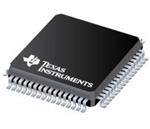
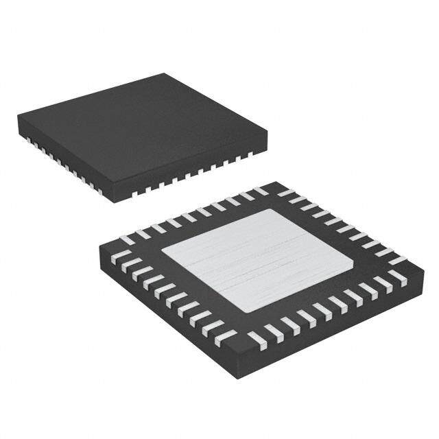
| 供应商器件封装 | 64-LQFP(10x10) |
| 其它名称 | 296-24724-1 |
| 制造商产品页 | http://www.ti.com/general/docs/suppproductinfo.tsp?distId=10&orderablePartNumber=MSP430FE425AIPMR |
| 包装 | 剪切带 (CT) |
| 外设 | 欠压检测/复位,LCD,POR,PWM,WDT |
| 封装/外壳 | 64-LQFP |
| 工作温度 | -40°C ~ 85°C |
| 振荡器类型 | 内部 |
| 数据转换器 | A/D 3x16b |
| 标准包装 | 1 |
| 核心处理器 | MSP430 |
| 核心尺寸 | 16-位 |
| 电压-电源(Vcc/Vdd) | 1.8 V ~ 3.6 V |
| 程序存储器类型 | 闪存 |
| 程序存储容量 | 16KB(16K x 8 + 256B) |
| 连接性 | SPI,UART/USART |
| 速度 | 8.4MHz |


PDF Datasheet 数据手册内容提取
MSP430FE42xA MIXED SIGNAL MICROCONTROLLER SLAS588--FEBRUARY2008 D LowSupply-VoltageRange,2.7Vto3.6V D BrownoutDetector D Ultra-LowPowerConsumption: D SupplyVoltageSupervisor/MonitorWith -- ActiveMode:400μAat1MHz,3.0V ProgrammableLevelDetection -- StandbyMode:1.6μA D SerialOnboardProgramming, -- OffMode(RAMRetention):0.1μA NoExternalProgrammingVoltageNeeded, D FivePower-SavingModes ProgrammableCodeProtectionbySecurity D Wake-UpFromStandbyModeinLess Fuse Than6μs D BootstrapLoaderinFlashDevices D Frequency-LockedLoop,FLL+ D FamilyMembersInclude: D 16-BitRISCArchitecture,125-ns -- MSP430FE423A: InstructionCycleTime 8KB+256BFlashMemory, 256BRAM D EmbeddedSignalProcessingfor -- MSP430FE425A: Single-PhaseEnergyMeteringWith 16KB+256BFlashMemory, IntegratedAnalogFront-Endand 512BRAM TemperatureSensor(ESP430CE1A) -- MSP430FE427A: D 16-BitTimer_AWithThree 32KB+256BFlashMemory, Capture/CompareRegisters 1KBRAM D IntegratedLCDDriverfor128Segments D Availablein64-PinQuadFlatPack(QFP) D SerialCommunicationInterface(USART), D ForCompleteModuleDescriptions,Refer AsynchronousUARTorSynchronousSPI totheMSP430x4xxFamilyUser’sGuide, SelectablebySoftware LiteratureNumberSLAU056 description TheTexasInstrumentsMSP430familyofultra-low-powermicrocontrollersconsistofseveraldevicesfeaturing differentsetsofperipheralstargetedforvariousapplications.Thearchitecture,combinedwithfivelowpower modes,isoptimizedtoachieveextendedbatterylifeinportablemeasurementapplications.Thedevicefeatures a powerful 16-bit RISC CPU, 16-bit registers, and constant generators that contribute to maximum code efficiency.Thedigitallycontrolledoscillator(DCO)allowswake-upfromlow-powermodestoactivemodeinless than6μs. TheMSP430FE42xAseriesaremicrocontrollerconfigurationswiththreeindependent16-bitsigma-deltaA/D convertersandembeddedsignalprocessorcoreusedtomeasureandcalculatesingle-phaseenergyinboth 2-wireand3-wireconfigurations.Alsoincludedareabuilt-in16-bittimer,128LCDsegmentdrivecapability,and 14I/Opins. Typical applications include 2-wire and 3-wire single-phase metering including tamper-resistant meter implementations. This integrated circuit can be damaged by ESD. Texas Instruments recommends that all integrated circuits be handled with appropriateprecautions.Failuretoobserveproperhandlingandinstallationprocedurescancausedamage.ESDdamagecanrange fromsubtleperformancedegradationtocompletedevicefailure.Precisionintegratedcircuitsmaybemoresusceptibletodamage becauseverysmallparametricchangescouldcausethedevicenottomeetitspublishedspecifications.Thesedeviceshavelimited built-inESDprotection. Please be aware that an important notice concerning availability, standard warranty, and use in critical applications of TexasInstrumentssemiconductorproductsanddisclaimerstheretoappearsattheendofthisdatasheet. PRODUCTION DATA information is current as of publication date. Copyright©2008TexasInstrumentsIncorporated ProductsconformtospecificationsperthetermsofTexasInstruments standardwarranty.Productionprocessingdoesnotnecessarilyinclude testingofallparameters. POSTOFFICEBOX655303•DALLAS,TEXAS75265 1
MSP430FE42xA MIXED SIGNAL MICROCONTROLLER SLAS588--FEBRUARY2008 AVAILABLEOPTIONS PACKAGEDDEVICES TA PLASTIC64-PINQFP (PM) MSP430FE423AIPM --40°Cto85°C MSP430FE425AIPM MSP430FE427AIPM pin designation† 0 3 K S N D0 D0 MCL S31 OUT/ SVSI UTX URX NMI CLK TDI TA0 TA0/ TA1/ SVS S29 VCCVSSVSS2.3/ 2.4/ 2.5/ ST/ CK MS DI/T DO/ 1.0/ 1.1/ 1.2/ 1.3/ 1.4/ A D AP P P R T T T T P P P P P 6463 6261 60 59 58 57 56 55 54 53 52 51 5049 DV 1 48 P1.5/TACLK/ACLK/S28 CC I1+ 2 47 P1.6/SIMO0/S27 I1-- 3 46 P1.7/SOMI0/S26 I2+ 4 45 P2.0/TA2/S25 I2-- 5 44 P2.1/UCLK0/S24 V1+ 6 43 R33 V1-- 7 42 R23 XIN 8 41 R13 MSP430FE42xA XOUT 9 40 R03 VREF 10 39 COM3 P2.2/STE0 11 38 COM2 S0 12 37 COM1 S1 13 36 COM0 S2 14 35 S23 S3 15 34 S22 S4 16 33 S21 17 18 19 20 21 22 23 24 25 26 27 28 29 30 31 32 5 6 7 8 9 0 1 2 3 4 5 6 7 8 9 0 S S S S S 1 1 1 1 1 1 1 1 1 1 2 S S S S S S S S S S S †Itisrecommendedtoshortunusedanaloginputpairsandconnectthemtoanalogground. 2 POSTOFFICEBOX655303•DALLAS,TEXAS75265
MSP430FE42xA MIXED SIGNAL MICROCONTROLLER SLAS588--FEBRUARY2008 functional block diagram XIN XOUT DVCC DVSS AVCC AVSS P1 P2 8 6 ACLK Oscillators Flash RAM Timer_A3 Port1 Port2 USART0 FLL+ SMCLK 32KB 1KB 3CCReg 8I/O 6I/O UARTor MCLK 16KB 512B Interrupt Interrupt SPI 8KB 256B Capability Capability Function MAB 8MHz CPU incl.16 Registers MDB EMmoudlautlieon PSOVSR// WWatcDhTd+og ESEPm4b3e0dCdEed1A TBimaesirc1 L1C2D8 Brownout Signal Segments 15/16-Bit Processing, 1Interrupt 1,2,3,4MUX JTAG Analog Vector Front-End Interface fLCD RST/NMI POSTOFFICEBOX655303•DALLAS,TEXAS75265 3
MSP430FE42xA MIXED SIGNAL MICROCONTROLLER SLAS588--FEBRUARY2008 Terminal Functions TERMINAL II//OO DDEESSCCRRIIPPTTIIOONN NAME NO. DVCC 1 Digitalsupplyvoltage,positiveterminal. I1+ 2 I Current1positiveanaloginput.InternalconnectiontoSD16Channel0A0+.(seeNote1) I1-- 3 I Current1negativeanaloginput. InternalconnectiontoSD16Channel0A0--.(seeNote1) I2+ 4 I Current2positiveanaloginput.InternalconnectiontoSD16Channel1A0+.(seeNote1) I2-- 5 I Current2negativeanaloginput.InternalconnectiontoSD16Channel1A0--.(seeNote1) V1+ 6 I Voltage1positiveanaloginput. InternalconnectiontoSD16Channel2A0+.(seeNote1) V1-- 7 I Voltage1negativeanaloginput.InternalconnectiontoSD16Channel2A0--.(seeNote1) XIN 8 I InputforcrystaloscillatorXT1.Standardorwatchcrystalscanbeconnected. XOUT 9 O OutputofcrystaloscillatorXT1 VREF 10 I/O Inputforanexternalreferencevoltage/internalreferencevoltageoutput(canbeusedasmid-voltage) P2.2/STE0 11 I/O General-purposedigitalI/O/slavetransmitenable—USART0/SPImode S0 12 O LCDsegmentoutput0 S1 13 O LCDsegmentoutput1 S2 14 O LCDsegmentoutput2 S3 15 O LCDsegmentoutput3 S4 16 O LCDsegmentoutput4 S5 17 O LCDsegmentoutput5 S6 18 O LCDsegmentoutput6 S7 19 O LCDsegmentoutput7 S8 20 O LCDsegmentoutput8 S9 21 O LCDsegmentoutput9 S10 22 O LCDsegmentoutput10 S11 23 O LCDsegmentoutput11 S12 24 O LCDsegmentoutput12 S13 25 O LCDsegmentoutput13 S14 26 O LCDsegmentoutput14 S15 27 O LCDsegmentoutput15 S16 28 O LCDsegmentoutput16 S17 29 O LCDsegmentoutput17 S18 30 O LCDsegmentoutput18 S19 31 O LCDsegmentoutput19 S20 32 O LCDsegmentoutput20 S21 33 O LCDsegmentoutput21 S22 34 O LCDsegmentoutput22 S23 35 O LCDsegmentoutput23 COM0 36 O CommonoutputCOM0--3areusedforLCDbackplanes. COM1 37 O CommonoutputCOM0--3areusedforLCDbackplanes. COM2 38 O CommonoutputCOM0--3areusedforLCDbackplanes. COM3 39 O CommonoutputCOM0--3areusedforLCDbackplanes. R03 40 I Inputoffourthpositive(lowest)analogLCDlevel(V5) NOTE1: Itisrecommendedtoshortunusedanaloginputpairsandconnectthemtoanalogground. 4 POSTOFFICEBOX655303•DALLAS,TEXAS75265
MSP430FE42xA MIXED SIGNAL MICROCONTROLLER SLAS588--FEBRUARY2008 Terminal Functions (Continued) TERMINAL II//OO DDEESSCCRRIIPPTTIIOONN NAME NO. R13 41 I InputofthirdmostpositiveanalogLCDlevel(V4orV3) R23 42 I InputofsecondmostpositiveanalogLCDlevel(V2) R33 43 O OutputofmostpositiveanalogLCDlevel(V1) General-purposedigitalI/O/externalclockinput-USART0/UARTorSPImode,clockoutput—USART0/SPI P2.1/UCLK0/S24 44 I/O mode/LCDsegmentoutput24(SeeNote1) General-purposedigitalI/O/Timer_ACapture:CCI2Ainput,Compare:Out2output/LCDsegmentoutput P2.0/TA2/S25 45 I/O 25(SeeNote1) General-purposedigitalI/O/slaveout/masterinofUSART0/SPImode/LCDsegmentoutput26 P1.7/SOMI0/S26 46 I/O (SeeNote1) General-purposedigitalI/O/slavein/masteroutofUSART0/SPImode/LCDsegmentoutput27 P1.6/SIMO0/S27 47 I/O (SeeNote1) P1.5/TACLK/ General-purposedigitalI/O/Timer_AandSD16clocksignalTACLKinput/ACLKoutput(dividedby1, 48 I/O ACLK/S28 2,4,or8)/LCDsegmentoutput28(SeeNote1) P1.4/S29 49 I/O General-purposedigitalI/O/LCDsegmentoutput29(SeeNote1) P1.3/SVSOUT/ 50 I/O General-purposedigitalI/O/SVS:outputofSVScomparator/LCDsegmentoutput30(SeeNote1) S30 General-purposedigitalI/O/Timer_A,Capture:CCI1A,CCI1Binput,Compare:Out1output/LCDsegment P1.2/TA1/S31 51 I/O output31(SeeNote1) General-purposedigitalI/O/Timer_A,Capture:CCI0Binput/MCLKoutput. P1.1/TA0/MCLK 52 I/O Note:TA0isonlyaninputonthispin/BSLreceive P1.0/TA0 53 I/O General-purposedigitalI/O/Timer_A,Capture:CCI0Ainput,Compare:Out0output/BSLtransmit TDO/TDI 54 I/O Testdataoutput.TDO/TDIdataoutputorprogrammingdatainputterminal. TDI/TCLK 55 I Testdatainputortestclockinput.ThedeviceprotectionfuseisconnectedtoTDI. TMS 56 I Testmodeselect.TMSisusedasaninputportfordeviceprogrammingandtest. TCK 57 I Testclock.TCKistheclockinputportfordeviceprogrammingandtest. RST/NMI 58 I Resetinputornonmaskableinterruptinputport P2.5/URXD0 59 I/O General-purposedigitalI/O/receivedatain—USART0/UARTmode P2.4/UTXD0 60 I/O General-purposedigitalI/O/transmitdataout—USART0/UARTmode P2.3/SVSIN 61 I/O General-purposedigitalI/O/Analoginputtobrownout,supplyvoltagesupervisor Analogsupplyvoltage,negativeterminal.SuppliesSD16,SVS,brownout,oscillator,andLCDresistive AVSS 62 dividercircuitry. DVSS 63 Digitalsupplyvoltage,negativeterminal. Analogsupplyvoltage,positiveterminal.SuppliesSD16, SVS,brownout, oscillator,and LCDresistive AVCC 64 dividercircuitry;mustnotpoweruppriortoDVCC. NOTE1: LCDfunctionselectedautomaticallywhenapplicableLCDmodulecontrolbitsareset,notwithPxSELbits. POSTOFFICEBOX655303•DALLAS,TEXAS75265 5
MSP430FE42xA MIXED SIGNAL MICROCONTROLLER SLAS588--FEBRUARY2008 short-form description CPU TheMSP430CPUhasa16-bitRISCarchitecture ProgramCounter PC/R0 that is highly transparent to the application. All operations,otherthanprogram-flowinstructions, StackPointer SP/R1 are performed as register operations in StatusRegister SR/CG1/R2 conjunction with seven addressing modes for source operand and four addressing modes for ConstantGenerator CG2/R3 destinationoperand. General-PurposeRegister R4 The CPU is integrated with 16 registers that provide reduced instruction execution time. The General-PurposeRegister R5 register-to-register operation execution time is onecycleoftheCPUclock. General-PurposeRegister R6 Fouroftheregisters,R0toR3,arededicatedas General-PurposeRegister R7 program counter, stack pointer, status register, and constant generator, respectively. The General-PurposeRegister R8 remaining registers are general-purpose registers. General-PurposeRegister R9 PeripheralsareconnectedtotheCPUusingdata, General-PurposeRegister R10 address,andcontrolbuses,andcanbehandled withallinstructions. General-PurposeRegister R11 instructionset General-PurposeRegister R12 Theinstructionsetconsistsof51instructionswith three formats and seven address modes. Each General-PurposeRegister R13 instruction can operate on word and byte data. Table1 shows examples of the three types of General-PurposeRegister R14 instructionformats;theaddressmodesarelisted General-PurposeRegister R15 inTable2. Table1.InstructionWordFormats Dualoperands,source-destination e.g,.ADD R4,R5 R4+R5------>R5 Singleoperands,destinationonly e.g.,CALL R8 PC---->(TOS),R8---->PC Relativejump,un/conditional e.g.,JNE Jump-on-equalbit=0 Table2.AddressModeDescriptions ADDRESSMODE S D SYNTAX EXAMPLE OPERATION D D Register MOVRs,Rd MOVR10,R11 R10 ---->R11 D D Indexed MOVX(Rn),Y(Rm) MOV2(R5),6(R6) M(2+R5)---->M(6+R6) D D Symbolic(PCrelative) MOVEDE,TONI M(EDE)---->M(TONI) D D Absolute MOV&MEM,&TCDAT M(MEM)---->M(TCDAT) D Indirect MOV@Rn,Y(Rm) MOV@R10,Tab(R6) M(R10)---->M(Tab+R6) Indirect D M(R10)---->R11 MOV@Rn+,Rm MOV@R10+,R11 autoincrement R10+2---->R10 D Immediate MOV#X,TONI MOV#45,TONI #45 ---->M(TONI) NOTE: S=source,D=destination 6 POSTOFFICEBOX655303•DALLAS,TEXAS75265
MSP430FE42xA MIXED SIGNAL MICROCONTROLLER SLAS588--FEBRUARY2008 operatingmodes TheMSP430hasoneactivemodeandfivesoftwareselectablelow-powermodesofoperation.Aninterrupt eventcanwakeupthedevicefromanyofthefivelow-powermodes,servicetherequest,andrestorebackto thelow-powermodeonreturnfromtheinterruptprogram. Thefollowingsixoperatingmodescanbeconfiguredbysoftware: D Activemode(AM) -- Allclocksareactive. D Low-powermode0(LPM0) -- CPUisdisabled. ACLKandSMCLKremainactive,MCLKisavailabletomodules. FLL+loopcontrolremainsactive. D Low-powermode1(LPM1) -- CPUisdisabled. ACLKandSMCLKremainactive,MCLKisavailabletomodules. FLL+loopcontrolisdisabled. D Low-powermode2(LPM2) -- CPUisdisabled. MCLK,FLL+loopcontrol,andDCOCLKaredisabled. DCOdcgeneratorremainsenabled. ACLKremainsactive. D Low-powermode3(LPM3) -- CPUisdisabled. MCLK,FLL+loopcontrol,andDCOCLKaredisabled. DCOdcgeneratorisdisabled. ACLKremainsactive. D Low-powermode4(LPM4) -- CPUisdisabled. ACLKisdisabled. MCLK,FLL+loopcontrol,andDCOCLKaredisabled. DCOdcgeneratorisdisabled. Crystaloscillatorisstopped. POSTOFFICEBOX655303•DALLAS,TEXAS75265 7
MSP430FE42xA MIXED SIGNAL MICROCONTROLLER SLAS588--FEBRUARY2008 interruptvectoraddresses Theinterruptvectorsandthepower-upstartingaddressarelocatedintheaddressrangeof0FFFFhto0FFE0h. Thevectorcontainsthe16-bitaddressoftheappropriateinterrupt-handlerinstructionsequence. INTERRUPTSOURCE INTERRUPTFLAG SYSTEMINTERRUPT WORDADDRESS PRIORITY Power-up WDTIFG Reset 0FFFEh 15,highest Externalreset KEYV Watchdog (seeNote1) Flashmemory PCout-of-range(seeNote4) NMI NMIIFG(seeNotes1and3) (Non)maskable Oscillatorfault OFIFG(seeNotes1and3) (Non)maskable 0FFFCh 14 Flashmemoryaccessviolation ACCVIFG(seeNotes1and3) (Non)maskable MBCTL_OUTxIFG, ESP430 MBCTL_INxIFG Maskable 0FFFAh 13 (seeNotes1and2) SD16CCTLxSD16OVIFG, SD16 SD16CCTLxSD16IFG Maskable 0FFF8h 12 (seeNotes1and2) 0FFF6h 11 Watchdogtimer WDTIFG Maskable 0FFF4h 10 USART0receive URXIFG0 Maskable 0FFF2h 9 USART0transmit UTXIFG0 Maskable 0FFF0h 8 0FFEEh 7 Timer_A3 TACCR0CCIFG(seeNote2) Maskable 0FFECh 6 TACCR1andTACCR2 Timer_A3 CCIFGs,andTACTLTAIFG Maskable 0FFEAh 5 (seeNotes1and2) P1IFG.0toP1IFG.7 I/OportP1(eightflags) Maskable 0FFE8h 4 (seeNotes1and2) 0FFE6h 3 0FFE4h 2 P2IFG.0toP2IFG.7 I/OportP2(eightflags) Maskable 0FFE2h 1 (seeNotes1and2) BasicTimer1 BTIFG Maskable 0FFE0h 0, lowest NOTES: 1. Multiplesourceflags 2. Interruptflagsarelocatedinthemodule. 3. (Non)maskable:theindividualinterrupt-enablebitcandisableaninterruptevent,butthegeneralinterrupt-enablecannot. 4. AresetisgeneratediftheCPUtriestofetchinstructionsfromwithinthemoduleregistermemoryaddressrange(0hto01FFh)or fromwithinunusedaddressranges(from0600hto0BFFh). 8 POSTOFFICEBOX655303•DALLAS,TEXAS75265
MSP430FE42xA MIXED SIGNAL MICROCONTROLLER SLAS588--FEBRUARY2008 special function registers Mostinterruptandmoduleenablebitsarecollectedintothelowestaddressspace.Specialfunctionregisterbits thatarenotallocatedtoafunctionalpurposearenotphysicallypresentinthedevice.Simplesoftwareaccess isprovidedwiththisarrangement. interrupt enable 1 and 2 Address 7 6 5 4 3 2 1 0 0h UTXIE0 URXIE0 ACCVIE NMIIE OFIE WDTIE rw–0 rw–0 rw–0 rw–0 rw–0 rw–0 WDTIE: Watchdogtimerinterruptenable.Inactiveifwatchdogmodeisselected.Activeifwatchdogtimer isconfiguredinintervaltimermode. OFIE: Oscillatorfaultinterruptenable NMIIE: Nonmaskableinterruptenable ACCVIE: Flashaccessviolationinterruptenable URXIE0: USART0:UARTandSPIreceiveinterruptenable UTXIE0: USART0:UARTandSPItransmitinterruptenable Address 7 6 5 4 3 2 1 0 1h BTIE rw-0 BTIE: BasicTimer1interruptenable interrupt flag register 1 and 2 Address 7 6 5 4 3 2 1 0 02h UTXIFG0 URXIFG0 NMIIFG OFIFG WDTIFG rw–1 rw–0 rw–0 rw–1 rw–(0) WDTIFG: Set on watchdog timer overflow (in watchdog mode) or security key violation. Reset on V CC poweruporaresetconditionattheRST/NMIpininresetmode. OFIFG: Flagsetonoscillatorfault NMIIFG: SetviaRST/NMIpin URXIFG0: USART0:UARTandSPIreceiveflag UTXIFG0: USART0:UARTandSPItransmitflag Address 7 6 5 4 3 2 1 0 3h BTIFG rw-0 BTIFG: BasicTimer1interruptflag POSTOFFICEBOX655303•DALLAS,TEXAS75265 9
MSP430FE42xA MIXED SIGNAL MICROCONTROLLER SLAS588--FEBRUARY2008 module enable registers 1 and 2 Address 7 6 5 4 3 2 1 0 UTXE0 URXE0 04h USPIE0 rw–0 rw–0 URXE0: USART0:UARTmodereceiveenable UTXE0: USART0:UARTmodetransmitenable USPIE0: USART0:SPImodetransmitandreceiveenable Address 7 6 5 4 3 2 1 0 05h Legend: rw--0,1: BitCanBeReadandWritten.ItIsResetorSetbyPUC. rw--(0,1): BitCanBeReadandWritten.ItIsResetorSetbyPOR. SFRBitNotPresentinDevice. memory organization MSP430FE423A MSP430FE425A MSP430FE427A Memory Size 8KB 16KB 32KB Interruptvector Flash 0FFFFhto0FFE0h 0FFFFhto0FFE0h 0FFFFhto0FFE0h Codememory Flash 0FFFFhto0E000h 0FFFFhto0C000h 0FFFFhto08000h Informationmemory Size 256Byte 256Byte 256Byte 010FFhto01000h 010FFhto01000h 010FFhto01000h Bootmemory Size 1kB 1kB 1kB 0FFFhto0C00h 0FFFhto0C00h 0FFFhto0C00h RAM Size 256Byte 512Byte 1KB 02FFhto0200h 03FFhto0200h 05FFhto0200h Peripherals 16-bit 01FFhto0100h 01FFhto0100h 01FFhto0100h 8-bit 0FFhto010h 0FFhto010h 0FFhto010h 8-bitSFR 0Fhto00h 0Fhto00h 0Fhto00h bootstrap loader (BSL) TheMSP430bootstraploader(BSL)enablesuserstoprogramtheflashmemoryorRAMusingaUARTserial interface.AccesstotheMSP430memoryviatheBSLis protectedbyuser-definedpassword.Forcomplete descriptionofthefeaturesoftheBSLanditsimplementation,seetheApplicationreportFeaturesoftheMSP430 BootstrapLoader,LiteratureNumberSLAA089. BSLFUNCTION PMPACKAGEPINS Datatransmit 53-P1.0 Datareceive 52-P1.1 10 POSTOFFICEBOX655303•DALLAS,TEXAS75265
MSP430FE42xA MIXED SIGNAL MICROCONTROLLER SLAS588--FEBRUARY2008 flash memory TheflashmemorycanbeprogrammedviatheJTAGport,thebootstraploader,orin-systembytheCPU.The CPUcanperformsingle-byteandsingle-wordwritestotheflashmemory.Featuresoftheflashmemoryinclude: D Flashmemoryhasnsegmentsofmainmemoryandtwosegmentsofinformationmemory(AandB)of128 byteseach.Eachsegmentinmainmemoryis512bytesinsize. D Segments0tonmaybeerasedinonestep,oreachsegmentmaybeindividuallyerased. D SegmentsAandBcanbeerasedindividually,orasagroupwithsegments0ton. SegmentsAandBarealsocalledinformationmemory. D New devices may have some bytes programmed in the information memory (needed for test during manufacturing).Theusershouldperformaneraseoftheinformationmemorypriortothefirstuse. 8KB 16KB 32KB 0FFFFh 0FFFFh 0FFFFh Segment0 WithInterruptVectors 0FE00h 0FE00h 0FE00h 0FDFFh 0FDFFh 0FDFFh Segment1 0FC00h 0FC00h 0FC00h 0FBFFh 0FBFFh 0FBFFh Segment2 0FA00h 0FA00h 0FA00h 0F9FFh 0F9FFh 0F9FFh MainMemory 0E400h 0C400h 08400h 0E3FFh 0C3FFh 083FFh Segmentn--1 0E200h 0C200h 08200h 0E1FFh 0C1FFh 081FFh Segmentn 0E000h 0C000h 08000h 010FFh 010FFh 010FFh SegmentA 01080h 01080h 01080h InformationMemory 0107Fh 0107Fh 0107Fh SegmentB 01000h 01000h 01000h POSTOFFICEBOX655303•DALLAS,TEXAS75265 11
MSP430FE42xA MIXED SIGNAL MICROCONTROLLER SLAS588--FEBRUARY2008 peripherals PeripheralsareconnectedtotheCPUthroughdata,address,andcontrolbussesandcanbehandledusing all instructions. For complete module descriptions, refer to the MSP430x4xx Family User’s Guide, literature numberSLAU056. oscillator and system clock The clock system in the MSP430FE42xA family of devices is supported by the FLL+ module that includes support for a 32768-Hz watch crystal oscillator, an internal digitally-controlled oscillator (DCO) and a high-frequency crystal oscillator. The FLL+ clock module is designed to meet the requirements of both low systemcostandlowpowerconsumption.TheFLL+featuresadigitalfrequencylockedloop(FLL)hardware that,inconjunctionwithadigitalmodulator,stabilizestheDCOfrequencytoaprogrammablemultipleofthe watchcrystalfrequency.TheinternalDCOprovidesafastturn-onclocksourceandstabilizesinlessthan6μs. TheFLL+moduleprovidesthefollowingclocksignals: D Auxiliaryclock(ACLK),sourcedfroma32768-Hzwatchcrystalorahigh-frequencycrystal. D Mainclock(MCLK),thesystemclockusedbytheCPU. D Sub-Mainclock(SMCLK),thesub-systemclockusedbytheperipheralmodules. D ACLK/n,thebufferedoutputofACLK,ACLK/2,ACLK/4,orACLK/8. brownout, supply voltage supervisor (SVS) Thebrownoutcircuitisimplementedtoprovidetheproperinternalresetsignaltothedeviceduringpoweron andpoweroff.TheSVScircuitrydetectsifthesupplyvoltagedropsbelowauserselectablelevelandsupports bothsupplyvoltagesupervision(thedeviceisautomaticallyreset)andsupplyvoltagemonitoring(SVM)(the deviceisnotautomaticallyreset). TheCPUbeginscodeexecutionafterthebrownoutcircuitreleasesthedevicereset.However,V maynot CC haverampedtoV atthattime.TheusermustensurethedefaultFLL+settingsarenotchangeduntilV CC(min) CC reachesV .Ifdesired,theSVScircuitcanbeusedtodeterminewhenV reachesV . CC(min) CC CC(min) digital I/O Therearetwo8-bitI/Oportsimplemented—portsP1andP2(onlysixP2I/Osignalsareavailableonexternal pins): D AllindividualI/Obitsareindependentlyprogrammable. D Anycombinationofinput,output,andinterruptconditionsispossible. D Edge-selectableinterruptinputcapabilityforalltheeightbitsofportP1andsixbitsofP2. D Read/writeaccesstoport-controlregistersissupportedbyallinstructions. NOTE: SixbitsofportP2,P2.0toP2.5,areavailableonexternalpins-butallcontrolanddatabitsforport P2areimplemented. Basic Timer1 TheBasicTimer1hastwoindependent8-bittimersthatcanbecascadedtoforma16-bittimer/counter.Both timerscanbereadandwrittenbysoftware.TheBasicTimer1canbeusedtogenerateperiodicinterruptsand clockfortheLCDmodule. LCD drive The LCD driver generates the segment and common signals required to drive an LCD display. The LCD controllerhasdedicateddatamemorytoholdsegmentdriveinformation.Commonandsegmentsignalsare generatedasdefinedbythemode.Static,2-MUX,3-MUX,and4-MUXLCDsaresupportedbythisperipheral. 12 POSTOFFICEBOX655303•DALLAS,TEXAS75265
MSP430FE42xA MIXED SIGNAL MICROCONTROLLER SLAS588--FEBRUARY2008 WDT+ watchdog timer The primary functionofthewatchdog timer(WDT+) moduleis toperformacontrolled systemrestartaftera software problem occurs. If the selected time interval expires, a system reset is generated. If the watchdog functionisnotneededinanapplication,themodulecanbeconfiguredasanintervaltimerandcangenerate interruptsatselectedtimeintervals. Timer_A3 Timer_A3 is a 16-bit timer/counter with three capture/compare registers. Timer_A3 can support multiple capture/compares, PWM outputs, and interval timing. Timer_A3 also has extensive interrupt capabilities. Interruptsmaybegeneratedfromthecounteronoverflowconditionsandfromeachofthecapture/compare registers. TIMER_A3SIGNALCONNECTIONS INPUTPIN DEVICEINPUT MODULEINPUT MODULEOUTPUT OUTPUTPIN MODULEBLOCK NUMBER SIGNAL NAME SIGNAL NUMBER 48-P1.5 TACLK TACLK ACLK ACLK TTiimmeerr NNAA SMCLK SMCLK 48-P1.5 TACLK INCLK 53-P1.0 TA0 CCI0A 53-P1.0 52-P1.1 TA0 CCI0B CCCCRR00 TTAA00 DVSS GND DVCC VCC 51-P1.2 TA1 CCI1A 51-P1.2 51-P1.2 TA1 CCI1B CCCCRR11 TTAA11 DVSS GND DVCC VCC 45-P2.0 TA2 CCI2A 45-P2.0 ACLK(internal) CCI2B CCCCRR22 TTAA22 DVSS GND DVCC VCC universal synchronous/asynchronous receive transmit (USART) TheMSP430FE42xAdeviceshaveonehardwareUSARTperipheralmodule(USART0)thatisusedforserial data communication. The USART supports synchronous SPI (3 or 4 pin) and asynchronous UART communicationprotocols,usingdouble-bufferedtransmitandreceivechannels. ESP430CE1A The ESP430CE1A module integrates a hardware multiplier, three independent 16-bit sigma-delta A/D converters(SD16)andanembeddedsignalprocessor(ESP430).TheESP430CE1Amodulemeasures2-wire or3-wiresingle-phaseenergyandautomaticallycalculatesparametersthataremadeavailabletotheMSP430 CPU.Themodulecanbecalibratedandinitializedtoaccuratelycalculateenergy,powerfactor,etc.,forawide rangeofmeteringsensorconfigurations. POSTOFFICEBOX655303•DALLAS,TEXAS75265 13
MSP430FE42xA MIXED SIGNAL MICROCONTROLLER SLAS588--FEBRUARY2008 peripheral file map PERIPHERALSWITHWORDACCESS Watchdog Watchdogtimercontrol WDTCTL 0120h Timer__A3 Timer_Ainterruptvector TAIV 012Eh Timer_Acontrol TACTL 0160h Capture/comparecontrol0 TACCTL0 0162h Capture/comparecontrol1 TACCTL1 0164h Capture/comparecontrol2 TACCTL2 0166h Reserved 0168h Reserved 016Ah Reserved 016Ch Reserved 016Eh Timer_Aregister TAR 0170h Capture/compareregister0 TACCR0 0172h Capture/compareregister1 TACCR1 0174h Capture/compareregister2 TACCR2 0176h Reserved 0178h Reserved 017Ah Reserved 017Ch Reserved 017Eh HardwareMultipplier Sumextend SUMEXT 013Eh (seeNote1) Resulthighword RESHI 013Ch Resultlowword RESLO 013Ah Secondoperand OP2 0138h Multiplysigned+accumulate/operand1 MACS 0136h Multiply+accumulate/operand1 MAC 0134h Multiplysigned/operand1 MPYS 0132h Multiplyunsigned/operand1 MPY 0130h Flash Flashcontrol3 FCTL3 012Ch Flashcontrol2 FCTL2 012Ah Flashcontrol1 FCTL1 0128h SD16((seeNote1)) Generalcontrol SD16CTL 0100h (see also: Peripherals Channel0control SD16CCTL0 0102h WWiitthhBByytteeAAcccceessss)) Channel1control SD16CCTL1 0104h Channel2control SD16CCTL2 0106h Reserved 0108h Reserved 010Ah Reserved 010Ch Reserved 010Eh Interruptvectorwordregister SD16IV 0110h Channel0conversionmemory SD16MEM0 0112h NOTE1: ModuleiscontainedwithinESP430CE1A.RegistersnotaccessiblewhenESP430isactive.ESP430mustbedisabledorsuspended toallowCPUaccesstothesemodules. 14 POSTOFFICEBOX655303•DALLAS,TEXAS75265
MSP430FE42xA MIXED SIGNAL MICROCONTROLLER SLAS588--FEBRUARY2008 peripheral file map (continued) PERIPHERALSWITHWORDACCESS SD16 Channel1conversionmemory SD16MEM1 0114h (continued,seeNote1) Channel2conversionmemory SD16MEM2 0116h Reserved 0118h Reserved 011Ah Reserved 011Ch Reserved 011Eh ESP430((ESP430CE1A)) ESP430control ESPCTL 0150h Mailboxcontrol MBCTL 0152h Mailboxin0 MBIN0 0154h Mailboxin1 MBIN1 0156h Mailboxout0 MBOUT0 0158h Mailboxout1 MBOUT1 015Ah ESP430returnvalue0 RET0 01C0h : : : ESP430returnvalue31 RET31 01FEh PERIPHERALSWITHBYTEACCESS SD16((seeNote1)) Channel0inputcontrol SD16INCTL0 0B0h (see also: Peripherals Channel1inputcontrol SD16INCTL1 0B1h WWiitthhWWoorrddAAcccceessss)) Channel2inputcontrol SD16INCTL2 0B2h Reserved 0B3h Reserved 0B4h Reserved 0B5h Reserved 0B6h Reserved 0B7h Channel0preload SD16PRE0 0B8h Channel1preload SD16PRE1 0B9h Channel2preload SD16PRE2 0BAh Reserved 0BBh Reserved 0BCh Reserved 0BDh Reserved 0BEh Reserved 0BFh LCD LCDmemory20 LCDM20 0A4h : : : LCDmemory16 LCDM16 0A0h LCDmemory15 LCDM15 09Fh : : : LCDmemory1 LCDM1 091h LCDcontrolandmode LCDCTL 090h NOTE1: ModuleiscontainedwithinESP430CE1A.RegistersnotaccessiblewhenESP430isactive.ESP430mustbedisabledorsuspended toallowCPUaccesstothesemodules. POSTOFFICEBOX655303•DALLAS,TEXAS75265 15
MSP430FE42xA MIXED SIGNAL MICROCONTROLLER SLAS588--FEBRUARY2008 peripheral file map (continued) PERIPHERALSWITHBYTEACCESS(CONTINUED) USART0 Transmitbuffer U0TXBUF 077h Receivebuffer U0RXBUF 076h Baudrate U0BR1 075h Baudrate U0BR0 074h Modulationcontrol U0MCTL 073h Receivecontrol U0RCTL 072h Transmitcontrol U0TCTL 071h USARTcontrol U0CTL 070h Brownout,SVS SVScontrolregister SVSCTL 056h FLL+Clock FLL+control1 FLL_CTL1 054h FLL+control0 FLL_CTL0 053h Systemclockfrequencycontrol SCFQCTL 052h Systemclockfrequencyintegrator SCFI1 051h Systemclockfrequencyintegrator SCFI0 050h BasicTimer1 BTcounter2 BTCNT2 047h BTcounter1 BTCNT1 046h BTcontrol BTCTL 040h PortP2 PortP2selection P2SEL 02Eh PortP2interruptenable P2IE 02Dh PortP2interrupt-edgeselect P2IES 02Ch PortP2interruptflag P2IFG 02Bh PortP2direction P2DIR 02Ah PortP2output P2OUT 029h PortP2input P2IN 028h PortP1 PortP1selection P1SEL 026h PortP1interruptenable P1IE 025h PortP1interrupt-edgeselect P1IES 024h PortP1interruptflag P1IFG 023h PortP1direction P1DIR 022h PortP1output P1OUT 021h PortP1input P1IN 020h SppecialFunctions SFRmoduleenable2 ME2 005h SFRmoduleenable1 ME1 004h SFRinterruptflag2 IFG2 003h SFRinterruptflag1 IFG1 002h SFRinterruptenable2 IE2 001h SFRinterruptenable1 IE1 000h 16 POSTOFFICEBOX655303•DALLAS,TEXAS75265
MSP430FE42xA MIXED SIGNAL MICROCONTROLLER SLAS588--FEBRUARY2008 absolute maximum ratings† VoltageappliedatV toV .................................................... --0.3Vto+4.1V CC SS Voltageappliedtoanypin(seeNote1) ....................................... --0.3VtoV +0.3V CC Diodecurrentatanydeviceterminal ...................................................... ±2mA Storagetemperature(unprogrammeddevice) ...................................... --55°Cto150°C Storagetemperature(programmeddevice) ......................................... --40°Cto85°C †Stressesbeyondthoselistedunder“absolutemaximumratings”maycausepermanentdamagetothedevice.Thesearestressratingsonly,and functionaloperationofthedeviceattheseoranyotherconditionsbeyondthoseindicatedunder“recommendedoperatingconditions”isnot implied.Exposuretoabsolute-maximum-ratedconditionsforextendedperiodsmayaffectdevicereliability. NOTE1: AllvoltagesreferencedtoVSS.TheJTAGfuse-blowvoltage,VFB,isallowedtoexceedtheabsolutemaximumrating.Thevoltageis appliedtotheTDI/TCLKpinwhenblowingtheJTAGfuse. recommended operating conditions (see Note 1) PARAMETER MIN NOM MAX UNITS Supplyvoltageduringprogramexecution;ESP430andSD16disabled, MSP430FE42xA 1.8 3.6 V VCC(AVCC=DVCC=VCC)(seeNote1) Supplyvoltageduringprogramexecution;SVSenabled,PORON=1, ESP430andSD16disabled,VCC(AVCC=DVCC=VCC) MSP430FE42xA 2.0 3.6 V (seeNotes1and2) Supplyvoltageduringprogramexecution;ESP430orSD16enabledor duringprogrammingofflashmemory,VCC(AVCC=DVCC=VCC) MSP430FE42xA 2.7 3.6 V (seeNote1) Supplyvoltage(seeNote1),VSS(AVSS=DVSS=VSS) 0 0 V Operatingfree-airtemperaturerange,TA MSP430FE42xA --40 85 °C LFselected,XTS_FLL=0 Watchcrystal 32768 Hz LLFFXXTT11ccrryyssttaallffrreeqquueennccyy,,ff((LLFFXXTT11))((sseeeeNNoottee33)) XT1selected,XTS_FLL=1 Ceramicresonator 450 8000 kHz XT1selected,XTS_FLL=1 Crystal 1000 8000 kHz VCC=2.7V DC 8.4 PPrroocceessssoorrffrreeqquueennccyy((ssiiggnnaallMMCCLLKK)),ff(System)((sseeeeNNoottee44)) VCC=3.6V DC 8.4 MMHHzz NOTES: 1. ItisrecommendedtopowerAVCCandDVCCfromthesamesource.Amaximumdifferenceof0.3Vbetween AVCCandDVCCcan betoleratedduringpowerupandoperation. 2. TheminimumoperatingsupplyvoltageisdefinedaccordingtothetrippointwherePORisgoingactivebydecreasingsupplyvoltage. PORisgoinginactivewhenthesupplyvoltageisraisedaboveminimumsupplyvoltageplusthehysteresisoftheSVScircuitry. 3. TheLFXT1oscillatorinLF-moderequiresawatchcrystal. 4. Forfrequenciesabove8MHz,MCLKissourcedbythebuilt-inoscillator(DCOandFLL+). POSTOFFICEBOX655303•DALLAS,TEXAS75265 17
MSP430FE42xA MIXED SIGNAL MICROCONTROLLER SLAS588--FEBRUARY2008 electrical characteristics over recommended operating free-air temperature (unless otherwise noted) supplycurrentintoAV +DV excludingexternalcurrent(seeNote1) CC CC PARAMETER TESTCONDITIONS VCC MIN NOM MAX UNIT Activemode, f(MCLK)=f(SMCLK)=f(DCO)=1MHz, I(AM) f(ACLK)=32,768Hz,XTS_FLL=0 TA=--40°Cto85°C 3V 400 500 μA (programexecutesinflash) Low-powermode,(LPM0/LPM1) f(MCLK)=f(SMCLK)=f(DCO)=1MHz, I(LPM0) f(ACLK)=32,768Hz,XTS_FLL=0 TA=--40°Cto85°C 3V 130 150 μA FN_8=FN_4=FN_3=FN_2=0(seeNote2) I(LPM2) Low-powermode,(LPM2)(seeNote2) TA=--40°Cto85°C 3V 10 22 μA TA=--40°C 1.5 2.0 TA=25°C 1.6 2.1 II(LPM3) LLooww-ppoowweerrmmooddee,((LLPPMM33))((sseeeeNNoottee22)) 33VV μAA TA=60°C 1.7 2.2 TA=85°C 2.0 3.5 TA=--40°C 0.1 0.5 II((LLPPMM44)) LLooww-ppoowweerrmmooddee,,((LLPPMM44))((sseeeeNNoottee22)) TA=25°C 33VV 0.1 0.5 μμAA TA=85°C 0.8 2.5 NOTES: 1. Allinputsaretiedto0VorVCC.Outputsdonotsourceorsinkanycurrent. ThecurrentconsumptioninLPM2,LPM3,andLPM4aremeasuredwithactiveBasicTimer1andLCD(ACLKselected). ThecurrentconsumptionoftheESP430CE1AandtheSVSmodulearespecifiedintheirrespectivesections. LPMxcurrentsmeasuredwithWDT+disabled. ThecurrentsarecharacterizedwithaKDSDaishinkuDT--38(6pF)crystal. 2. Currentforbrownoutincluded. current consumption of active mode versus system frequency I =I ×f (AM) (AM)[1MHz] (System)[MHz] current consumption of active mode versus supply voltage I =I +170μA/V×(V –3V) (AM) (AM)[3V] CC f(MHz) SupplyVoltageRangewith z H ESP430orSD16EnabledandDuring M -- ProgrammingoftheFlashMemory y 8.4MHz c n SupplyVoltageRange e u DuringProgram q e Execution r F 6MHz r o s s e c ro 4.15MHz P m u m xi a M -- m e st y S f 1.8V 2.7V 3V 3.6V VCC--SupplyVoltage--V Figure1.FrequencyvsSupplyVoltage 18 POSTOFFICEBOX655303•DALLAS,TEXAS75265
MSP430FE42xA MIXED SIGNAL MICROCONTROLLER SLAS588--FEBRUARY2008 electrical characteristics over recommended operating free-air temperature (unless otherwise noted) (continued) Schmitt-triggerinputs -- PortsP1andP2,RST/NMI,JTAG(TCK,TMS,TDI/TCLK,TDO/TDI) PARAMETER VCC MIN TYP MAX UNIT VIT+ Positive-goinginputthresholdvoltage 3V 1.5 1.98 V VIT-- Negative-goinginputthresholdvoltage 3V 0.9 1.3 V Vhys Inputvoltagehysteresis(VIT+--VIT--) 3V 0.45 1 V inputsPx.x,TAx PARAMETER TESTCONDITIONS VCC MIN TYP MAX UNIT PPoorrttPP11,,PP22::PP11..xxttooPP22..xx,,EExxtteerrnnaallttrriiggggeerrssiiggnnaall 3V 1.5 cycle tt(int) EExxtteerrnnaalliinntteerrrruuppttttiimmiinngg fortheinterruptflag(seeNote1) 3V 50 ns t(cap) Timer_A,capturetiming TAx 3V 50 ns Timer_Aclockfrequency f(TAext) externallyappliedtopin TACLK,INCLKt(H)=t(L) 3V 10 MHz f(TAint) Timer_Aclockfrequency SMCLKorACLKsignalselected 3V 10 MHz NOTES: 1. Theexternalsignalsetstheinterruptflageverytimetheminimumt(int)cycleandtimeparametersaremet.Itmaybesetevenwith triggersignalsshorterthant(int).Boththecycleandtimingspecificationsmustbemettoensuretheflagisset.t(int)ismeasuredin MCLKcycles. leakagecurrent(seeNote1) PARAMETER TESTCONDITIONS VCC MIN NOM MAX UNIT Ilkg(P1.x) PortP1 Port1:V(P1.x)(seeNote2) ±50 LLeeaakkaaggeeccuurrrreenntt 33VV nnAA Ilkg(P2.x) PortP2 Port2:V(P2.x)(seeNote2) ±50 NOTES: 1. TheleakagecurrentismeasuredwithVSSorVCCappliedtothecorrespondingpin(s),unlessotherwisenoted. 2. Theportpinmustbeselectedasaninput. outputs -- PortsP1andP2 PARAMETER TESTCONDITIONS VCC MIN TYP MAX UNIT IOH(max)=--1.5mA(seeNote1) VCC--0.25 VCC VVOH HHiigghh-lleevveelloouuttppuuttvvoollttaaggee 33VV VV IOH(max)=--6mA(seeNote2) VCC--0.6 VCC IOL(max)=1.5mA(seeNote1) VSS VSS+0.25 VVOL LLooww-lleevveelloouuttppuuttvvoollttaaggee 33VV VV IOL(max)=6mA(seeNote2) VSS VSS+0.6 NOTES: 1. Themaximumtotalcurrent,IOH(max)andIOL(max),foralloutputscombined,shouldnotexceed±12mAtosatisfythe maximumspecifiedvoltagedrop. 2. Themaximumtotalcurrent,IOH(max)andIOL(max),foralloutputscombined,shouldnotexceed±48mAtosatisfythe maximumspecifiedvoltagedrop. outputfrequency PARAMETER TESTCONDITIONS VCC MIN TYP MAX UNIT fPx.y (1≤x≤2, 0≤y≤7) CILL==±210.5pmF,A 3V dc 12 MHz fACLK, P1.1/TA0/MCLK fMCLK, P1.5/TACLK/ACLK/S28 CL=20pF 3V 12 MHz fSMCLK fACLK=fLFXT1=fXT1 40% 60% PP11.55//TTAACCLLKK//AACCLLKK//SS2288, DDuuttyyccyycclleeooffoouuttppuutt CCLL==2200ppFF fACLK=fLFXT1=fLF 30% 70% tXXddcc ffrreeqquueennccyy fACLK=fLFXT1 3V 50% P1.1/TA0/MCLK, 50%-- 50%+ CL=20pF fMCLK=fDCOCLK 15ns 50% 15ns POSTOFFICEBOX655303•DALLAS,TEXAS75265 19
MSP430FE42xA MIXED SIGNAL MICROCONTROLLER SLAS588--FEBRUARY2008 electrical characteristics over recommended operating free-air temperature (unless otherwise noted) (continued) outputs -- PortsP1andP2(continued) TYPICALLOW-LEVELOUTPUTCURRENT TYPICALLOW-LEVELOUTPUTCURRENT vs vs LOW-LEVELOUTPUTVOLTAGE LOW-LEVELOUTPUTVOLTAGE 30 50 A VCC=2.2V VCC=3V m P2.1 TA=25°C mA P2.1 TA=25°C -- 25 ent nt-- 40 r e Cur 20 TA=85°C Curr TA=85°C put ut 30 Out utp vel 15 elO e v Low-l 10 ow-le 20 cal alL ypi pic 10 T 5 y T -- L -- O L O I 0 I 0 0.0 0.5 1.0 1.5 2.0 2.5 0.0 0.5 1.0 1.5 2.0 2.5 3.0 3.5 VOL--Low-LevelOutputVoltage--V VOL--Low-LevelOutputVoltage--V Figure2 Figure3 TYPICALHIGH-LEVELOUTPUTCURRENT TYPICALHIGH-LEVELOUTPUTCURRENT vs vs HIGH-LEVELOUTPUTVOLTAGE HIGH-LEVELOUTPUTVOLTAGE 0 0 A VP2C.C1=2.2V VCC=3V m A P2.1 -- --5 m rrent ent-- --10 u r C --10 ur ut C utp put --20 O ut el --15 O picalHigh-lev --20 TA=85°C calHigh-level --30 TA=85°C Ty --25 TA=25°C ypi --40 -- T OL --L I --30 IO --50 TA=25°C 0.0 0.5 1.0 1.5 2.0 2.5 0.0 0.5 1.0 1.5 2.0 2.5 3.0 3.5 VOH--High-LevelOutputVoltage--V VOH--High-LevelOutputVoltage--V Figure4 Figure5 NOTEA. Oneoutputloadedatatime 20 POSTOFFICEBOX655303•DALLAS,TEXAS75265
MSP430FE42xA MIXED SIGNAL MICROCONTROLLER SLAS588--FEBRUARY2008 electrical characteristics over recommended operating free-air temperature (unless otherwise noted) (continued) wake-upLPM3 PARAMETER TESTCONDITIONS VCC MIN TYP MAX UNIT f=1MHz 6 ttdd((LLPPMM33)) DDeellaayyttiimmee f=2MHz 33VV 6 μμss f=3MHz 6 RAM(seeNote1) PARAMETER TESTCONDITIONS MIN TYP MAX UNIT VRAMh CPUhalted(seeNote1) 1.6 V NOTE1: ThisparameterdefinestheminimumsupplyvoltagewhenthedataintheprogrammemoryRAMremainunchanged.Noprogram executionshouldtakeplaceduringthissupplyvoltagecondition. LCD PARAMETER TESTCONDITIONS MIN TYP MAX UNIT V(33) VoltageatR33 2.5 VCC+0.2 V(23) VoltageatR23 (V33--V03)×2/3+V03 AAnnaallooggvvoollttaaggee VVCC=33VV VV V(13) VoltageatR13 (V(33)--V(03))×1/3+V(03) V(33)--V(03) VoltageatR33/R03 2.5 VCC+0.2 I(R03) R03=VSS Noloadatall ±20 segmentand I(R13) Inpputleakagge R13=VCC/3 ±20 nA ccoommmmoonnlliinneess, I(R23) R23=2×VCC/3 VCC=3V ±20 V(Sxx0) V(03) V(03)--0.1 V(Sxx1) SSeeggmmeennttlliinnee V(13) V(13)--0.1 V(Sxx2) voltage II(Sxx)=--33μAA, VVCC=33VV V(23) V(23)--0.1 VV V(Sxx3) V(33) V(33)+0.1 USART0(seeNote1) PARAMETER TESTCONDITIONS MIN NOM MAX UNIT t(τ) USART0:deglitchtime VCC=3V,SYNC=0,UARTmode 150 280 500 ns NOTE1: ThesignalappliedtotheUSART0receivesignal/terminal(URXD0)shouldmeetthetimingrequirementsoft(τ)toensurethattheURXS flip-flopisset.TheURXSflip-flopissetwithnegativepulsesmeetingtheminimum-timingconditionoft(τ).Theoperatingconditionsto settheflagmustbemetindependentlyfromthistimingconstraint.Thedeglitchcircuitryisactiveonlyonnegativetransitionsonthe URXD0line. PORbrownout,reset(seeNotes1and2) PARAMETER TESTCONDITIONS MIN TYP MAX UNIT td(BOR) 2000 μs VCC(start) dVCC/dt≤3V/s(seeFigure6) 0.7×V(B_IT--) V V(B_IT--) BBrroowwnnoouutt dVCC/dt≤3V/s(seeFigure6,Figure7,Figure8) 1.71 V Vhys(B_IT--) dVCC/dt≤3V/s(seeFigure6) 70 130 180 mV PulselengthneededatRST/NMIpintoacceptedresetinternally, t(reset) VCC=3V 2 μs NOTES: 1. ThecurrentconsumptionofthebrownoutmoduleisalreadyincludedintheICCcurrentconsumptiondata.ThevoltagelevelV(B_IT--) +Vhys(B_IT--)is≤1.8V. 2. Duringpowerup,theCPUbeginscodeexecutionfollowingaperiodoftd(BOR)afterVCC=V(B_IT--)+Vhys(B_IT--). ThedefaultFLL+settingsmustnotbechangeduntilVCC≥VCC(min),whereVCC(min)istheminimumsupplyvoltageforthedesired operatingfrequency.SeetheMSP430x4xxFamilyUser’sGuide(SLAU056)formoreinformationonthebrownout/SVScircuit. POSTOFFICEBOX655303•DALLAS,TEXAS75265 21
MSP430FE42xA MIXED SIGNAL MICROCONTROLLER SLAS588--FEBRUARY2008 electrical characteristics over recommended operating free-air temperature (unless otherwise noted) (continued) VCC Vhys(B_IT--) V(B_IT--) VCC(start) 1 0 td(BOR) Figure6.POR/BrownoutReset(BOR)vsSupplyVoltage 2 VCC tpw V =3V 3V cc TypicalConditions 1.5 V -- p) o 1 r d ( CC VCC(drop) V 0.5 0 0.001 1 1000 1ns 1ns tpw--PulseWidth--μs tpw--PulseWidth--μs Figure7.V LevelWithaSquareVoltageDroptoGenerateaPOR/BrownoutSignal CC(drop) VCC tpw 2 3V V =3V cc 1.5 TypicalConditions V -- p) o 1 r d (C VCC(drop) C 0.5 V tf=tr 0 0.001 1 1000 tf tr tpw--PulseWidth--μs tpw--PulseWidth--μs Figure8.V LevelWithaTriangleVoltageDroptoGenerateaPOR/BrownoutSignal CC(drop) 22 POSTOFFICEBOX655303•DALLAS,TEXAS75265
MSP430FE42xA MIXED SIGNAL MICROCONTROLLER SLAS588--FEBRUARY2008 electrical characteristics over recommended operating free-air temperature (unless otherwise noted) (continued) SVS(supplyvoltagesupervisor/monitor)(seeNote1) PARAMETER TESTCONDITIONS MIN NOM MAX UNIT dVCC/dt>30V/ms(seeFigure9) 5 150 tt(SVSR)4 μμss dVCC/dt≤30V/ms 2000 td(SVSon) SVSon,switchfromVLD=0toVLD≠0,VCC=3V 20 150 μs tsettle VLD≠0‡ 12 μs V(SVSstart) VLD≠0,VCC/dt≤3V/s(seeFigure9) 1.55 1.7 V VLD=1 70 120 155 mV VCC/dt≤3V/s(seeFigure9) VLD=2to14 V(SVS_IT--) V(SVS_IT--) VVhhyyss((SSVVSS_IITT----)) x0.001 x0.016 VCC/dt≤3V/s(seeFigure9),externalvoltageapplied VLD=15 1 20 mV onP2.3 VLD=1 1.8 1.9 2.05 VLD=2 1.94 2.1 2.25 VLD=3 2.05 2.2 2.37 VLD=4 2.14 2.3 2.48 VLD=5 2.24 2.4 2.6 VLD=6 2.33 2.5 2.71 VLD=7 2.46 2.65 2.86 VVCC//ddtt≤≤33VV//ss((sseeeeFFiigguurree99)) VLD=8 2.58 2.8 3 VV((SSVVSS_IITT--)) VV VLD=9 2.69 2.9 3.13 VLD=10 2.83 3.05 3.29 VLD=11 2.94 3.2 3.42 VLD=12 3.11 3.35 3.61† VLD=13 3.24 3.5 3.76† VLD=14 3.43 3.7† 3.99† VCC/dt≤3V/s(seeFigure9),externalvoltageapplied VLD=15 1.1 1.2 1.3 onP2.3 I(CseCe(SNVSo)te1) VLD≠0,VCC=2.2V/3V 10 15 μA †Therecommendedoperatingvoltagerangeislimitedto3.6V. ‡tsettleisthesettlingtimethatthecomparatoro/pneedstohaveastablelevelafterVLDisswitchedVLD≠0toadifferentVLDvaluesomewhere between2and15.Theoverdriveisassumedtobe>50mV. NOTE1: ThecurrentconsumptionoftheSVSmoduleisnotincludedintheICCcurrentconsumptiondata. POSTOFFICEBOX655303•DALLAS,TEXAS75265 23
MSP430FE42xA MIXED SIGNAL MICROCONTROLLER SLAS588--FEBRUARY2008 electrical characteristics over recommended operating free-air temperature (unless otherwise noted) (continued) SoftwareSetsVLD>0: V SVSisActive CC Vhys(SVS_IT--) V (SVS_IT--) V (SVSstart) Vhys(B_IT--) V(B_IT--) V CC(start) Brownout Brownout Region Brownout Region 1 0 SVSout td(BOR) td(BOR) SVSCircuitisActiveFromVLD>toVCC<V(B_IT--) 1 0 td(SVSon) SetPOR td(SVSR) 1 Undefined 0 Figure9.SVSReset(SVSR)vsSupplyVoltage VCC tpw 3V 2 RectangularDrop 1.5 TriangularDrop VCC(drop) V -- p) o 1 dr C( C V 1ns 1ns 0.5 VCC tpw 3V 0 1 10 100 1000 tpw--PulseWidth--μs VCC(drop) tf=tr tf tr t--PulseWidth--μs Figure10.V WithaSquareVoltageDropandaTriangleVoltageDroptoGenerateanSVSSignal CC(drop) 24 POSTOFFICEBOX655303•DALLAS,TEXAS75265
MSP430FE42xA MIXED SIGNAL MICROCONTROLLER SLAS588--FEBRUARY2008 electrical characteristics over recommended operating free-air temperature (unless otherwise noted) (continued) DCO PARAMETER TESTCONDITIONS VCC MIN TYP MAX UNIT f(DCOCLK) fNC(rDysCtOal)==3021.E76h8,FkNH_z8=FN_4=FN_3=FN_2=0,D=2;DCOPLUS= 0, 3V 1 MHz f(DCO=2) FN_8=FN_4=FN_3=FN_2=0,DCOPLUS=1 3V 0.3 0.7 1.3 MHz f(DCO=27) FN_8=FN_4=FN_3=FN_2=0,DCOPLUS=1 3V 2.7 6.1 11.3 MHz f(DCO=2) FN_8=FN_4=FN_3=0,FN_2=1,DCOPLUS=1 3V 0.8 1.5 2.5 MHz f(DCO=27) FN_8=FN_4=FN_3=0,FN_2=1,DCOPLUS=1 3V 6.5 12.1 20 MHz f(DCO=2) FN_8=FN_4=0, FN_3= 1,FN_2=x,DCOPLUS=1 3V 1.3 2.2 3.5 MHz f(DCO=27) FN_8=FN_4=0, FN_3= 1,FN_2=x,DCOPLUS=1 3V 10.3 17.9 28.5 MHz f(DCO=2) FN_8=0,FN_4= 1,FN_3= FN_2=x,DCOPLUS=1 3V 2.1 3.4 5.2 MHz f(DCO=27) FN_8=0,FN_4=1,FN_3= FN_2=x,DCOPLUS=1 3V 16 26.6 41 MHz f(DCO=2) FN_8=1,FN_4=FN_3=FN_2=x,DCOPLUS=1 3V 4.2 6.3 9.2 MHz f(DCO=27) FN_8=1,FN_4=FN_3=FN_2=x,DCOPLUS=1 3V 30 46 70 MHz StepsizebetweenadjacentDCOtaps: 1<TAP≤20 1.06 1.11 SSn SSn=ffDCO(Tapn+1)//ffDCO(Tapn) (seeFigure12fortaps21to27) TAP=27 1.07 1.17 Dt DTe=m2p,eDraCtuOrePLdUrifSt,=N(0DCO)=01Eh,FN_8=FN_4=FN_3=FN_2=0, 3V –0.2 –0.3 –0.4 %/_C DV DDr=ift2w,iDthCVOCPCLvUaSria=ti0on,N(DCO)=01Eh,FN_8=FN_4=FN_3=FN_2=0, 0 5 15 %/V f f (DCO) (DCO) f f (DCO3V) (DCO20°C) 1.0 1.0 0 1.8 2.4 3.0 3.6 --40 --20 0 20 40 60 85 VCC--V TA--°C Figure11.DCOFrequencyvsSupplyVoltageV andvsAmbientTemperature CC POSTOFFICEBOX655303•DALLAS,TEXAS75265 25
MSP430FE42xA MIXED SIGNAL MICROCONTROLLER SLAS588--FEBRUARY2008 electrical characteristics over recommended operating free-air temperature (unless otherwise noted) (continued) s p Ta 1.17 O C D n e e w et B o Max ati 1.11 R e z si p e St - 1.07 n S 1.06 Min 1 20 27 DCOTap Figure12.DCOTapStepSize Legend ToleranceatTap27 O) C D f( DCOFrequency AdjustedbyBits 29to25inSCFI1{N{DCO}} ToleranceatTap2 OverlappingDCORanges: UninterruptedFrequencyRange FN_2=0 FN_2=1 FN_2=x FN_2=x FN_2=x FN_3=0 FN_3=0 FN_3=1 FN_3=x FN_3=x FN_4=0 FN_4=0 FN_4=0 FN_4=1 FN_4=x FN_8=0 FN_8=0 FN_8=0 FN_8=0 FN_8=1 Figure13.FiveOverlappingDCORangesControlledbyFN_xBits 26 POSTOFFICEBOX655303•DALLAS,TEXAS75265
MSP430FE42xA MIXED SIGNAL MICROCONTROLLER SLAS588--FEBRUARY2008 electrical characteristics over recommended operating free-air temperature (unless otherwise noted) (continued) crystaloscillator,LFXT1oscillator(seeNotes1and2) PARAMETER TESTCONDITIONS VCC MIN TYP MAX UNIT OSCCAPx=0h 3V 0 OSCCAPx=1h 3V 10 CCXIN IInntteeggrraatteeddiinnpputtccaappaacciittaannccee((sseeeeNNoottee44)) ppFF OSCCAPx=2h 3V 14 OSCCAPx=3h 3V 18 OSCCAPx=0h 3V 0 OSCCAPx=1h 3V 10 CCXOUT IInntteeggrraatteeddoouttpputtccaappaacciittaannccee((sseeeeNNoottee44)) ppFF OSCCAPx=2h 3V 14 OSCCAPx=3h 3V 18 VIL VSS 0.2×VCC IInnpputtlleeveellssaattXXIINN sseeeeNNoottee33 22.22VV//33VV VV VIH 0.8×VCC VCC NOTES: 1. Theparasiticcapacitancefromthepackageandboardmaybeestimatedtobe2pF.Theeffectiveloadcapacitorforthecrystalis (CXINxCXOUT)/(CXIN+CXOUT).ItisindependentofXTS_FLL. 2. ToimproveEMIonthelow-powerLFXT1oscillator,particularlyintheLFmode(32kHz),thefollowingguidelinesmustbe observed: • Keepasshortatraceaspossiblebetweenthe’FE42xAandthecrystal. • Designagoodgroundplanearoundoscillatorpins. • PreventcrosstalkfromotherclockordatalinesintooscillatorpinsXINandXOUT. • AvoidrunningPCBtracesunderneathoradjacenttoXINanXOUTpins. • UseassemblymaterialsandpraxistoavoidanyparasiticloadontheoscillatorXINandXOUTpins. • Ifconformalcoatingisused,ensurethatitdoesnotinducecapacitive/resistiveleakagebetweentheoscillatorpins. • DonotroutetheXOUTlinetotheJTAGheadertosupporttheserialprogrammingadapterasshowninotherdocumentation. Thissignalisnolongerrequiredfortheserialprogrammingadapter. 3. Appliesonlywhenusinganexternallogic-levelclocksource.XTS_FLLmustbeset.Notapplicablewhenusingacrystalorresonator. 4. Externalcapacitanceisrecommendedforprecisionreal-timeclockapplications;OSCCAPx=0h. POSTOFFICEBOX655303•DALLAS,TEXAS75265 27
MSP430FE42xA MIXED SIGNAL MICROCONTROLLER SLAS588--FEBRUARY2008 electrical characteristics over recommended operating free-air temperature (unless otherwise noted) (continued) ESP430CE1A,SD16andESP430powersupplyandrecommendedoperatingconditions PARAMETER TESTCONDITIONS VCC MIN TYP MAX UNIT AVCC Avonlataloggesupply AAVVCSSC==DDVVSCSC=0V 2.7 3.6 V SSDD1166LLPP=00,, GAIN(V):1,GAIN(I1):1,I2:off 3V 2.0 2.6 fMCLK=4MHz, GAIN(V):1,GAIN(I1):32,I2:off 3V 2.4 3.3 Totaldigitaland ffSD16=ffMCLK//44, GAIN(V):1,GAIN(I1):1,GAIN(I2):1 3V 2.7 3.6 aannaallooggssuuppppllyy SSDD1166RREEFFOONN==11,, ccuurrrreennttwwhheenn SD16VMIDON=0 GAIN(V):1,GAIN(I1):32,GAIN(I2):32 3V 3.4 4.9 IIESP430 ESP430andSD16 SSDD1166LLPP=11,, GAIN(V):1,GAIN(I1):1,I2:off 3V 1.5 2.1 mmAA actiive fMCLK=2MHz, GAIN(V):1,GAIN(I1):32,I2:off 3V 1.6 2.1 ((IIAAVVCCCC++IIDDVVCCCC)) ffSD16=ffMCLK//44, GAIN(V):1,GAIN(I1):1,GAIN(I2):1 3V 2.1 2.8 SSDD1166RREEFFOONN==11,, SD16VMIDON=0 GAIN(V):1,GAIN(I1):32,GAIN(I2):32 3V 2.2 3.0 GAIN:1,2 3V 650 950 AAnnaallooggssuuppppllyy SSDD1166LLPP==00,, ccuurrrreenntt::11aaccttiivvee ffSSDD1166=11MMHHzz,, GAIN:4,8,16 3V 730 1100 SD16channel SD16OSR=256 GAIN:32 3V 1050 1550 IISSDD1166 includinginternal μμAA SD16LP=1, GAIN:1 3V 620 930 rreeffeerreennccee((EESSPP443300 disabled) ffSD16=00.55MMHHzz, SD16OSR=256 GAIN:32 3V 700 1060 Mainsfrequency fMAINS range 33 80 Hz Analogfront-end SD16LP=0(Lowpowermodedisabled) 3V 1 ffSD16 iinnppuuttcclloocckk MMHHzz frequency SD16LP=1(Lowpowermodeenabled) 3V 0.5 ESP430CE1A,SD16inputrange(seeNote1) PARAMETER TESTCONDITIONS VCC MIN TYP MAX UNIT SD16GAINx=1,SD16REFON=1 ±500 DDiiffffeerreennttiiaalliinnppuutt SD16GAINx=2,SD16REFON=1 ±250 voltagerangefor SD16GAINx=4,SD16REFON=1 ±125 VVID ssppeecciiffiieedd mmVV SD16GAINx=8,SD16REFON=1 ±62 ppeerrffoorrmmaannccee ((sseeeeNNoottee22)) SD16GAINx=16,SD16REFON=1 ±31 SD16GAINx=32,SD16REFON=1 ±15 Inputimpedance fSD16=1MHz,SD16GAINx=1 3V 200 ZZI ((oonneeiinnppuuttppiinnttoo kkΩΩ AVSS) fSD16=1MHz,SD16GAINx=32 3V 75 Differential Input fSD16=1MHz,SD16GAINx=1 3V 300 400 ZZID iimmppeeddaannccee kkΩΩ (IN+toIN--) fSD16=1MHz,SD16GAINx=32 3V 100 150 VI Avoblstaoglueterainngpeut A--V1SVS AVCC V VIC Cinopmutmvoonlta-mgeodraenge A--V1SVS AVCC V NOTES: 1. AllparameterspertaintoeachSD16channel. 2. TheanaloginputrangedependsonthereferencevoltageappliedtoVREF.IfVREFissourcedexternally,thefull-scalerange isdefinedbyVFSR+=+(VREF/2)/GAINandVFSR--=--(VREF/2)/GAIN.Theanaloginputrangeshouldnotexceed80%of VFSR+orVFSR--. 28 POSTOFFICEBOX655303•DALLAS,TEXAS75265
MSP430FE42xA MIXED SIGNAL MICROCONTROLLER SLAS588--FEBRUARY2008 electrical characteristics over recommended operating free-air temperature (unless otherwise noted) (continued) ESP430CE1A,SD16performance(f =1MHz,SD16OSRx=256,SD16REFON=1) SD16 PARAMETER TESTCONDITIONS VCC MIN TYP MAX UNIT SD16GAINx=1,SignalAmplitude=500mV 3V 83.5 85 SD16GAINx=2,SignalAmplitude=250mV 3V 81.5 84 SSIINNAADD SSiiggnnaall-ttoo-nnooiissee++ SD16GAINx=4,SignalAmplitude=125mV ffIINN==5500HHzz,, 3V 76 79.5 ddBB distortionratio SD16GAINx=8,SignalAmplitude=62mV 100Hz 3V 73 76.5 SD16GAINx=16,SignalAmplitude=31mV 3V 69 73 SD16GAINx=32,SignalAmplitude=15mV 3V 62 69 SD16GAINx=1 3V 0.97 1.00 1.02 SD16GAINx=2 3V 1.90 1.96 2.02 SD16GAINx=4 3V 3.76 3.86 3.96 GG Nominalgain SD16GAINx=8 3V 7.36 7.62 7.84 SD16GAINx=16 3V 14.56 15.04 15.52 SD16GAINx=32 3V 27.20 28.35 29.76 SD16GAINx=1 3V ±0.2 EEOS OOffffsseetteerrrroorr %%FFSSRR SD16GAINx=32 3V ±1.5 Offseterror SD16GAINx=1 3V ±4 ±20 ppppmm ddEEOS//ddTT tteemmppeerraattuurree FSR/_C coefficient SD16GAINx=32 3V ±20 ±100 SD16GAINx=1,Common-modeinputsignal: 3V >90 CCoommmmoonn-mmooddee VID=500mV,fIN=50Hz,100Hz CCMMRRRR ddBB rejectionratio SD16GAINx=32,Common-modeinputsignal: 3V >75 VID=16mV,fIN=50Hz,100Hz ACpowersupply ACPSRR rejectionratio SD16GAINx=1,VCC=3V±100mV,fVCC=50Hz 3V >80 dB XT Crosstalk 3V <--100 dB ESP430CE1A,SD16temperaturesensor PARAMETER TESTCONDITIONS VCC MIN TYP MAX UNIT Sensortemperature TCSensor coefficient 1.18 1.32 1.46 mV/K Sensoroffset VOffset,sensor voltage --100 100 mV TemperaturesensorvoltageatTA=85°C 3V 435 475 515 SSensorouttputt VVSSeennssoorr vvoollttaaggee((sseeeeNNoottee22)) TemperaturesensorvoltageatTA=25°C 3V 355 395 435 mmVV TemperaturesensorvoltageatTA=0°C 3V 320 360 400 NOTES: 1. Thefollowingformulacanbeusedtocalculatethetemperaturesensoroutputvoltage: VSensor,typ=TCSensor(273+T[°C])+VOffset,sensor[mV] 2. Resultsbasedoncharacterizationand/orproductiontest,noTCSensororVOffset,sensor. POSTOFFICEBOX655303•DALLAS,TEXAS75265 29
MSP430FE42xA MIXED SIGNAL MICROCONTROLLER SLAS588--FEBRUARY2008 electrical characteristics over recommended operating free-air temperature (unless otherwise noted) (continued) ESP430CE1A,SD16built-involtagereference PARAMETER TESTCONDITIONS VCC MIN TYP MAX UNIT Internalreference VREF voltage SD16REFON=1,SD16VMIDON=0 3V 1.14 1.20 1.26 V Referencesupply IREF current SD16REFON=1,SD16VMIDON=0 3V 175 260 μA Temperature TC SD16REFON=1,SD16VMIDON=0(seeNote1) 3V 20 50 ppm/K coefficient CREF VcaRpEaFcliotaandce SD16REFON=1,SD16VMIDON=0(seeNote2) 100 nF ILOAD VloRaEdFc(Iu)rmreanxtimum SD16REFON=0,SD16VMIDON=0 3V ±200 nA tON Turn-ontime SD16REFON=0→1,SD16VMIDON=0,CREF=100nF 3V 5 ms DCpowersupply DCPSR rejection, SD16REFON=1,SD16VMIDON=0,VCC=2.5Vto3.6V 200 μV/V ∆VREF/∆VCC NOTES: 1. Calculatedusingtheboxmethod:(MAX(--40...85°C)--MIN(--40...85°C))/MIN(--40...85°C)/(85--(--40°C)) 2. ThereisnocapacitancerequiredonVREF.However,acapacitanceofatleast100nFisrecommendedtoreduceanyreference voltagenoise. ESP430CE1A,SD16referenceoutputbuffer PARAMETER TESTCONDITIONS VCC MIN TYP MAX UNIT Referencebuffer VREF,BUF outputvoltage SD16REFON=1,SD16VMIDON=1 3V 1.2 V Referencesupply+ referenceoutput IREF,BUF bufferquiescent SD16REFON=1,SD16VMIDON=1 3V 385 600 μA current Requiredload CREF(O) capacitanceon SD16REFON=1,SD16VMIDON=1 470 nF VREF Maximumload ILOAD,Max currentonVREF SD16REFON=1,SD16VMIDON=1 3V ±1 mA Maximumvoltage variationvsload |ILOAD|=0to1mA 3V --15 +15 mV current tON Turn-ontime SD16REFON=0→1,SD16VMIDON=1,CREF=470nF 3V 100 μs ESP430CE1A,SD16externalreferenceinput PARAMETER TESTCONDITIONS VCC MIN TYP MAX UNIT VREF(I) Inputvoltagerange SD16REFON=0 3V 1.0 1.25 1.5 V IREF(I) Inputcurrent SD16REFON=0 3V 50 nA 30 POSTOFFICEBOX655303•DALLAS,TEXAS75265
MSP430FE42xA MIXED SIGNAL MICROCONTROLLER SLAS588--FEBRUARY2008 electrical characteristics over recommended operating free-air temperature (unless otherwise noted) (continued) ESP430CE1A,activeenergymeasurementtestconditionsandaccuracy,T =25°C(SeeNote1) A D f =32,768Hz(watchcrystal) ACLK D f =4.194MHz(FLL+) MCLK D f =f /4=1.049MHz SD16 MCLK D SinglepointcalibrationatI=10A,PF=0.5lagging D MeasurementsaccordingtoIEC1036 D Inputconditions(unlessotherwisenoted): I =6A,I =n*I =60A,n=10,V =230V,f =50Hz B MAX B N MAINS PARAMETER TESTCONDITIONS VCC MIN TYP MAX UNIT I=0.05*IB,V=VN,PF=1.0 3V ±0.17 I=0.1*IBtoIMAX,V=VN,PF=1.0 VV11SSDD1166GGAAIINNxx==11 3V ±0.18 I=0.1*IB,V=VN,PF=0.5lagging II11SSDD1166GGAAIINNxx==11 3V ±0.19 MMaaxxiimmuummeerrrroorr I=0.2*IBtoIMAX,V=VN,PF=0.5lagging 3V ±0.27 %% I=0.1*IB,V=VN,PF=0.8leading SeeFiggure14: 3V ±0.15 I=0.2*IBtoIMAX,V=VN,PF=0.8leading R1=0Ω,RB=12.4Ω 3V ±0.24 I=0.2*IBtoIMAX,V=VN,PF=0.25lagging 3V ±0.38 D Inputconditions(unlessotherwisenoted): I =10A,I =n*I =60A,n=6,V =230V,f =50Hz B MAX B N MAINS PARAMETER TESTCONDITIONS VCC MIN TYP MAX UNIT I=0.05*IB,V=VN,PF=1.0 3V ±0.11 I=0.1*IBtoIMAX,V=VN,PF=1.0 3V ±0.18 I=0.1*IB,V=VN,PF=0.5lagging 3V ±0.45 VV11SSDD1166GGAAIINNx=11 MMaaxxiimmuummeerrrroorr I=0.2*IBtoIMAX,V=VN,PF=0.5lagging 3V ±0.33 %% II11SSDD1166GGAAIINNxx==3322 I=0.1*IB,V=VN,PF=0.8leading 3V ±0.10 I=0.2*IBtoIMAX,V=VN,PF=0.8leading 3V ±0.18 I=0.2*IBtoIMAX,V=VN,PF=0.25lagging 3V ±0.51 NOTES: 1. Measurementsperformedusingcompletehardwaresolution.Errorshowncontaintemperaturedependenciesofallcomponents includingtheMSP430FE42xA,crystal,anddiscretecomponents. 2. I1SD16GAINx=1,4:CTpartnumber=T60404--E4624--X101(Vacuumschmelze) I1SD16GAINx=8:shuntpartnumber=A--H2--R005--F1--K2--0.1(IsabellenhütteHeuslerGmbHKG) I1SD16GAINx=32:shuntpartnumber=BVO--M--R0002--5.0(IsabellenhütteHeuslerGmbHKG) I 1uH CT R1 1uH 1k I1+ 990k 1k 33nF R V1+ B 1k 33nF I1-- 1.5k 1k 33nF 1uH V1- 33nF Figure14.EnergyMeasurementTestCircuitry(SD16GAINx=1) POSTOFFICEBOX655303•DALLAS,TEXAS75265 31
MSP430FE42xA MIXED SIGNAL MICROCONTROLLER SLAS588--FEBRUARY2008 ESP430CE1A(I1SD16GAINx=1)typicalcharacteristics(seeNoteA) MEASUREMENTERRORAS%OFREADING (TA=25°C) 1.00 fMAINS=50Hz VLINE=230V 0.75 0.50 PF=0.5lag PF=1 0.25 % -- r 0.00 o r r E --0.25 PF=0.8lead --0.50 --0.75 --1.00 0.01 0.10 1.00 10.00 100.00 LineCurrent--A Figure15 MEASUREMENTERRORAS%OFREADING MEASUREMENTERRORAS%OFREADING (TA= --40°C) (TA=85°C) 1.00 1.00 fMAINS=50Hz fMAINS=50Hz VLINE=230V VLINE=230V 0.75 0.75 PF=0.8lead 0.50 0.50 PF=0.5lag 0.25 0.25 % % PF=1 -- -- r 0.00 r 0.00 o o r r r r E E PF=0.5lag --0.25 --0.25 PF=1 PF=0.8lead --0.50 --0.50 --0.75 --0.75 --1.00 --1.00 0.01 0.10 1.00 10.00 100.00 0.01 0.10 1.00 10.00 100.00 LineCurrent--A LineCurrent--A Figure16 Figure17 NOTEA. ResultscorrectedfortypicalphaseerrorofCTused(--40°Cto25°C:--0.7°;25°Cto85°C:+0.5°). SeeFigure14fortestcircuitry:CTpartnumber=T60404--E4624--X101(Vacuumschmelze),R1=0Ω,RB=12.4Ω. 32 POSTOFFICEBOX655303•DALLAS,TEXAS75265
MSP430FE42xA MIXED SIGNAL MICROCONTROLLER SLAS588--FEBRUARY2008 electrical characteristics over recommended operating free-air temperature (unless otherwise noted) (continued) flashmemory TEST PARAMETER CONDITIONS VCC MIN NOM MAX UNIT VCC(PGM/ Programanderasesupplyvoltage 2.7 3.6 V ERASE) fFTG Flashtiminggeneratorfrequency 257 476 kHz IPGM SupplycurrentfromDVCCduringprogram 2.7V/3.6V 3 5 mA IERASE SupplycurrentfromDVCCduringerase 2.7V/3.6V 3 7 mA tCPT Cumulativeprogramtime seeNote1 2.7V/3.6V 10 ms tCMErase Cumulativemasserasetime seeNote2 2.7V/3.6V 200 ms Program/eraseendurance 104 105 cycles tRetention Dataretentionduration TJ=25°C 100 years tWord Wordorbyteprogramtime 35 tBlock,0 Blockprogramtimefor1stbyteorword 30 tBlock,1-63 Blockprogramtimeforeachadditionalbyteorword 21 sseeeeNNoottee33 ttFTG tBlock,End Blockprogramend-sequencewaittime 6 tMassErase Masserasetime 5297 tSegErase Segmenterasetime 4819 NOTES: 1. Thecumulativeprogrammingtimemustnotbeexceededwhenwritingtoa64-byteflashblock.Thisparameterapplies toall programmingmethods:individualword/bytewriteandblockwritemodes. 2. Themasserasedurationgeneratedbytheflashtiminggeneratorisatleast11.1ms(=5297x1/fFTG,max=5297x1/476kHz).To achievetherequiredcumulativemasserasetimetheFlashController’smasseraseoperationcanberepeateduntilthistimeismet. (Aworstcaseminimumof19cyclesarerequired). 3. ThesevaluesarehardwiredintotheFlashController’sstatemachine(tFTG=1/fFTG). JTAGinterface TEST PARAMETER CONDITIONS VCC MIN NOM MAX UNIT 2.2V 0 5 MHz ffTCK TTCCKKiinnppuuttffrreeqquueennccyy sseeeeNNoottee11 3V 0 10 MHz RInternal InternalpullupresistanceonTMS,TCK,TDI/TCLK seeNote2 2.2V/3V 25 60 90 kΩ NOTES: 1. fTCKmayberestrictedtomeetthetimingrequirementsofthemoduleselected. 2. TMS,TDI/TCLK,andTCKpull-upresistorsareimplementedinallversions. JTAGfuse(seeNote1) TEST PARAMETER CONDITIONS VCC MIN NOM MAX UNIT VCC(FB) Supplyvoltageduringfuse-blowcondition TA=25°C 2.5 V VFB VoltagelevelonTDI/TCLKforfuse-blow 6 7 V IFB SupplycurrentintoTDI/TCLKduringfuse-blow 100 mA tFB Timetoblowfuse 1 ms NOTES: 1. Oncethefuseisblown,nofurtheraccesstotheMSP430JTAG/Testandemulationfeaturesispossible.TheJTAGblockisswitched tobypassmode. POSTOFFICEBOX655303•DALLAS,TEXAS75265 33
MSP430FE42xA MIXED SIGNAL MICROCONTROLLER SLAS588--FEBRUARY2008 APPLICATION INFORMATION input/output schematic PortP1,P1.0toP1.1,input/outputwithSchmitttrigger PadLogic CAPD.x P1SEL.x 0:Input 0 P1DIR.x 1:Output DirectionControl 1 FromModule 0 P1OUT.x 1 ModuleXOUT Bus keeper P1.0/TA0 P1.1/TA0/MCLK P1IN.x EN ModuleXIN D P1IE.x P1IRQ.x EN Interrupt Q Edge P1IFG.x Set Select P1IES.x P1SEL.x NOTE: 0≤x≤1. PortFunctionisActiveifCAPD.x=0 Direction ModuleX PnSEL.x PnDIR.x Control PnOUT.x PnIN.x ModuleXIN PnIE.x PnIFG.x PnIES.x CAPD.x OUT FromModule P1SEL.0 P1DIR.0 P1DIR.0 P1OUT.0 Out0Sig.† P1IN.0 CCI0A† P1IE.0 P1IFG.0 P1IES.0 DVSS P1SEL.1 P1DIR.1 P1DIR.1 P1OUT.1 MCLK P1IN.1 CCI0B† P1IE.1 P1IFG.1 P1IES.1 DVSS †Timer_A3 34 POSTOFFICEBOX655303•DALLAS,TEXAS75265
MSP430FE42xA MIXED SIGNAL MICROCONTROLLER SLAS588--FEBRUARY2008 APPLICATION INFORMATION input/output schematic (continued) PortP1,P1.2toP1.7,input/outputwithSchmitttrigger PadLogic Port/LCD Segmentxx DVSS P1SEL.x 0:Input 0 P1DIR.x 1:Output DirectionControl 1 FromModule 0 P1OUT.x 1 ModuleXOUT Bus keeper P1.2/TA1/S31 P1.3/SVSOUT/S30 P1.4/S29 P1IN.x P1.5/TACLK/ACLK/S28 P1.6/SIMO0/S27 EN P1.7/SOMI0/S26 ModuleXIN D P1IE.x P1IRQ.x EN Interrupt Q Edge P1IFG.x Set Select P1IES.x P1SEL.x NOTE: 2≤x≤7. PortFunctionisActiveifPort/LCD=0 Direction ModuleX PnSEL.x PnDIR.x Control PnOUT.x PnIN.x ModuleXIN PnIE.x PnIFG.x PnIES.x Port/LCD Segment OUT FromModule P1SEL.2 P1DIR.2 P1DIR.2 P1OUT.2 Out1Sig.† P1IN.2 CCI1A† P1IE.2 P1IFG.2 P1IES.2 S31 P1SEL.3 P1DIR.3 P1DIR.3 P1OUT.3 SVSOUT P1IN.3 unused P1IE.3 P1IFG.3 P1IES.3 0:LCDM S30 <0E0h 1:LCDM P1SEL.4 P1DIR.4 P1DIR.4 P1OUT.4 DVSS P1IN.4 unused P1IE.4 P1IFG.4 P1IES.4 ≥0E0h S29 P1SEL.5 P1DIR.5 P1DIR.5 P1OUT.5 ACLK P1IN.5 TACLK† P1IE.5 P1IFG.5 P1IES.5 S28 P1SEL.6 P1DIR.6 DCM_SIMO P1OUT.6 SIMO0(o)‡ P1IN.6 SIMO0(i)‡ P1IE.6 P1IFG.6 P1IES.6 0:LCDM S27 <0C0h 1:LCDM P1SEL.7 P1DIR.7 DCM_SOMI P1OUT.7 SOMI0(o)‡ P1IN.7 SOMI0(i)‡ P1IE.7 P1IFG.7 P1IES.7 ≥0C0h S26 †Timer_A3 ‡USART0 DirectionControlforSIMO0 DirectionControlforSOMI0 SYNC SYNC MM DCM_SIMO MM DCM_SOMI STC STC STE STE POSTOFFICEBOX655303•DALLAS,TEXAS75265 35
MSP430FE42xA MIXED SIGNAL MICROCONTROLLER SLAS588--FEBRUARY2008 APPLICATION INFORMATION input/output schematic (continued) PortP2,P2.0toP2.1,input/outputwithSchmitttrigger 0:Portactive 1:Segmentxxfunctionactive PadLogic Port/LCD Segmentxx P2SEL.x 0:Input 0 P2DIR.x 1:Output DirectionControl 1 FromModule 0 P2OUT.x 1 ModuleXOUT Bus P2.0/TA2/S25 Keeper P2.1/UCLK0/S24 P2IN.x EN ModuleXIN D P2IE.x P2IRQ.x EN Interrupt Q P2IFG.x Edge Set Select P2IES.x P2SEL.x NOTE: 0≤x≤1. PortFunctionisActiveifPort/LCD=0 Dir.Control ModuleX PnSel.x PnDIR.x PnOUT.x PnIN.x ModuleXIN PnIE.x PnIFG.x PnIES.x Port/LCD Segment frommodule OUT P2Sel.0 P2DIR.0 P2DIR.0 P2OUT.0 Out2sig.† P2IN.0 CCI2A† P2IE.0 P2IFG.0 P2IES.0 0:LCDM S25 <0E0h P2Sel.1 P2DIR.1 DCM_UCLK P2OUT.1 UCLK0(o)‡ P2IN.1 UCLK0(i)‡ P2IE.1 P2IFG.1 P2IES.1 1≥:L0CED0hM S24 †Timer_A3 ‡USART0 DirectionControlforUCLK0 SYNC MM DCM_UCLK STC STE 36 POSTOFFICEBOX655303•DALLAS,TEXAS75265
MSP430FE42xA MIXED SIGNAL MICROCONTROLLER SLAS588--FEBRUARY2008 APPLICATION INFORMATION input/output schematic (continued) PortP2,P2.2toP2.5,input/outputwithSchmitttrigger ToBrownOut/SVSforP2.3/SVSIN PadLogic DVSS DVSS CAPD.x P2SEL.x 0:Input 0 P2DIR.x 1:Output DirectionControl 1 FromModule 0 P2OUT.x 1 ModuleXOUT Bus keeper P2.2/STE0 P2.3/SVSIN P2.4/UTXD0 P2IN.x P2.5/URXD0 EN ModuleXIN D P2IE.x P2IRQ.x EN Interrupt Q Edge P2IFG.x Set Select P2IES.x P2SEL.x NOTE: 2≤x≤5 PortfunctionisactiveifCAPD.x=0 Direction ModuleX PnSEL.x PnDIR.x Control PnOUT.x PnIN.x ModuleXIN PnIE.x PnIFG.x PnIES.x CAPD.x OUT FromModule P2SEL.2 P2DIR.2 DVSS P2OUT.2 DVSS P2IN.2 STE0† P2IE.2 P2IFG.2 P2IES.2 DVSS SVSCTLVLD P2SEL.3 P2DIR.3 P2DIR.3 P2OUT.3 DVSS P2IN.3 unused P2IE.3 P2IFG.3 P2IES.3 =1111b P2SEL.4 P2DIR.4 DVCC P2OUT.4 UTXD0† P2IN.4 unused P2IE.4 P2IFG.4 P2IES.4 DVSS P2SEL.5 P2DIR.5 DVSS P2OUT.5 DVSS P2IN.5 URXD0† P2IE.5 P2IFG.5 P2IES.5 DVSS †USART0 POSTOFFICEBOX655303•DALLAS,TEXAS75265 37
MSP430FE42xA MIXED SIGNAL MICROCONTROLLER SLAS588--FEBRUARY2008 APPLICATION INFORMATION input/output schematic (continued) PortP2,unbondedGPIOsP2.6andP2.7 P2SEL.x 0 0:Input P2DIR.x 1:Output DirectionControl 1 FromModule 00 P2OUT.x 11 ModuleXOUT P2IN.x NodeIsResetWithPUC EN BusKeeper ModuleXIN D P2IRQ.x P2IE.x Interrupt PUC EN Q Edge P2IFG.x Select Set Interrupt P2IES.x Flag P2SEL.x NOTE: x=Bit/identifier,6to7forportP2withoutexternalpins DIRECTION P2Sel.x P2DIR.x CONTROL P2OUT.x MODULEXOUT P2IN.x MODULEXIN P2IE.x P2IFG.x P2IES.x FROMMODULE P2Sel.6 P2DIR.6 P2DIR.6 P2OUT.6 DVSS P2IN.6 unused P2IE.6 P2IFG.6 P2IES.6 P2Sel.7 P2DIR.7 P2DIR.7 P2OUT.7 DVSS P2IN.7 unused P2IE.7 P2IFG.7 P2IES.7 NOTE: UnbondedGPIOs6and7ofportP2canbeusedasinterruptflags.Onlysoftwarecanaffecttheinterruptflags.Theyworkassoftware interrupts. 38 POSTOFFICEBOX655303•DALLAS,TEXAS75265
MSP430FE42xA MIXED SIGNAL MICROCONTROLLER SLAS588--FEBRUARY2008 APPLICATION INFORMATION JTAG pins (TMS, TCK, TDI/TCLK, TDO/TDI), input/output with Schmitt trigger or output TDO ControlledbyJTAG ControlledbyJTAG TDO/TDI JTAG Controlled DV byJTAG CC TDI BurnandTest Fuse TDI/TCLK Test DV and CC Emulation TMS Module TMS DV CC TCK TCK RST/NMI Tau~50ns D Brownout G U S D TCK U G S POSTOFFICEBOX655303•DALLAS,TEXAS75265 39
MSP430FE42xA MIXED SIGNAL MICROCONTROLLER SLAS588--FEBRUARY2008 APPLICATION INFORMATION JTAG fuse check mode MSP430devicesthathavethefuseontheTDI/TCLKterminalhaveafusecheckmodethatteststhecontinuity ofthefusethefirsttimetheJTAGportisaccessedafterapower-onreset(POR).Whenactivated,afusecheck current,I ,of1.8mAat3VcanflowfromtheTDI/TCLKpintogroundifthefuseisnotburned.Caremustbe TF takentoavoidaccidentallyactivatingthefusecheckmodeandincreasingoverallsystempowerconsumption. ActivationofthefusecheckmodeoccurswiththefirstnegativeedgeontheTMSpinafterpoweruporifthe TMSisbeingheldlowduringpowerup.ThesecondpositiveedgeontheTMSpindeactivatesthefusecheck mode.Afterdeactivation,thefusecheckmoderemainsinactiveuntilanotherPORoccurs.AftereachPORthe fusecheckmodehasthepotentialtobeactivated. ThefusecheckcurrentonlyflowswhenthefusecheckmodeisactiveandtheTMSpinisinalowstate(see Figure18). Therefore, the additional current flow can be prevented by holding the TMS pin high (default condition). TheJTAGpinsareterminatedinternally,andthereforedonotrequireexternaltermination. TimeTMSGoesLowAfterPOR TMS ITF ITDI/TCLK Figure18.FuseCheckModeCurrent,MSP430FE42xA 40 POSTOFFICEBOX655303•DALLAS,TEXAS75265
MSP430FE42xA MIXED SIGNAL MICROCONTROLLER SLAS588--FEBRUARY2008 Data Sheet Revision History Literature Summary Number SLAS588 Productiondatasheetrelease NOTE: Thereferringpageandfigurenumbersarereferredtotherespectivedocumentrevision. POSTOFFICEBOX655303•DALLAS,TEXAS75265 41
Manual Update Sheet SLAZ563–December2013 Corrections to MSP430FE42xA Data Sheet (SLAS588) DocumentBeingUpdated: MSP430FE42xAMixedSignalMicrocontroller LiteratureNumberBeingUpdated:SLAS588 Page ChangeorAdd 35 Inthetablefor"PortP1,P1.2toP1.7,input/outputwithSchmitttrigger": Port/LCD (thecolumnheading)shouldbechangedtoPort/LCD. 0:LCDM< 0E0h,1:LCDM ≥ 0E0hshouldbechangedto0:LCDPx< 05h,1:LCDPx≥ 05h. 0:LCDM< 0C0h,1:LCDM≥ 0C0hshouldbechangedto0:LCDPx <04h,1:LCDPx ≥ 04h. 36 Inthetablefor"PortP2,P2.0toP2.1,input/outputwithSchmitttrigger": Port/LCD (thecolumnheading)shouldbechangedtoPort/LCD. 0:LCDM< 0C0h,1:LCDM≥ 0C0hshouldbechangedto0:LCDPx <04h,1:LCDPx ≥ 04h. SLAZ563–December2013 CorrectionstoMSP430FE42xADataSheet(SLAS588) 1 SubmitDocumentationFeedback Copyright©2013,TexasInstrumentsIncorporated
PACKAGE OPTION ADDENDUM www.ti.com 6-Feb-2020 PACKAGING INFORMATION Orderable Device Status Package Type Package Pins Package Eco Plan Lead/Ball Finish MSL Peak Temp Op Temp (°C) Device Marking Samples (1) Drawing Qty (2) (6) (3) (4/5) MSP430FE423AIPM ACTIVE LQFP PM 64 160 Green (RoHS NIPDAU Level-3-260C-168 HR -40 to 85 M430FE423A & no Sb/Br) MSP430FE423AIPMR ACTIVE LQFP PM 64 1000 Green (RoHS NIPDAU Level-3-260C-168 HR -40 to 85 M430FE423A & no Sb/Br) MSP430FE425AIPM ACTIVE LQFP PM 64 160 Green (RoHS NIPDAU Level-3-260C-168 HR -40 to 85 M430FE425A & no Sb/Br) MSP430FE425AIPMR ACTIVE LQFP PM 64 1000 Green (RoHS NIPDAU Level-3-260C-168 HR -40 to 85 M430FE425A & no Sb/Br) MSP430FE427AIPM ACTIVE LQFP PM 64 160 Green (RoHS NIPDAU Level-3-260C-168 HR -40 to 85 M430FE427A & no Sb/Br) MSP430FE427AIPMR ACTIVE LQFP PM 64 1000 Green (RoHS NIPDAU Level-3-260C-168 HR -40 to 85 M430FE427A & no Sb/Br) (1) The marketing status values are defined as follows: ACTIVE: Product device recommended for new designs. LIFEBUY: TI has announced that the device will be discontinued, and a lifetime-buy period is in effect. NRND: Not recommended for new designs. Device is in production to support existing customers, but TI does not recommend using this part in a new design. PREVIEW: Device has been announced but is not in production. Samples may or may not be available. OBSOLETE: TI has discontinued the production of the device. (2) RoHS: TI defines "RoHS" to mean semiconductor products that are compliant with the current EU RoHS requirements for all 10 RoHS substances, including the requirement that RoHS substance do not exceed 0.1% by weight in homogeneous materials. Where designed to be soldered at high temperatures, "RoHS" products are suitable for use in specified lead-free processes. TI may reference these types of products as "Pb-Free". RoHS Exempt: TI defines "RoHS Exempt" to mean products that contain lead but are compliant with EU RoHS pursuant to a specific EU RoHS exemption. Green: TI defines "Green" to mean the content of Chlorine (Cl) and Bromine (Br) based flame retardants meet JS709B low halogen requirements of <=1000ppm threshold. Antimony trioxide based flame retardants must also meet the <=1000ppm threshold requirement. (3) MSL, Peak Temp. - The Moisture Sensitivity Level rating according to the JEDEC industry standard classifications, and peak solder temperature. (4) There may be additional marking, which relates to the logo, the lot trace code information, or the environmental category on the device. (5) Multiple Device Markings will be inside parentheses. Only one Device Marking contained in parentheses and separated by a "~" will appear on a device. If a line is indented then it is a continuation of the previous line and the two combined represent the entire Device Marking for that device. Addendum-Page 1
PACKAGE OPTION ADDENDUM www.ti.com 6-Feb-2020 (6) Lead/Ball Finish - Orderable Devices may have multiple material finish options. Finish options are separated by a vertical ruled line. Lead/Ball Finish values may wrap to two lines if the finish value exceeds the maximum column width. Important Information and Disclaimer:The information provided on this page represents TI's knowledge and belief as of the date that it is provided. TI bases its knowledge and belief on information provided by third parties, and makes no representation or warranty as to the accuracy of such information. Efforts are underway to better integrate information from third parties. TI has taken and continues to take reasonable steps to provide representative and accurate information but may not have conducted destructive testing or chemical analysis on incoming materials and chemicals. TI and TI suppliers consider certain information to be proprietary, and thus CAS numbers and other limited information may not be available for release. In no event shall TI's liability arising out of such information exceed the total purchase price of the TI part(s) at issue in this document sold by TI to Customer on an annual basis. Addendum-Page 2
PACKAGE MATERIALS INFORMATION www.ti.com 18-Feb-2015 TAPE AND REEL INFORMATION *Alldimensionsarenominal Device Package Package Pins SPQ Reel Reel A0 B0 K0 P1 W Pin1 Type Drawing Diameter Width (mm) (mm) (mm) (mm) (mm) Quadrant (mm) W1(mm) MSP430FE423AIPMR LQFP PM 64 1000 330.0 24.4 13.0 13.0 2.1 16.0 24.0 Q2 MSP430FE425AIPMR LQFP PM 64 1000 330.0 24.4 13.0 13.0 2.1 16.0 24.0 Q2 MSP430FE427AIPMR LQFP PM 64 1000 330.0 24.4 13.0 13.0 2.1 16.0 24.0 Q2 PackMaterials-Page1
PACKAGE MATERIALS INFORMATION www.ti.com 18-Feb-2015 *Alldimensionsarenominal Device PackageType PackageDrawing Pins SPQ Length(mm) Width(mm) Height(mm) MSP430FE423AIPMR LQFP PM 64 1000 336.6 336.6 41.3 MSP430FE425AIPMR LQFP PM 64 1000 336.6 336.6 41.3 MSP430FE427AIPMR LQFP PM 64 1000 336.6 336.6 41.3 PackMaterials-Page2
PACKAGE OUTLINE PM0064A LQFP - 1.6 mm max height SCALE 1.400 PPLLAASSTTIICC QQUUAADD FFLLAATTPPAACCKK 10.2 B 9.8 NOTE 3 64 49 PIN 1 ID 1 48 10.2 12.2 TYP 9.8 11.8 NOTE 3 16 33 A 17 32 0.27 64X 60X 0.5 0.17 4X 7.5 0.08 C A B C (0.13) TYP SEATING PLANE 00..0088 SEE DETAIL A 0.25 (1.4) 1.6 MAX GAGE PLANE 0 -7 0.75 0.05 MIN 0.45 DETSDCEATLAEIL: 1A4AIL A TYPICAL 4215162/A 03/2017 NOTES: 1. All linear dimensions are in millimeters. Any dimensions in parenthesis are for reference only. Dimensioning and tolerancing per ASME Y14.5M. 2. This drawing is subject to change without notice. 3. This dimension does not include mold flash, protrusions, or gate burrs. Mold flash, protrusions, or gate burrs shall not exceed 0.15 mm per side. 4. Reference JEDEC registration MS-026. www.ti.com
EXAMPLE BOARD LAYOUT PM0064A LQFP - 1.6 mm max height PLASTIC QUAD FLATPACK SYMM 64 49 64X (1.5) 1 48 64X (0.3) SYMM 60X (0.5) (11.4) (R0.05) TYP 16 33 17 32 (11.4) LAND PATTERN EXAMPLE EXPOSED METAL SHOWN SCALE:8X 0.05 MAX EXPOSED METAL ALL AROUND EXPOSED METAL 0.05 MIN ALL AROUND METAL SOLDER MASK SOLDER MASK METAL UNDER OPENING SOLDER MASK NON SOLDER MASK SOLDER MASK DEFINED DEFINED SOLDER MASK DETAILS 4215162/A 03/2017 NOTES: (continued) 5. Publication IPC-7351 may have alternate designs. 6. Solder mask tolerances between and around signal pads can vary based on board fabrication site. 7. For more information, see Texas Instruments literature number SLMA004 (www.ti.com/lit/slma004). www.ti.com
EXAMPLE STENCIL DESIGN PM0064A LQFP - 1.6 mm max height PLASTIC QUAD FLATPACK SYMM 64 49 64X (1.5) 1 48 64X (0.3) SYMM 60X (0.5) (11.4) (R0.05) TYP 16 33 17 32 (11.4) SOLDER PASTE EXAMPLE BASED ON 0.125 mm THICK STENCIL SCALE:8X 4215162/A 03/2017 NOTES: (continued) 8. Laser cutting apertures with trapezoidal walls and rounded corners may offer better paste release. IPC-7525 may have alternate design recommendations. 9. Board assembly site may have different recommendations for stencil design. www.ti.com
IMPORTANTNOTICEANDDISCLAIMER TI PROVIDES TECHNICAL AND RELIABILITY DATA (INCLUDING DATASHEETS), DESIGN RESOURCES (INCLUDING REFERENCE DESIGNS), APPLICATION OR OTHER DESIGN ADVICE, WEB TOOLS, SAFETY INFORMATION, AND OTHER RESOURCES “AS IS” AND WITH ALL FAULTS, AND DISCLAIMS ALL WARRANTIES, EXPRESS AND IMPLIED, INCLUDING WITHOUT LIMITATION ANY IMPLIED WARRANTIES OF MERCHANTABILITY, FITNESS FOR A PARTICULAR PURPOSE OR NON-INFRINGEMENT OF THIRD PARTY INTELLECTUAL PROPERTY RIGHTS. These resources are intended for skilled developers designing with TI products. You are solely responsible for (1) selecting the appropriate TI products for your application, (2) designing, validating and testing your application, and (3) ensuring your application meets applicable standards, and any other safety, security, or other requirements. These resources are subject to change without notice. TI grants you permission to use these resources only for development of an application that uses the TI products described in the resource. Other reproduction and display of these resources is prohibited. No license is granted to any other TI intellectual property right or to any third party intellectual property right. TI disclaims responsibility for, and you will fully indemnify TI and its representatives against, any claims, damages, costs, losses, and liabilities arising out of your use of these resources. TI’s products are provided subject to TI’s Terms of Sale (www.ti.com/legal/termsofsale.html) or other applicable terms available either on ti.com or provided in conjunction with such TI products. TI’s provision of these resources does not expand or otherwise alter TI’s applicable warranties or warranty disclaimers for TI products. Mailing Address: Texas Instruments, Post Office Box 655303, Dallas, Texas 75265 Copyright © 2020, Texas Instruments Incorporated