ICGOO在线商城 > 集成电路(IC) > 嵌入式 - 微控制器 > MSP430F479IPNR

 Datasheet下载
- 型号: MSP430F479IPNR
- 制造商: Texas Instruments
- 库位|库存: xxxx|xxxx
- 要求:
| 数量阶梯 | 香港交货 | 国内含税 |
| +xxxx | $xxxx | ¥xxxx |
查看当月历史价格
查看今年历史价格
MSP430F479IPNR产品简介:
ICGOO电子元器件商城为您提供MSP430F479IPNR由Texas Instruments设计生产,在icgoo商城现货销售,并且可以通过原厂、代理商等渠道进行代购。 MSP430F479IPNR价格参考¥38.93-¥64.92。Texas InstrumentsMSP430F479IPNR封装/规格:嵌入式 - 微控制器, MSP430 微控制器 IC MSP430x4xx 16-位 8MHz 60KB(60K x 8 + 256B) 闪存 80-LQFP(12x12)。您可以下载MSP430F479IPNR参考资料、Datasheet数据手册功能说明书,资料中有MSP430F479IPNR 详细功能的应用电路图电压和使用方法及教程。
| 参数 | 数值 |
| 产品目录 | 集成电路 (IC) |
| 描述 | IC MCU 16BIT 60KB FLASH 80LQFP |
| EEPROM容量 | - |
| 产品分类 | |
| I/O数 | 48 |
| 品牌 | Texas Instruments |
| 数据手册 | |
| 产品图片 |
|
| 产品型号 | MSP430F479IPNR |
| RAM容量 | 2K x 8 |
| rohs | 无铅 / 符合限制有害物质指令(RoHS)规范要求 |
| 产品系列 | MSP430x4xx |
| 产品培训模块 | http://www.digikey.cn/PTM/IndividualPTM.page?site=cn&lang=zhs&ptm=8361http://www.digikey.cn/PTM/IndividualPTM.page?site=cn&lang=zhs&ptm=8522http://www.digikey.cn/PTM/IndividualPTM.page?site=cn&lang=zhs&ptm=8576http://www.digikey.cn/PTM/IndividualPTM.page?site=cn&lang=zhs&ptm=8679http://www.digikey.cn/PTM/IndividualPTM.page?site=cn&lang=zhs&ptm=25419http://www.digikey.cn/PTM/IndividualPTM.page?site=cn&lang=zhs&ptm=25427http://www.digikey.cn/PTM/IndividualPTM.page?site=cn&lang=zhs&ptm=25523http://www.digikey.cn/PTM/IndividualPTM.page?site=cn&lang=zhs&ptm=25524http://www.digikey.cn/PTM/IndividualPTM.page?site=cn&lang=zhs&ptm=25537http://www.digikey.cn/PTM/IndividualPTM.page?site=cn&lang=zhs&ptm=25788http://www.digikey.cn/PTM/IndividualPTM.page?site=cn&lang=zhs&ptm=25882http://www.digikey.cn/PTM/IndividualPTM.page?site=cn&lang=zhs&ptm=25885http://www.digikey.cn/PTM/IndividualPTM.page?site=cn&lang=zhs&ptm=26015http://www.digikey.cn/PTM/IndividualPTM.page?site=cn&lang=zhs&ptm=26006http://www.digikey.cn/PTM/IndividualPTM.page?site=cn&lang=zhs&ptm=30354 |
| 产品目录页面 | |
| 供应商器件封装 | 80-LQFP(12x12) |
| 其它名称 | 296-25384-6 |
| 制造商产品页 | http://www.ti.com/general/docs/suppproductinfo.tsp?distId=10&orderablePartNumber=MSP430F479IPNR |
| 包装 | Digi-Reel® |
| 外设 | 欠压检测/复位,LCD,PWM,WDT |
| 封装/外壳 | 80-LQFP |
| 工作温度 | -40°C ~ 85°C |
| 振荡器类型 | 内部 |
| 数据转换器 | A/D 5x16b,D/A 1x12b |
| 标准包装 | 1 |
| 核心处理器 | MSP430 |
| 核心尺寸 | 16-位 |
| 电压-电源(Vcc/Vdd) | 1.8 V ~ 3.6 V |
| 程序存储器类型 | 闪存 |
| 程序存储容量 | 60KB(60K x 8 + 256B) |
| 连接性 | I²C, IrDA, LIN, SCI, SPI, UART/USART |
| 速度 | 8MHz |


- 商务部:美国ITC正式对集成电路等产品启动337调查
- 曝三星4nm工艺存在良率问题 高通将骁龙8 Gen1或转产台积电
- 太阳诱电将投资9.5亿元在常州建新厂生产MLCC 预计2023年完工
- 英特尔发布欧洲新工厂建设计划 深化IDM 2.0 战略
- 台积电先进制程称霸业界 有大客户加持明年业绩稳了
- 达到5530亿美元!SIA预计今年全球半导体销售额将创下新高
- 英特尔拟将自动驾驶子公司Mobileye上市 估值或超500亿美元
- 三星加码芯片和SET,合并消费电子和移动部门,撤换高东真等 CEO
- 三星电子宣布重大人事变动 还合并消费电子和移动部门
- 海关总署:前11个月进口集成电路产品价值2.52万亿元 增长14.8%


PDF Datasheet 数据手册内容提取
Product Order Technical Tools & Support & Folder Now Documents Software Community MSP430F479,MSP430F478,MSP430F477 SLAS629B–MARCH2009–REVISEDMAY2020 MSP430F47x Mixed-Signal Microcontrollers 1 Device Overview 1.1 Features 1 • Lowsupply-voltagerange:1.8Vto3.6V – USCI_B0 • Ultra-lowpowerconsumption – I2C – Activemode:262 µAat1MHz,2.2V – SynchronousSPI – Standbymode:1.1 µA • IntegratedLCDdriverupto160segmentswith regulatedchargepump – Offmode(RAMretention):0.1 µA • Brownoutdetector • Fivepower-savingmodes • Basictimerwithreal-timeclock(RTC)feature • Wakeupfromstandbymodeinlessthan6µs • Supplyvoltagesupervisorandmonitorwith • 16-bitRISCarchitecture,extendedmemory, programmableleveldetection 125‑nsinstructioncycletime • On-ChipComparator • 16-bitsigma-deltaanalog-to-digitalconverter (ADC)withinternalreferenceandfivedifferential • Serialonboardprogramming,programmablecode analoginputs protectionbysecurityfuse • One12-bitdigital-to-analogconverter(DAC) • Bootloader • 16-bitTimer_Awiththreecapture/compare • Onchipemulationmodule registers • DeviceComparisonsummarizestheavailable • 16-bitTimer_Bwithsevencapture/compare-with- familymembers shadowregisters – MSP430F477:32KB+256bytesofflash, • Twouniversalserialcommunicationinterfaces 2KBofRAM (USCIs) – MSP430F478:48KB+256bytesofflash, – USCI_A0 2KBofRAM – EnhancedUARTsupportsautomaticbaud- – MSP430F479:60KB+256bytesofflash, ratedetection 2KBofRAM – IrDAencoderanddecoder • Availablein113-ballMicroStarJunior™BGA (ZQW),113-ballnFBGA(ZCA),and80-pinQFP – SynchronousSPI (PN)packages(seeDeviceComparison) 1.2 Applications • Analoganddigitalsensorsystems • Thermostats • Digitalmotorcontrol • Digitaltimers • Remotecontrols • Hand-heldmeters 1.3 Description The Texas Instruments MSP430™ family of ultra-low-power microcontrollers consists of several devices featuring different sets of peripherals targeted for various applications. The architecture, combined with five low-power modes, is optimized to achieve extended battery life in portable measurement applications. The device features a powerful 16-bit RISC CPU, 16-bit registers, and constant generators that contribute to maximum code efficiency.The digitally controlled oscillator (DCO) allows wake-up from low-power modestoactivemodeinlessthan6µs. The MSP430F47x is a microcontroller configuration with two 16-bit timers, a basic timer with a real-time clock, a high-performance 16-bit sigma-delta A/D converter, single 12-bit D/A converter, two universal serialcommunicationinterface,48I/Opins,andaliquidcrystaldisplaydriver. Forcompletemoduledescriptions,seethe MSP430x4xxFamilyUser’sGuide. 1 An IMPORTANT NOTICE at the end of this data sheet addresses availability, warranty, changes, use in safety-critical applications, intellectualpropertymattersandotherimportantdisclaimers.PRODUCTIONDATA.
MSP430F479,MSP430F478,MSP430F477 SLAS629B–MARCH2009–REVISEDMAY2020 www.ti.com DeviceInformation(1) PARTNUMBER PACKAGE BODYSIZE(2) MSP430F479IPN LQFP(80) 12mm×12mm MSP430F479IZCA nFBGA(113) 7mm×7mm MSP430F479IZQW(3) MicroStarJunior™BGA(113) 7mm×7mm (1) Forthemostcurrentpart,package,andorderinginformationforallavailabledevices,seethePackage OptionAddenduminSection8,orseetheTIwebsiteatwww.ti.com. (2) Thesizesshownhereareapproximations.Forthepackagedimensionswithtolerances,seethe MechanicalDatainSection8. (3) AllorderablepartnumbersintheZQW(MicroStarJuniorBGA)packagehavebeenchangedtoa statusofLastTimeBuy.VisittheProductlifecyclepagefordetailsonthisstatus. 1.4 Functional Block Diagram Figure1-1showsthefunctionalblockdiagram. Figure1-1.FunctionalBlockDiagram 2 DeviceOverview Copyright©2009–2020,TexasInstrumentsIncorporated SubmitDocumentationFeedback ProductFolderLinks:MSP430F479 MSP430F478 MSP430F477
MSP430F479,MSP430F478,MSP430F477 www.ti.com SLAS629B–MARCH2009–REVISEDMAY2020 Table of Contents 1 DeviceOverview......................................... 1 5.28 SD16_A,TemperatureSensorandBuilt-inVCC ................................................ .............................................. Sense 32 1.1 Features 1 ............... ........................................... 5.29 SD16_A,Built-InVoltageReference 32 1.2 Applications 1 ................. ............................................ 5.30 SD16_A,ReferenceOutputBuffer 32 1.3 Description 1 ................. ............................ 5.31 SD16_A,ExternalReferenceInput 32 1.4 FunctionalBlockDiagram 2 .................. 2 Revision History......................................... 4 5.32 12-BitDAC,SupplySpecifications 33 ................ 3 DeviceComparison ..................................... 5 5.33 12-BitDAC,LinearitySpecifications 34 .................. ..................................... 5.34 12-BitDAC,OutputSpecifications 36 3.1 RelatedProducts 5 ........ 4 TerminalConfigurationandFunctions.............. 6 5.35 12-BitDAC,ReferenceInputSpecifications 36 ................ ......................................... 5.36 12-BitDAC,DynamicSpecifications 37 4.1 PinDiagrams 6 .... ................................... 5.37 12-BitDAC,DynamicSpecificationsContinued 38 4.2 SignalDescriptions 8 ............................................. 5 Specifications........................................... 12 5.38 Timer_A 38 ............................................. ........................ 5.39 Timer_B 38 5.1 AbsoluteMaximumRatings 12 ................................. ........................................ 5.40 USCI(UARTMode) 39 5.2 ESDRatings 12 ............................ ............... 5.41 USCI(SPIMasterMode) 39 5.3 RecommendedOperatingConditions 13 ............................. 5.4 SupplyCurrentIntoAV andDV Excluding 5.42 USCI(SPISlaveMode) 39 CC CC ExternalCurrent .................................... 14 5.43 USCI(I2CMode).................................... 42 5.5 Schmitt-TriggerInputs–PortsP1toP6,RST/NMI, 5.44 FlashMemory....................................... 43 ............ JTAG(TCK,TMS,TDI/TCLK,TDO/TDI) 15 ...................................... 5.45 JTAGInterface 43 ..................................... 5.6 InputsPx.y,TAx 15 ......................................... 5.46 JTAGFuse 43 ................. 5.7 LeakageCurrent–PortsP1toP6 15 6 DetailedDescription................................... 44 ........................... 5.8 Outputs–PortsP1toP6 16 ................................................. 6.1 CPU 44 ................................... 5.9 OutputFrequency 16 ....................................... 6.2 InstructionSet 45 ................... 5.10 TypicalCharacteristics–Outputs 17 .................................... 6.3 OperatingModes 46 ....................... 5.11 Wake-upTimingFromLPM3 18 .......................... 6.4 InterruptVectorAddresses 47 ...................... 5.12 POR–BrownoutReset(BOR) 18 ................. 6.5 SpecialFunctionRegisters(SFRs) 48 ..... 5.13 SVS(SupplyVoltageSupervisorandMonitor) 20 ............................... 6.6 Memory Organization 50 ................................................. 5.14 DCO 22 .................................... 6.7 Bootloader(BSL) 50 ... 5.15 CrystalOscillator,LFXT1,Low-FrequencyMode 24 ....................................... 6.8 FlashMemory 50 .. 5.16 CrystalOscillator,LFXT1,High-FrequencyMode 25 .......................................... 6.9 Peripherals 51 5.17 CrystalOscillator,XT2Oscillator,High-Frequency ............................ ................................................ 6.10 Input/OutputSchematics 57 Mode 25 7 DeviceandDocumentationSupport............... 81 ................................................. 5.18 RAM 25 ...................................... ............................................... 7.1 DeviceSupport 81 5.19 LCD_A 26 ............................. ...................................... 7.2 DocumentationSupport 84 5.20 Comparator_A 27 ........................................ ............ 7.3 RelatedLinks 84 5.21 TypicalCharacteristics–Comparator_A 28 .................................. 7.4 SupportResources 84 5.22 SD16_A,PowerSupplyandRecommended OperatingConditions................................ 29 7.5 Trademarks.......................................... 84 5.23 SD16_A,InputRange .............................. 29 7.6 ElectrostaticDischargeCaution..................... 84 5.24 SD16_A,Performance ............................. 30 7.7 ExportControlNotice............................... 84 5.25 SD16_A,Performance ............................. 30 7.8 Glossary............................................. 84 5.26 SD16_A,Linearity .................................. 31 8 Mechanical,Packaging,andOrderable Information.............................................. 85 5.27 TypicalCharacteristics,SD16_ASINAD ............................. PerformanceOverOSR 31 Copyright©2009–2020,TexasInstrumentsIncorporated TableofContents 3 SubmitDocumentationFeedback ProductFolderLinks:MSP430F479 MSP430F478 MSP430F477
MSP430F479,MSP430F478,MSP430F477 SLAS629B–MARCH2009–REVISEDMAY2020 www.ti.com 2 Revision History NOTE:Pagenumbersforpreviousrevisionsmaydifferfrompagenumbersinthecurrentversion. ChangesfromApril25,2009toMay4,2020 Page • Changestodocumentformatincludingsectionnumberingandorganization................................................ 1 • Throughoutthedocument,addedtheZCApackage............................................................................ 1 • AddedSection1.2,Applications ................................................................................................... 1 • AddedDeviceInformationtable .................................................................................................... 2 • ChangedthestatusofallorderablepartnumbersintheZQWpackage ..................................................... 2 • RemovedformersectionDevelopmentToolSupport ........................................................................... 2 • MovedfunctionalblockdiagramtoSection1.4................................................................................... 2 • AddedSection3,DeviceComparison............................................................................................. 5 • AddedSection5andmovedallelectricalspecificationstoit ................................................................. 12 • AddedSection5.2,ESDRatings.................................................................................................. 12 • InRecommendedOperatingConditions,addedtestconditionsforTYPvalues........................................... 13 • Changedallinstancesof"bootstraploader"to"bootloader"throughoutdocument........................................ 50 • AddedSection7andmovedTrademarksandESDCautionsectionstoit.................................................. 81 • AddedSection8..................................................................................................................... 85 4 RevisionHistory Copyright©2009–2020,TexasInstrumentsIncorporated SubmitDocumentationFeedback ProductFolderLinks:MSP430F479 MSP430F478 MSP430F477
MSP430F479,MSP430F478,MSP430F477 www.ti.com SLAS629B–MARCH2009–REVISEDMAY2020 3 Device Comparison Thefollowingtablesummarizestheavailablefamilymembers. Table3-1.DeviceComparison(1)(2) FLASH RAM DEVICE Timer_A Timer_B SD16_A DAC12 USCI I/Os PACKAGE (KB) (KB) PN80 MSP430F479 60 2 TA3 TB3 1 1 A0,B0 48 ZCA113 ZQW113 PN80 MSP430F478 48 2 TA3 TB3 1 1 A0,B0 48 ZCA113 ZQW113 PN80 MSP430F477 32 2 TA3 TB3 1 1 A0,B0 48 ZCA113 ZQW113 (1) Forthemostcurrentdevice,package,andorderinginformationforallavailabledevices,seethePackageOptionAddendumin Section8,orseetheTIwebsiteatwww.ti.com. (2) Packagedrawings,thermaldata,andsymbolizationareavailableatwww.ti.com/packaging. 3.1 Related Products Forinformationaboutotherdevicesinthisfamilyofproductsorrelatedproducts,seethefollowinglinks. ProductsforTIMicrocontrollers TI's low-power and high-performance MCUs, with wired and wireless connectivityoptions,areoptimizedforabroadrangeofapplications. ProductsforMSP430Ultra-Low-PowerMicrocontrollers One platform. One ecosystem. Endless possibilities. Enabling the connected world with innovations in ultra-low-power microcontrollerswithadvancedperipheralsforprecisesensingandmeasurement. CompanionProductsforMSP430F479 Review products that are frequently purchased or used in conjunctionwiththisproduct. ReferenceDesigns Find reference designs leveraging the best in TI technology to solve your system- levelchallenges Copyright©2009–2020,TexasInstrumentsIncorporated DeviceComparison 5 SubmitDocumentationFeedback ProductFolderLinks:MSP430F479 MSP430F478 MSP430F477
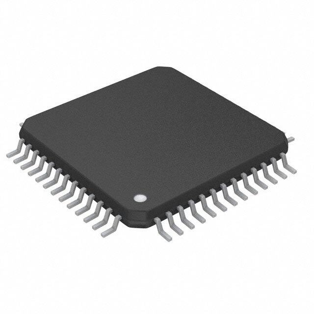
MSP430F479,MSP430F478,MSP430F477 SLAS629B–MARCH2009–REVISEDMAY2020 www.ti.com 4 Terminal Configuration and Functions 4.1 Pin Diagrams Figure4-1showsthepinoutforthe80-pinPNpackage. Figure4-1.80-PinPNPackage(TopView) 6 TerminalConfigurationandFunctions Copyright©2009–2020,TexasInstrumentsIncorporated SubmitDocumentationFeedback ProductFolderLinks:MSP430F479 MSP430F478 MSP430F477
MSP430F479,MSP430F478,MSP430F477 www.ti.com SLAS629B–MARCH2009–REVISEDMAY2020 Figure4-2showsthepinoutforthe113-pinZCAandZQWpackages.Forpinassignments,seeTable4-1. NOTE:Fortheterminalassignments,seeSection4.2. Figure4-2.113-PinZCAandZQWPackages(TopView) Copyright©2009–2020,TexasInstrumentsIncorporated TerminalConfigurationandFunctions 7 SubmitDocumentationFeedback ProductFolderLinks:MSP430F479 MSP430F478 MSP430F477
MSP430F479,MSP430F478,MSP430F477 SLAS629B–MARCH2009–REVISEDMAY2020 www.ti.com 4.2 Signal Descriptions Table4-1describesthedevicesignals. Table4-1.SignalDescriptions PINNO. SIGNALNAME ZCA, I/O DESCRIPTION PN ZQW AVCC 52 F12 Analogsupplyvoltage,positiveterminal. AVSS 53 E12 Analogsupplyvoltage,negativeterminal. DVCC1 1 A1 Digitalsupplyvoltage,positiveterminal.Suppliesalldigitalparts. DVSS1 79 A3 Digitalsupplyvoltage,negativeterminal.Suppliesalldigitalparts. DVCC2 80 A2 Digitalsupplyvoltage,positiveterminal.Suppliesalldigitalparts. DVSS2 78 B2,B3 Digitalsupplyvoltage,negativeterminal.Suppliesalldigitalparts. General-purposedigitalI/Opin P1.0/TA0 58 C11 I/O Timer_A,capture:CCI0Ainput,compare:Out0output BSLtransmit General-purposedigitalI/Opin Timer_A,capture:CCI0Binput,compare:Out0output P1.1/TA0/MCLK 57 C12 I/O MCLKsignaloutput BSLreceive General-purposedigitalI/Opin P1.2/TA1/A4- 56 D11 I/O Timer_A,capture:CCI1Ainput,compare:Out1output SD16negativeanaloginputA4 General-purposedigitalI/Opin Timer_A,capture:CCI2Ainput,compare:Out2output P1.3/TBOUTH/SVSOUT/A4 SetallPWMdigitaloutputportstohighimpedance-Timer_BTB0to 55 D12 I/O + TB2 SVScomparatoroutput SD16positiveanaloginputA4 General-purposedigitalI/Opin Timer_B,clocksignalTBCLKinput P1.4/TBCLK/SMCLK/A3- 54 E11 I/O SMCLKsignaloutput SD16negativeanaloginputA3 General-purposedigitalI/Opin Timer_A,clocksignalTACLKinput P1.5/TACLK/ACLK/A3+ 51 F11 I/O ACLKsignaloutput SD16positiveanaloginputA3 General-purposedigitalI/Opin Comparator_Ainput0 P1.6/CA0/A2-/DAC0 50 G12 I/O SD16negativeanaloginputA2 DAC12.0output General-purposedigitalI/Opin P1.7/CA1/A2+ 49 G11 I/O Comparator_Ainput1 SD16positiveanaloginputA2 General-purposedigitalI/Opin P2.0/TA2/S1 4 C2,C3 I/O Timer_A,capture:CCI2A/Binput,compare:Out2output LCDsegmentoutput1 General-purposedigitalI/Opin P2.1/TB0/S0 3 C1 I/O Timer_B,capture:CCI0A/Binput,compare:Out0output LCDsegmentoutput0 8 TerminalConfigurationandFunctions Copyright©2009–2020,TexasInstrumentsIncorporated SubmitDocumentationFeedback ProductFolderLinks:MSP430F479 MSP430F478 MSP430F477
MSP430F479,MSP430F478,MSP430F477 www.ti.com SLAS629B–MARCH2009–REVISEDMAY2020 Table4-1.SignalDescriptions(continued) PINNO. SIGNALNAME ZCA, I/O DESCRIPTION PN ZQW General-purposedigitalI/Opin P2.2/TB1 2 B1 I/O Timer_B,capture:CCI1A/Binput,compare:Out1output General-purposedigitalI/Opin P2.3/TB2 77 B4 I/O Timer_B,capture:CCI2A/Binput,compare:Out2output General-purposedigitalI/Opin P2.4/UCA0TXD/ UCA0SIMO 76 A4 I/O USCIAtransmitdataoutputinUARTmode,slavedatain/masteroutin SPImode General-purposedigitalI/Opin P2.5/UCA0RXD/ UCA0SOMI 75 D4 I/O USCIA0receivedatainputinUARTmode,slavedataout/masterinin SPImode General-purposedigitalI/Opin P2.6/CAOUT/S2 5 D1 I/O Comparator_Aoutput LCDsegmentoutput2 General-purposedigitalI/Opin P2.7/S3 6 D2 I/O LCDsegmentoutput3 General-purposedigitalI/Opin P3.0/UCB0STE/UCA0CLK 41 M12 I/O USCIB0slavetransmitenable USCIA0clockinput/output General-purposedigitalI/Opin P3.1/UCB0SIMO/ 42 L12 I/O USCIB0slavein/masteroutinSPImode,SDAI2CdatainI2Cmode UCB0SDA/S26 LCDsegmentoutput26 General-purposedigitalI/Opin P3.2/UCB0SOMI/ 43 K11 I/O USCIB0slaveout/masterininSPImode,SCLI2CclockinI2Cmode UCB0SCL/S27 LCDsegmentoutput27 General-purposedigitalI/O P3.3/UCB0CLK/UCA0STE 44 K12 I/O USCIB0clockinput/output,USCIA0slavetransmitenable General-purposedigitalI/Opin P3.4/S28 45 J11 I/O LCDsegmentoutput28 General-purposedigitalI/Opin P3.5/S29 46 J12 I/O LCDsegmentoutput29 General-purposedigitalI/Opin P3.6/S30 47 H11 I/O LCDsegmentoutput30 General-purposedigitalI/Opin P3.7/S31 48 H12 I/O LCDsegmentoutput31 General-purposedigitalI/Opin P4.0/S11 18 K2 I/O LCDsegmentoutput11 General-purposedigitalI/Opin P4.1/S10 17 K1 I/O LCDsegmentoutput10 General-purposedigitalI/Opin P4.2/S9 16 J2 I/O LCDsegmentoutput9 General-purposedigitalI/Opin P4.3/S8 15 J1 I/O LCDsegmentoutput8 General-purposedigitalI/Opin P4.4/S7 14 H2 I/O LCDsegmentoutput7 General-purposedigitalI/Opin P4.5/S6 13 H1 I/O LCDsegmentoutput6 Copyright©2009–2020,TexasInstrumentsIncorporated TerminalConfigurationandFunctions 9 SubmitDocumentationFeedback ProductFolderLinks:MSP430F479 MSP430F478 MSP430F477
MSP430F479,MSP430F478,MSP430F477 SLAS629B–MARCH2009–REVISEDMAY2020 www.ti.com Table4-1.SignalDescriptions(continued) PINNO. SIGNALNAME ZCA, I/O DESCRIPTION PN ZQW General-purposedigitalI/Opin P4.6/S5 12 G2 I/O LCDsegmentoutput5 General-purposedigitalI/Opin P4.7/S4 11 G1 I/O LCDsegmentoutput4 COM0 33 L8 O Commonoutput,COM0-3areusedforLCDbackplanes General-purposedigitalI/Opin P5.0/S20 27 L5 I/O LCDsegmentoutput20 General-purposedigitalI/Opin P5.1/S21 28 M5 I/O LCDsegmentoutput21 General-purposedigitalI/Opin P5.2/COM1 34 M8 I/O commonoutput,COM0-3areusedforLCDbackplanes General-purposedigitalI/Opin P5.3/COM2 35 L9 I/O commonoutput,COM0-3areusedforLCDbackplanes General-purposedigitalI/Opin P5.4/COM3 36 M9 I/O commonoutput,COM0-3areusedforLCDbackplanes CapacitorconnectionforLCDchargepump LCDCAP/R33 37 J9 I/O inputportofmostpositiveanalogLCDlevel(V4) General-purposedigitalI/Opin P5.5/R23 38 M10 I/O inputportofthesecondmostpositiveanalogLCDlevel(V3) General-purposedigitalI/Opin P5.6/LCDREF/R13 39 L10 I/O ExternalLCDreferencevoltageinput inputportofthethirdmostpositiveanalogLCDlevel(V3orV2) General-purposedigitalI/Opin P5.7/R03 40 M11 I/O inputportofthefourthmostpositiveanalogLCDlevel(V1) General-purposedigitalI/Opin P6.0/A0+ 67 B8 I/O SD16positiveanaloginputA0 General-purposedigitalI/Opin P6.1/A0- 66 B9 I/O SD16positivenegativeinputA0 P6.2 65 A9 I/O General-purposedigitalI/Opin General-purposedigitalI/Opin P6.3/A1+ 64 D9 I/O SD16positiveanaloginputA1 General-purposedigitalI/Opin P6.4/A1- 63 A10 I/O SD16positivenegativeinputA1 P6.5 62 B10 I/O General-purposedigitalI/Opin P6.6 61 A11 I/O General-purposedigitalI/Opin General-purposedigitalI/Opin P6.7/SVSIN 59 B12 I/O SVSinput S12 19 L1 O LCDsegmentoutput12 S13 20 M1 O LCDsegmentoutput13 S14 21 M2 O LCDsegmentoutput14 S15 22 M3 O LCDsegmentoutput15 S16 23 L3 O LCDsegmentoutput16 S17 24 L4 O LCDsegmentoutput17 S18 25 M4 O LCDsegmentoutput18 S19 26 J4 O LCDsegmentoutput19 S22 29 L6 O LCDsegmentoutput22 10 TerminalConfigurationandFunctions Copyright©2009–2020,TexasInstrumentsIncorporated SubmitDocumentationFeedback ProductFolderLinks:MSP430F479 MSP430F478 MSP430F477
MSP430F479,MSP430F478,MSP430F477 www.ti.com SLAS629B–MARCH2009–REVISEDMAY2020 Table4-1.SignalDescriptions(continued) PINNO. SIGNALNAME ZCA, I/O DESCRIPTION PN ZQW S23 30 M6 O LCDsegmentoutput23 S24 31 L7 O LCDsegmentoutput24 S25 32 M7 O LCDsegmentoutput25 GND 7 E2 Ground.Itisusedtoshieldtheoscillator.SeeNote1. InputportforcrystaloscillatorXT1.Standardorwatchcrystalscanbe XIN 8 E1 I connected. OutputportforcrystaloscillatorXT1.Standardorwatchcrystalscanbe XOUT 9 F1 O connected. GND 10 F2 Ground.Itisusedtoshieldtheoscillator.(1) V 60 A12 O Inputforanexternalreferencevoltage/internalreferencevoltageoutput REF Resetinput,nonmaskableinterruptinputport,orbootloaderstart(in RST/NMI 74 B5 I flashdevices). Testclock(JTAG).TCKistheclockinputportfordeviceprogramming TCK 73 A5 I testandbootloaderstart. Testdatainputortestclockinput.Thedeviceprotectionfuseis TDI/TCLK 71 A6 I connectedtoTDI/TCLK. Testdataoutputport.TDO/TDIdataoutputorprogrammingdatainput TDO/TDI 70 B7 I/O terminal. Testmodeselect.TMSisusedasaninputportfordeviceprogramming TMS 72 B6 I andtest. XT2OUT 68 A8 O OutputterminalofcrystaloscillatorXT2 XT2IN 69 A7 I InputportforcrystaloscillatorXT2 B11,D6, D7,D8, E4,E5, E6,E7, E8,E9, F4,F5, F8,F9, Reserved NA G4, UnusedBGAballs.ConnectiontoDVSS/AVSSrecommended. G5,G8, G9,H4, H5,H6, H7,H8, H9,J5,J6, J7,J8,L2, L11 (1) ItisrecommendedtoconnectGNDexternallytoDV . SS Copyright©2009–2020,TexasInstrumentsIncorporated TerminalConfigurationandFunctions 11 SubmitDocumentationFeedback ProductFolderLinks:MSP430F479 MSP430F478 MSP430F477
MSP430F479,MSP430F478,MSP430F477 SLAS629B–MARCH2009–REVISEDMAY2020 www.ti.com 5 Specifications 5.1 Absolute Maximum Ratings overoperatingfree-airtemperaturerange(unlessotherwisenoted)(1) MIN MAX UNIT VoltageappliedatV toV –0.3 4.1 V CC SS Voltageappliedtoanypin(2) –0.3 V +0.3 V CC Diodecurrentatanydeviceterminal ±2 mA Unprogrammeddevice –55 150 Storagetemperature,T (3) °C stg Programmeddevice –40 85 (1) StressesbeyondthoselistedunderAbsoluteMaximumRatingsmaycausepermanentdamagetothedevice.Thesearestressratings only,andfunctionaloperationofthedeviceattheseoranyotherconditionsbeyondthoseindicatedunderRecommendedOperating Conditionsisnotimplied.Exposuretoabsolute-maximum-ratedconditionsforextendedperiodsmayaffectdevicereliability. (2) AllvoltagesarereferencedtoV .TheJTAGfuse-blowvoltage,V ,isallowedtoexceedtheabsolutemaximumrating.Thevoltageis SS FB appliedtotheTDI/TCLKpinwhenblowingtheJTAGfuse. (3) HighertemperaturemaybeappliedduringboardsolderingprocessaccordingtothecurrentJEDECJ-STD-020specificationwithpeak reflowtemperaturesnothigherthanclassifiedonthedevicelabelontheshippingboxesorreels. 5.2 ESD Ratings VALUE UNIT Human-bodymodel(HBM),perANSI/ESDA/JEDECJS-001(1) ±1000 V Electrostaticdischarge V (ESD) Charged-devicemodel(CDM),perJEDECspecificationJESD22-C101(2) ±250 (1) JEDECdocumentJEP155statesthat500-VHBMallowssafemanufacturingwithastandardESDcontrolprocess.Pinslistedas ±1000Vmayactuallyhavehigherperformance. (2) JEDECdocumentJEP157statesthat250-VCDMallowssafemanufacturingwithastandardESDcontrolprocess.Pinslistedas±250V mayactuallyhavehigherperformance. 12 Specifications Copyright©2009–2020,TexasInstrumentsIncorporated SubmitDocumentationFeedback ProductFolderLinks:MSP430F479 MSP430F478 MSP430F477
MSP430F479,MSP430F478,MSP430F477 www.ti.com SLAS629B–MARCH2009–REVISEDMAY2020 5.3 Recommended Operating Conditions TypicalvaluesarespecifiedatV =3.3VandT =25°C(unlessotherwisenoted) CC A MIN NOM MAX UNIT Duringprogramexecution(AV =DV =DV =V ) 1.8 3.6 CC CC1 CC2 CC VCC Supplyvoltage Duringflashmemoryprogramming(AVCC=DVCC1=DVCC2= 2.7 3.6 V V ) CC V Supplyground(AV =DV =DV =V ) 0 0 V SS SS SS1 SS2 SS T Operatingfree-airtemperaturerange –40 85 °C A LFselected,XTS_FLL=0 Watchcrystal 32.768 kHz LFXT1crystal f(LFXT1) frequency(1) XT1selected,XTS_FLL=1 Ceramicresonator 0.45 6 MHz XT1selected,XTS_FLL=1 Crystal 1 6 Ceramicresonator 0.45 8 f XT2crystalfrequency MHz (XT2) Crystal 1 8 V =1.8V DC 4.15 CC f Processorfrequency(MCLK,SMCLK,ACLK) MHz (System) V =2.5V DC 8 CC (1) InLFmode,theLFXT1oscillatorrequiresawatchcrystal.InXT1mode,LFXT1acceptsaceramicresonatororacrystal. Supply voltage range Supply voltage range during program during flash memory programming execution Figure5-1.FrequencyvsSupplyVoltage Copyright©2009–2020,TexasInstrumentsIncorporated Specifications 13 SubmitDocumentationFeedback ProductFolderLinks:MSP430F479 MSP430F478 MSP430F477
MSP430F479,MSP430F478,MSP430F477 SLAS629B–MARCH2009–REVISEDMAY2020 www.ti.com 5.4 Supply Current Into AV and DV Excluding External Current CC CC overrecommendedrangesofsupplyvoltageandoperatingfree-airtemperature(unlessotherwisenoted) PARAMETER TESTCONDITION MIN TYP MAX UNIT Activemode(1) V =2.2V 262 295 CC f =f =1MHz, I (MCLK) (SMCLK) T =–40°Cto85°C µA (AM) f(ACLK)=32768Hz, A VCC=3V 420 460 XTS=0,SELM=0or1 V =2.2V 32 62 I Lowpowermode(LPM0)(1) T =–40°Cto85°C CC µA (LPM0) A V =3V 51 77 CC Low-powermode(LPM2), V =2.2V 5 9 CC I f =f =0MHz, T =–40°Cto85°C µA (LPM2) (MCLK) (SMCLK) A f(ACLK)=32768Hz,SCG0=0(2) VCC=3V 7 13 T =–40°C 1.0 1.8 A T =25°C 1.0 1.8 A V =2.2V Low-powermode(LPM3), T =60°C CC 1.1 2.0 A f =f =0MHz, (MCLK) (SMCLK) I f(ACLK)=32768Hz,SCG0=1, TA=85°C 2.3 4.0 µA (LPM3) BasicTimer1enabled,ACLKselected, T =–40°C 1.2 2.0 A LCD_Aenabled,LCDCPEN=0, (staticmode,fLCD=f(ACLK)/32)(2) (3) TA=25°C V =3V 1.2 2.0 CC T =60°C 1.4 2.2 A T =85°C 2.7 4.5 A T =–40°C 1.0 3.0 A Low-powermode(LPM3), T =25°C V =2.2V 1.1 3.2 A CC f =f =0MHz, (MCLK) (SMCLK) I f(ACLK)=32768Hz,SCG0=1, TA=85°C 3.5 6.0 µA (LPM3) BasicTimer1enabled,ACLKselected, T =–40°C 1.8 3.3 A LCD_Aenabled,LCDCPEN=0, (4-muxmode;fLCD=f(ACLK)/32)(2) (3) TA=25°C VCC=3V 2.0 4.0 T =85°C 4.2 7.5 A T =–40°C 0.1 0.5 A T =25°C 0.1 0.5 A V =2.2V CC T =60°C 0.7 1.1 A Low-powermode(LPM4), T =85°C 1.7 3.0 A I f =0MHz,f =0MHz, µA (LPM4) (MCLK) (SMCLK) f(ACLK)=0Hz,SCG0=1(2) TA=–40°C 0.1 0.8 T =25°C 0.1 0.8 A V =3V CC T =60°C 0.8 1.2 A T =85°C 1.5 3.5 A (1) Timer_Aisclockedbyf =1MHz.Allinputsaretiedto0VortoV .Outputsdonotsourceorsinkanycurrent. (DCOCLK) CC (2) Allinputsaretiedto0VortoV .Outputsdonotsourceorsinkanycurrent. CC (3) TheLPM3currentsarecharacterizedwithaMicroCrystalCC4V-T1A(9pF)crystalandOSCCAPx=1h. Currentconsumptionofactivemodeversussystemfrequency: I =I ×f [MHz] (AM) (AM)[1MHz] (System) Currentconsumptionofactivemodeversussupplyvoltage: I =I +200µA/V×(V –2.2V) (AM) (AM)[3V] CC 14 Specifications Copyright©2009–2020,TexasInstrumentsIncorporated SubmitDocumentationFeedback ProductFolderLinks:MSP430F479 MSP430F478 MSP430F477
MSP430F479,MSP430F478,MSP430F477 www.ti.com SLAS629B–MARCH2009–REVISEDMAY2020 Figure5-2.I --LPM4CurrentvsTemperature LPM4 5.5 Schmitt-Trigger Inputs – Ports P1 to P6, RST/NMI, JTAG (TCK, TMS, TDI/TCLK,TDO/TDI) overrecommendedrangesofsupplyvoltageandoperatingfree-airtemperature(unlessotherwisenoted) PARAMETER TESTCONDITIONS MIN MAX UNIT V =2.2V 1.1 1.55 CC V Positive-goinginputthresholdvoltage V IT+ V =3V 1.5 1.98 CC V =2.2V 0.4 0.9 CC V Negative-goinginputthresholdvoltage V IT– V =3V 0.9 1.3 CC V =2.2V 0.3 1.1 CC V Inputvoltagehysteresis(V –V ) V hys IT+ IT– V =3V 0.5 1 CC 5.6 Inputs Px.y, TAx overrecommendedrangesofsupplyvoltageandoperatingfree-airtemperature(unlessotherwisenoted) PARAMETER TESTCONDITIONS V MIN MAX UNIT CC PortP1,P2:P1.xtoP2.x,externaltriggersignal 2.2V 62 t(int) Externalinterrupttiming fortheinterruptflag(1) 3V 50 ns 2.2V 62 t Timer_Acapturetiming TA0,TA1,TA2 ns (cap) 3V 50 f(TAext) Timer_Aclockfrequencyexternally 2.2V 8 TACLK,INCLKt =t MHz f appliedtopin (H) (L) 3V 10 (TBext) f 2.2V 8 (TAint) TimerAclockfrequency SMCLKorACLKsignalselected MHz f 3V 10 (TBint) (1) Theexternalsignalsetstheinterruptflageverytimetheminimumt parametersaremet.Itmaybesetevenwithtriggersignals (int) shorterthant . (int) 5.7 Leakage Current – Ports P1 to P6 overrecommendedrangesofsupplyvoltageandoperatingfree-airtemperature(unlessotherwisenoted)(1) PARAMETER TESTCONDITIONS MIN MAX UNIT I Leakagecurrent,PortPx V (2) V =2.2V,3V ±50 nA lkg(Px.y) (Px.y) CC (1) TheleakagecurrentismeasuredwithV orV appliedtothecorrespondingpins,unlessotherwisenoted. SS CC (2) Theportpinmustbeselectedasinput. Copyright©2009–2020,TexasInstrumentsIncorporated Specifications 15 SubmitDocumentationFeedback ProductFolderLinks:MSP430F479 MSP430F478 MSP430F477
MSP430F479,MSP430F478,MSP430F477 SLAS629B–MARCH2009–REVISEDMAY2020 www.ti.com 5.8 Outputs – Ports P1 to P6 overrecommendedrangesofsupplyvoltageandoperatingfree-airtemperature(unlessotherwisenoted) PARAMETER TESTCONDITIONS MIN MAX UNIT I =–1.5mA,V =2.2V(1) V –0.25 V OH(max) CC CC CC I =–6mA,V =2.2V(2) V –0.6 V OH(max) CC CC CC V High-leveloutputvoltage V OH I =–1.5mA,V =3V(1) V –0.25 V OH(max) CC CC CC I =–6mA,V =3V(2) V –0.6 V OH(max) CC CC CC I =1.5mA,V =2.2V(1) V V +0.25 OL(max) CC SS SS I =6mA,V =2.2V(2) V V +0.6 OL(max) CC SS SS V Low-leveloutputvoltage V OL I =1.5mA,V =3V(1) V V +0.25 OL(max) CC SS SS I =6mA,V =3V(2) V V +0.6 OL(max) CC SS SS (1) Themaximumtotalcurrent,I andI ,foralloutputscombined,shouldnotexceed±12mAtosatisfythemaximumspecified OH(max) OL(max) voltagedrop. (2) Themaximumtotalcurrent,I andI ,foralloutputscombined,shouldnotexceed±48mAtosatisfythemaximumspecified OH(max) OL(max) voltagedrop. 5.9 Output Frequency overrecommendedrangesofsupplyvoltageandoperatingfree-airtemperature(unlessotherwisenoted) PARAMETER TESTCONDITIONS MIN TYP MAX UNIT f 1≤×≤6,0≤y≤7 C =20F,I =±1.5mA V =2.2V,3V DC f MHz (Px.y) L L CC System f P1.1/TA0/MCLK C =20pF f MHz (MCLK) L System f =f 40% 60% (MCLK) (XT1) Dutycycleofoutput P1.1/TA0/MCLK, t(Xdc) frequency CL=20pF,VCC=2.2V,3V f(MCLK)=f(DCOCLK) 5105%n–s 50% 5105%n+s 16 Specifications Copyright©2009–2020,TexasInstrumentsIncorporated SubmitDocumentationFeedback ProductFolderLinks:MSP430F479 MSP430F478 MSP430F477
MSP430F479,MSP430F478,MSP430F477 www.ti.com SLAS629B–MARCH2009–REVISEDMAY2020 5.10 Typical Characteristics – Outputs overrecommendedrangesofsupplyvoltageandoperatingfree-airtemperature(unlessotherwisenoted) Figure5-3.TypicalLow-LevelOutputCurrentvsTypicalLow- Figure5-4.TypicalLow-LevelOutputCurrentvsTypicalLow- LevelOutputCurrent LevelOutputCurrent Figure5-5.TypicalHigh-LevelOutputCurrentvsTypicalHigh- Figure5-6.TypicalHigh-LevelOutputCurrentvsTypicalHigh- LevelOutputCurrent LevelOutputCurrent Copyright©2009–2020,TexasInstrumentsIncorporated Specifications 17 SubmitDocumentationFeedback ProductFolderLinks:MSP430F479 MSP430F478 MSP430F477
MSP430F479,MSP430F478,MSP430F477 SLAS629B–MARCH2009–REVISEDMAY2020 www.ti.com 5.11 Wake-up Timing From LPM3 overrecommendedrangesofsupplyvoltageandoperatingfree-airtemperature(unlessotherwisenoted) PARAMETER TESTCONDITIONS MIN MAX UNIT f=1MHz 6 t Delaytime f=2MHz V =2.2V,3V 6 µs d(LPM3) CC f=3MHz 6 5.12 POR – Brownout Reset (BOR) overrecommendedrangesofsupplyvoltageandoperatingfree-airtemperature(unlessotherwisenoted)(1) PARAMETER TESTCONDITIONS MIN TYP MAX UNIT t 2000 µs d(BOR) 0.7× V dV /dt≤3V/s(seeFigure5-7) V CC(start) CC V (B_IT–) V Brownout(2) dV /dt≤3V/s(seeFigure5-7throughFigure5-9) 1.71 V (B_IT–) CC V dV /dt≤3V/s(seeFigure5-7) mV hys(B_IT–) CC PulsedurationneededatRST/NMIpintoaccepted t 2 µs (reset) resetinternally,V =2.2V,3V CC (1) ThecurrentconsumptionofthebrownoutmoduleisalreadyincludedintheI currentconsumptiondata.ThevoltagelevelV + CC (B_IT–) V ≤1.89V. hys(B_IT–) (2) Duringpowerup,theCPUbeginscodeexecutionfollowingaperiodoft afterV =V +V .ThedefaultFLL+settings d(BOR) CC (B_IT–) hys(B_IT–) mustnotbechangeduntilV ≥V ,whereV istheminimumsupplyvoltageforthedesiredoperatingfrequency.Seethe CC CC(min) CC(min) MSP430x4xxFamilyUser’sGuide(SLAU056)formoreinformationonthebrownoutandSVScircuit. V CC V hys(B_IT-) V (B_IT-) V CC(start) 1 0 t d(BOR) Figure5-7.POR,BORvsSupplyVoltage 18 Specifications Copyright©2009–2020,TexasInstrumentsIncorporated SubmitDocumentationFeedback ProductFolderLinks:MSP430F479 MSP430F478 MSP430F477
MSP430F479,MSP430F478,MSP430F477 www.ti.com SLAS629B–MARCH2009–REVISEDMAY2020 2 VCC tpw 3 V V = 3 V CC Typical Conditions 1.5 V - op) 1 dr C( VC VCC(drop) 0.5 0 0.001 1 1000 1 ns 1 ns t - Pulse Width -ms t - Pulse Width -ms pw pw Figure5-8.V LevelwithaSquareVoltageDroptoGenerateaPORorBORSignal CC(drop) VCC tpw 2 3 V V = 3 V CC 1.5 Typical Conditions V -p) o 1 r d C( VCC(drop) C V 0.5 t = t f r 0 0.001 1 1000 t t f r tpw - Pulse Width -ms tpw - Pulse Width -ms Figure5-9.V LevelWithaTriangleVoltageDroptoGenerateaPORorBORSignal CC(drop) Copyright©2009–2020,TexasInstrumentsIncorporated Specifications 19 SubmitDocumentationFeedback ProductFolderLinks:MSP430F479 MSP430F478 MSP430F477
MSP430F479,MSP430F478,MSP430F477 SLAS629B–MARCH2009–REVISEDMAY2020 www.ti.com 5.13 SVS (Supply Voltage Supervisor and Monitor) overrecommendedrangesofsupplyvoltageandoperatingfree-airtemperature(unlessotherwisenoted) PARAMETER TESTCONDITIONS MIN TYP MAX UNIT dV /dt>30V/ms(seeFigure5-10) 5 150 CC t µs (SVSR) dV /dt≤30V/ms 2000 CC t SVSon,switchfromVLD=0toVLD≠0,V =3V 20 150 µs d(SVSon) CC t VLD≠0(1) 12 µs settle V VLD≠0,V /dt≤3V/s(seeFigure5-10) 1.55 1.7 V (SVSstart) CC VLD=1 70 120 210 mV VCC/dt≤3V/s(seeFigure5-10) VLD=2to14 V(SVS_IT–) V(SVS_IT–) V ×0.001 ×0.016 hys(SVS_IT–) V /dt≤3V/s(seeFigure5-10),externalvoltage CC VLD=15 4.4 20 mV appliedonA7 VLD=1 1.8 1.9 2.05 VLD=2 1.94 2.1 2.23 VLD=3 2.05 2.2 2.37 VLD=4 2.14 2.3 2.48 VLD=5 2.24 2.4 2.6 VLD=6 2.33 2.5 2.71 VLD=7 2.46 2.65 2.86 V /dt≤3V/s(seeFigure5-10) CC VLD=8 2.58 2.8 3 V V (SVS_IT–) VLD=9 2.69 2.9 3.13 VLD=10 2.83 3.05 3.29 VLD=11 2.94 3.2 3.42 VLD=12 3.11 3.35 3.61(2) VLD=13 3.24 3.5 3.76(2) VLD=14 3.43 3.7(2) 3.99(2) V /dt≤3V/s(seeFigure5-10),externalvoltage CC VLD=15 1.1 1.2 1.3 appliedonA7 I (3) VLD≠0,V =2.2V,3V 10 15 µA CC(SVS) CC (1) t isthesettlingtimethatthecomparatoroutputneedstohaveastablelevelafterVLDisswitchedfromVLD≠0toadifferentVLD settle valuefrom2to15.Theoverdriveisassumedtobe>50mV. (2) Therecommendedoperatingvoltagerangeislimitedto3.6V. (3) ThecurrentconsumptionoftheSVSmoduleisnotincludedintheI currentconsumptiondata. CC 20 Specifications Copyright©2009–2020,TexasInstrumentsIncorporated SubmitDocumentationFeedback ProductFolderLinks:MSP430F479 MSP430F478 MSP430F477
MSP430F479,MSP430F478,MSP430F477 www.ti.com SLAS629B–MARCH2009–REVISEDMAY2020 Software Sets VLD>0: VCC SVS isActive Vhys(SVS_IT-) V (SVS_IT-) V (SVSstart) Vhys(B_IT-) V(B_IT-) VCC(start) Brown Brownout Out Region Brownout Region 1 0 SVSOut td(BOR) td(BOR) SVS Circuit isActive From VLD > to VCC < V(B_IT-) 1 0 td(SVSon) td(SVSR) Set POR 1 undefined 0 Figure5-10.SVSReset(SVSR)vsSupplyVoltage V CC t pw 3 V 2 Rectangular Drop V CC(drop) 1.5 Triangular Drop V -p) ro 1 d ( C 1 ns 1 ns C V 0.5 V CC t pw 3 V 0 1 10 100 1000 tpw - Pulse Width -ms V CC(drop) t = t f r t t f r t - Pulse Width -ms Figure5-11.V withaSquareVoltageDropandaTriangleVoltageDroptoGenerateanSVSSignal CC(drop) Copyright©2009–2020,TexasInstrumentsIncorporated Specifications 21 SubmitDocumentationFeedback ProductFolderLinks:MSP430F479 MSP430F478 MSP430F477
MSP430F479,MSP430F478,MSP430F477 SLAS629B–MARCH2009–REVISEDMAY2020 www.ti.com 5.14 DCO overrecommendedrangesofsupplyvoltageandoperatingfree-airtemperature(unlessotherwisenoted) PARAMETER TESTCONDITIONS V MIN TYP MAX UNIT CC N =01Eh,FN_8=FN_4=FN_3=FN_2=0,D=2, f (DCO) 2.2V,3V 1 MHz (DCOCLK) DCOPLUS=0 2.2V 0.3 0.65 1.25 f FN_8=FN_4=FN_3=FN_2=0,DCOPLUS=1 MHz (DCO=2) 3V 0.3 0.7 1.3 2.2V 2.5 5.6 10.5 f FN_8=FN_4=FN_3=FN_2=0,DCOPLUS=1(1) MHz (DCO=27) 3V 2.7 6.1 11.3 2.2V 0.7 1.3 2.3 f FN_8=FN_4=FN_3=FN_2=1,DCOPLUS=1 MHz (DCO=2) 3V 0.8 1.5 2.5 2.2V 5.7 10.8 18 f FN_8=FN_4=FN_3=FN_2=1,DCOPLUS=1(1) MHz (DCO=27) 3V 6.5 12.1 20 2.2V 1.2 2 3 f FN_8=FN_4=0,FN_3=1,FN_2=x,DCOPLUS=1 MHz (DCO=2) 3V 1.3 2.2 3.5 2.2V 9 15.5 25 f FN_8=FN_4=0,FN_3=1,FN_2=x,DCOPLUS=1(1) MHz (DCO=27) 3V 10.3 17.9 28.5 2.2V 1.8 2.8 4.2 f FN_8=0,FN_4=1,FN_3=FN_2=x,DCOPLUS=1 MHz (DCO=2) 3V 2.1 3.4 5.2 2.2V 13.5 21.5 33 f FN_8=0,FN_4=1,FN_3=FN_2=x,DCOPLUS=1(1) MHz (DCO=27) 3V 16 26.6 41 2.2V 2.8 4.2 6.2 f FN_8=1,FN_4=1=FN_3=FN_2=x,DCOPLUS=1 MHz (DCO=2) 3V 4.2 6.3 9.2 2.2V 21 32 46 f FN_8=1,FN_4=1=FN_3=FN_2=x,DCOPLUS=1(1) MHz (DCO=27) 3V 30 46 70 StepsizebetweenadjacentDCOtaps: 1<TAP≤20 1.06 1.11 S n Sn=fDCO(Tapn+1)/fDCO(Tapn)(seeFigure5-13fortaps21to27) TAP=27 1.07 1.17 Temperaturedrift,N =01Eh, 2.2V –0.2 –0.3 –0.4 Dt FN_8=FN_4=FN_(3DC=OF)N_2=0,D=2,DCOPLUS=0(2) 3V –0.2 –0.3 –0.4 %/°C DriftwithV variation,N =01Eh, DV FN_8=FNC_C4=FN_3=F(NDC_O2)=0,D=2,DCOPLUS=0(2) 0 5 15 %/V (1) Donotexceedthemaximumsystemfrequency. (2) Thisparameterisnotproductiontested. f f (DCO) (DCO) f(DCO3V) f(DCO20°C) 1.0 1.0 0 1.8 2.4 3.0 3.6 -40 -20 0 20 40 60 85 V - V T - °C CC A Figure5-12.DCOFrequencyvsSupplyVoltageV andvsAmbientTemperature CC 22 Specifications Copyright©2009–2020,TexasInstrumentsIncorporated SubmitDocumentationFeedback ProductFolderLinks:MSP430F479 MSP430F478 MSP430F477
MSP430F479,MSP430F478,MSP430F477 www.ti.com SLAS629B–MARCH2009–REVISEDMAY2020 s p a T 1.17 O C D n e e w et b o Rati 1.11 Max e z si p e t S n- 1.07 S 1.06 Min 1 20 27 DCO Tap Figure5-13.DCOTapStepSize Legend Tolerance at Tap 27 O) C D f( DCO Frequency Adjusted by Bits 9 5 2 to 2 in SCFI1 {N } {DCO} Tolerance at Tap 2 Overlapping DCO Ranges: Uninterrupted Frequency Range FN_2=0 FN_2=1 FN_2=x FN_2=x FN_2=x FN_3=0 FN_3=0 FN_3=1 FN_3=x FN_3=x FN_4=0 FN_4=0 FN_4=0 FN_4=1 FN_4=x FN_8=0 FN_8=0 FN_8=0 FN_8=0 FN_8=1 Figure5-14.FiveOverlappingDCORangesControlledbyFN_xBits Copyright©2009–2020,TexasInstrumentsIncorporated Specifications 23 SubmitDocumentationFeedback ProductFolderLinks:MSP430F479 MSP430F478 MSP430F477
MSP430F479,MSP430F478,MSP430F477 SLAS629B–MARCH2009–REVISEDMAY2020 www.ti.com 5.15 Crystal Oscillator, LFXT1, Low-Frequency Mode overrecommendedrangesofsupplyvoltageandoperatingfree-airtemperature(unlessotherwisenoted) (1) PARAMETER TESTCONDITIONS V MIN TYP MAX UNIT CC LFXT1oscillatorcrystal 1.8Vto f XTS=0,LFXT1Sx=0or1 32768 Hz LFXT1,LF frequency,LFmode0,1 3.6V XTS=0,LFXT1Sx=0, 500 OscillationallowanceforLF fLFXT1,LF=32768kHz,CL,eff=6pF OA kΩ LF crystals XTS=0,LFXT1Sx=0, 200 f =32768kHz,C =12pF LFXT1,LF L,eff XTS=0,XCAPx=0 1 Integratedeffectiveload XTS=0,XCAPx=1 5.5 CL,eff capacitance,LFmode(2) XTS=0,XCAPx=2 8.5 pF XTS=0,XCAPx=3 11 XTS=0,MeasuredatP1.5/ACLK, Dutycycle,LFmode 2.2V,3V 30 50 70 % f =32768Hz LFXT1,LF Oscillatorfaultfrequency,LF XTS=0,XCAPx=0,LFXT1Sx= fFault,LF mode(3) 3(4) 2.2V,3V 10 10000 Hz (1) ToimproveEMIonthelow-powerLFXT1oscillator,particularlyintheLFmode(32kHz),thefollowingguidelinesshouldbeobserved. • KeepthetracebetweentheMCUandthecrystalasshortaspossible. • Designagoodgroundplanearoundtheoscillatorpins. • PreventcrosstalkfromotherclockordatalinesintooscillatorpinsXINandXOUT. • AvoidrunningPCBtracesunderneathoradjacenttotheXINandXOUTpins. • UseassemblymaterialsandprocessesthatavoidanyparasiticloadontheoscillatorXINandXOUTpins. • Ifconformalcoatingisused,ensurethatitdoesnotinducecapacitiveorresistiveleakagebetweentheoscillatorpins. • DonotroutetheXOUTlinetotheJTAGheadertosupporttheserialprogrammingadapterasshowninotherdocumentation.This signalisnolongerrequiredfortheserialprogrammingadapter. (2) Includesparasiticbondandpackagecapacitance(approximately2pFperpin).SincethePCBaddsadditionalcapacitanceitis recommendedtoverifythecorrectloadbymeasuringtheACLKfrequency.Foracorrectsetuptheeffectiveloadcapacitanceshould alwaysmatchthespecificationoftheusedcrystal. (3) FrequenciesbelowtheMINspecificationsetthefaultflag,frequenciesabovetheMAXspecificationdonotsetthefaultflag,and frequenciesinbetweenmightsettheflag. (4) Measuredwithlogiclevelinputfrequencybutalsoappliestooperationwithcrystals. 24 Specifications Copyright©2009–2020,TexasInstrumentsIncorporated SubmitDocumentationFeedback ProductFolderLinks:MSP430F479 MSP430F478 MSP430F477
MSP430F479,MSP430F478,MSP430F477 www.ti.com SLAS629B–MARCH2009–REVISEDMAY2020 5.16 Crystal Oscillator, LFXT1, High-Frequency Mode overrecommendedrangesofsupplyvoltageandoperatingfree-airtemperature(unlessotherwisenoted) PARAMETER TESTCONDITIONS V MIN TYP MAX UNIT CC Ceramicresonator 1.8Vto3.6V 0.45 8 f LFXT1oscillatorcrystalfrequency MHz LFXT1 Crystalresonator 1.8Vto3.6V 1 8 Integratedeffectiveload CL,eff capacitance,HFmode(1)(2) 1 pF Dutycycle MeasuredatP1.5/ACLK 2.2V,3V 40 50 60 % (1) Includesparasiticbondandpackagecapacitance(approximately2pFperpin).BecausethePCBaddsadditionalcapacitance,itis recommendedtoverifythecorrectloadbymeasuringtheACLKfrequency.Foracorrectsetuptheeffectiveloadcapacitanceshould alwaysmatchthespecificationoftheusedcrystal. (2) Requiresexternalcapacitorsatbothterminals.Valuesarespecifiedbycrystalmanufacturers. 5.17 Crystal Oscillator, XT2 Oscillator, High-Frequency Mode overrecommendedrangesofsupplyvoltageandoperatingfree-airtemperature(unlessotherwisenoted) PARAMETER TESTCONDITIONS V MIN TYP MAX UNIT CC Ceramicresonator 1.8Vto3.6V 0.45 8 f XT2oscillatorcrystalfrequency MHz XT2 Crystalresonator 1.8Vto3.6V 1 8 Integratedeffectiveload CL,eff capacitance,HFmode(1)(2) 1 pF Dutycycle MeasuredatP1.4/SMCLK 2.2V,3V 40 50 60 % (1) Includesparasiticbondandpackagecapacitance(approximately2pFperpin).BecausethePCBaddsadditionalcapacitance,itis recommendedtoverifythecorrectloadbymeasuringtheACLKfrequency.Foracorrectsetuptheeffectiveloadcapacitanceshould alwaysmatchthespecificationoftheusedcrystal. (2) Requiresexternalcapacitorsatbothterminals.Valuesarespecifiedbycrystalmanufacturers. 5.18 RAM overrecommendedrangesofsupplyvoltageandoperatingfree-airtemperature(unlessotherwisenoted) PARAMETER TESTCONDITIONS MIN MAX UNIT VRAMh CPUhalted(1) 1.6 V (1) ThisparameterdefinestheminimumsupplyvoltagewhenthedatainprogrammemoryRAMremainunchanged.Noprogramexecution shouldtakeplaceduringthissupplyvoltagecondition. Copyright©2009–2020,TexasInstrumentsIncorporated Specifications 25 SubmitDocumentationFeedback ProductFolderLinks:MSP430F479 MSP430F478 MSP430F477
MSP430F479,MSP430F478,MSP430F477 SLAS629B–MARCH2009–REVISEDMAY2020 www.ti.com 5.19 LCD_A overrecommendedrangesofsupplyvoltageandoperatingfree-airtemperature(unlessotherwisenoted) PARAMETER TESTCONDITIONS V MIN TYP MAX UNIT CC Chargepumpenabled V Supplyvoltage 2.2 3.6 V CC(LCD) (LCDCPEN=1,VLCDx>0000) C CapacitoronLCDCAP(1) Chargepumpenabled 4.7 µF LCD (LCDCPEN=1,VLCDx>0000) V =3V,LCDCPEN=1, LCD(typ) I Averagesupplycurrent(2) VLCDx=1000,allsegmentson,f =f /32, 2.2V 3.8 µA CC(LCD) LCD ACLK noLCDconnected(3),T =25°C A f LCDfrequency 1.1 kHz LCD VLCDx=0000 V CC VLCDx=0001 2.60 VLCDx=0010 2.66 VLCDx=0011 2.72 VLCDx=0100 2.78 VLCDx=0101 2.84 VLCDx=0110 2.90 VLCDx=0111 2.96 V LCDvoltage V LCD VLCDx=1000 3.02 VLCDx=1001 3.08 VLCDx=1010 3.14 VLCDx=1011 3.20 VLCDx=1100 3.26 VLCDx=1101 3.32 VLCDx=1110 3.38 VLCDx=1111 3.44 3.60 R V =3V,CPEN=1,VLCDx=1000,I = LCD LCDdriveroutputimpedance LCD LOAD 2.2V 10 kΩ ±10µΑ (1) Enablingtheinternalchargepumpwithanexternalcapacitorsmallerthantheminimumspecifiedmightdamagethedevice. (2) RefertothesupplycurrentspecificationsI foradditionalcurrentspecificationswiththeLCD_Amoduleactive. (LPM3) (3) ConnectinganactualdisplayincreasesthecurrentconsumptiondependingonthesizeoftheLCD. 26 Specifications Copyright©2009–2020,TexasInstrumentsIncorporated SubmitDocumentationFeedback ProductFolderLinks:MSP430F479 MSP430F478 MSP430F477
MSP430F479,MSP430F478,MSP430F477 www.ti.com SLAS629B–MARCH2009–REVISEDMAY2020 5.20 Comparator_A(1) overrecommendedrangesofsupplyvoltageandoperatingfree-airtemperature(unlessotherwisenoted) PARAMETER TESTCONDITIONS V MIN TYP MAX UNIT CC 2.2V 25 40 I CAON=1,CARSEL=0,CAREF=0 µA (CC) 3V 45 60 CAON=1,CARSEL=0,CAREF=(1,2,3), 2.2V 30 50 I µA (Refladder/RefDiode) NoloadatP1.6/CA0andP1.7/CA1 3V 45 80 Voltage @ 0.25 V node PCA0=1,CARSEL=1,CAREF=1, V CC 2.2V,3V 0.23 0.24 0.25 (Ref025) VCC NoloadatP1.6/CA0andP1.7/CA1 Voltage @ 0.5 V node PCA0=1,CARSEL=1,CAREF=2, V CC 2.2V,3V 0.47 0.48 0.5 (Ref050) VCC NoloadatP1.6/CA0andP1.7/CA1 PCA0=1,CARSEL=1,CAREF=3, 2.2V 390 480 540 SeeFigure5-15and V NoloadatP1.6/CA0andP1.7/CA1, mV (RefVT) Figure5-16 T =85°C 3V 400 490 550 A Common-modeinput V CAON=1 2.2V,3V 0 V –1 V IC voltagerange CC V –V Offsetvoltage 2.2V,3V –30 30 mV p S V Inputhysteresis CAON=1 2.2V,3V 0 0.7 1.4 mV hys T =25°C, 2.2V 80 165 3.. A ns t(responseLH) See (2) Overdrive10mV,withoutfilter:CAF=0 3V 70 120 240 t(responseHL) T =25°C, 2.2V 1.4 1.9 2.8 A µs Overdrive10mV,withoutfilter:CAF=1 3V 0.9 1.5 2.2 (1) TheleakagecurrentfortheComparator_AterminalsisidenticaltoI specification. lkg(Px.x) (2) TheresponsetimeismeasuredatP1.6/CA0withaninputvoltagestepandtheComparator_Aalreadyenabled(CAON=1).IfCAONis setatthesametime,asettlingtimeofupto300nsisaddedtotheresponsetime. Copyright©2009–2020,TexasInstrumentsIncorporated Specifications 27 SubmitDocumentationFeedback ProductFolderLinks:MSP430F479 MSP430F478 MSP430F477
MSP430F479,MSP430F478,MSP430F477 SLAS629B–MARCH2009–REVISEDMAY2020 www.ti.com 5.21 Typical Characteristics – Comparator_A 650 650 V = 2.2 V V = 3 V CC CC mV 600 mV 600 - - Reference Voltage 555000 Typical Reference Voltage 555000 Typical - - VREF VREF 450 450 400 400 -45 -25 -5 15 35 55 75 95 -45 -25 -5 15 35 55 75 95 T -Free-Air Temperature-°C T -Free-Air Temperature-°C A A Figure5-15.ReferenceVoltagevsFree-Air Figure5-16.ReferenceVoltagevsFree-Air Temperature Temperature 0 V VCC 0 1 CAF CAON Low-Pass Filter To Internal Modules 0 0 V+ + _ V- 1 1 CAOUT Set CAIFG Flag t»2 µs Figure5-17.BlockDiagramofComparator_AModule Overdrive VCAOUT V- 400 mV V+ t(response) Figure5-18.OverdriveDefinition 28 Specifications Copyright©2009–2020,TexasInstrumentsIncorporated SubmitDocumentationFeedback ProductFolderLinks:MSP430F479 MSP430F478 MSP430F477
MSP430F479,MSP430F478,MSP430F477 www.ti.com SLAS629B–MARCH2009–REVISEDMAY2020 5.22 SD16_A, Power Supply and Recommended Operating Conditions overrecommendedrangesofsupplyvoltageandoperatingfree-airtemperature(unlessotherwisenoted) PARAMETER TESTCONDITIONS V MIN TYP MAX UNIT CC Analogsupply AV =DV =V , AV CC CC CC 2.5 3.6 V CC voltagerange AV =DV =V =0V SS SS SS SD16BUFx=00,GAIN:1,2 750 1050 SD16LP=0, SD16BUFx=00,GAIN:4,8, f =1MHz, 830 1150 SD16 16 SD16OSR=256 SD16BUFx=00,GAIN:32 1150 1700 Analogsupply SD16LP=1, SD16BUFx=00,GAIN:1 730 1030 I currentincluding 3V µA SD16 f =0.5MHz, internalreference SSDD1166OSR=256 SD16BUFx=00,GAIN:32 830 1150 SD16BUFx=01,GAIN:1 850 SD16LP=0, SD16BUFx=10,GAIN:1 1000 SD16OSR=256 SD16BUFx=11,GAIN:1 1130 Analogfront-end SD16LP=0(Lowpowermodedisabled) 0.03 1 1.1 f 3V MHz SD16 inputclockfrequency SD16LP=1(Lowpowermodeenabled) 0.03 0.5 5.23 SD16_A, Input Range overrecommendedrangesofsupplyvoltageandoperatingfree-airtemperature(unlessotherwisenoted) PARAMETER TESTCONDITIONS V MIN TYP MAX UNIT CC SD16BUFx=00 AV –0.1 AV SS CC VI Absoluteinputvoltagerange SD16BUFx>00 AV +0.2 AVCC– V SS 1.2V SD16BUFx=00 AV –0.1 AV SS CC Common-modeinputvoltage VIC range SD16BUFx>00 AV +0.2 AVCC– V SS 1.2V –V / +V / Bipolarmode,SD16UNI=0 REF REF Differentialfullscaleinputvoltage 2GAIN 2GAIN VID,FSR range(1) +V /2GAI mV Unipolarmode,SD16UNI=1 0 REF N SD16GAINx=1 ±500 SD16GAINx=2 ±250 Differentialinputvoltagerangefor SD16GAINx=4 ±125 VID specifiedperformance(1) SD16REFON=1 SD16GAINx=8 ±62 mV SD16GAINx=16 ±31 SD16GAINx=32 ±15 f =1MHz, SD16GAINx=1 200 SD16 Inputimpedance SD16BUFx=00 SD16GAINx=32 75 Z 3V kΩ I (oneinputpintoAV ) SS f =1MHz, SD16 SD16GAINx=1 >10 SD16BUFx=01 f =1MHz, SD16GAINx=1 300 400 SD16 Differentialinputimpedance SD16BUFx=00 SD16GAINx=32 100 150 Z 3V kΩ ID (IN+toIN-) f =1MHz, SD16 SD16GAINx=1 >10 SD16BUFx=01 (1) TheanaloginputrangedependsonthereferencevoltageappliedtoV .IfV issourcedexternally,thefull-scalerangeisdefined REF REF byV =+(V /2)/GAINandV =–(V /2)/GAIN.Theanaloginputrangeshouldnotexceed80%ofV orV . FSR+ REF FSR– REF FSR+ FSR- Copyright©2009–2020,TexasInstrumentsIncorporated Specifications 29 SubmitDocumentationFeedback ProductFolderLinks:MSP430F479 MSP430F478 MSP430F477
MSP430F479,MSP430F478,MSP430F477 SLAS629B–MARCH2009–REVISEDMAY2020 www.ti.com 5.24 SD16_A, Performance f =30kHz,SD16REFON=1,SD16BUFx=01 SD16 overrecommendedrangesofsupplyvoltageandoperatingfree-airtemperature(unlessotherwisenoted) PARAMETER TESTCONDITIONS V MIN TYP MAX UNIT CC SD16GAINx=1,SignalAmplitude=500mV, 84 SD16OSRx=256 Signal-to-noise+distortion SD16GAINx=1,SignalAmplitude=500mV, SINAD f =2.8Hz 3V 84 dB ratio SD16OSRx=512 IN SD16GAINx=1,SignalAmplitude=500mV, 84 SD16OSRx=1024 G Nominalgain SD16GAINx=1,SD16OSRx=1024 0.97 1.00 1.02 dG/dT Gaintemperaturedrift SD16GAINx=1,SD16OSRx=1024 15 ppm/°C SD16GAINx=1,SD16OSRx=1024,VCC=2.5Vto dG/dV Gainsupplyvoltagedrift 0.35 %/V CC 3.6V 5.25 SD16_A, Performance f =1MHz,SD16OSRx=256,SD16REFON=1,SD16BUFx=00 SD16 V =3V,overrecommendedoperatingfree-airtemperature(unlessotherwisenoted) CC PARAMETER TESTCONDITIONS MIN TYP MAX UNIT SD16GAINx=1,SignalAmplitude= 83.5 85 500mV SD16GAINx=2,SignalAmplitude= 81.5 84 250mV SD16GAINx=4,SignalAmplitude= 76 79.5 Signal-to-noise+ 125mV f =50Hzor SINAD IN dB distortionratio SD16GAINx=8,SignalAmplitude= 100Hz 73 76.5 62mV SD16GAINx=16,SignalAmplitude= 69 73 31mV SD16GAINx=32,SignalAmplitude= 62 69 15mV SD16GAINx=1 0.97 1.00 1.02 SD16GAINx=2 1.90 1.96 2.02 SD16GAINx=4 3.76 3.86 3.96 G Nominalgain SD16GAINx=8 7.36 7.62 7.84 SD16GAINx=16 14.56 15.04 15.52 SD16GAINx=32 27.20 28.35 29.76 SD16GAINx=1 ±0.2 E Offseterror %FSR OS SD16GAINx=32 ±1.5 Offseterrortemperature SD16GAINx=1 ±4 ±20 ppm dE /dT OS coefficient SD16GAINx=32 ±20 ±100 FSR/°C SD16GAINx=1,Common-modeinputsignal: >90 Common-moderejection VID=500mV,fIN=50Hzor100Hz CMRR dB ratio SD16GAINx=32,Common-modeinputsignal: >75 V =16mV,f =50Hzor100Hz ID IN Powersupplyrejection PSRR SD16GAINx=1 >80 dB ratio 30 Specifications Copyright©2009–2020,TexasInstrumentsIncorporated SubmitDocumentationFeedback ProductFolderLinks:MSP430F479 MSP430F478 MSP430F477
MSP430F479,MSP430F478,MSP430F477 www.ti.com SLAS629B–MARCH2009–REVISEDMAY2020 5.26 SD16_A, Linearity f =1MHz,SD16REFON=1,SD16BUFx=00 SD16 overrecommendedrangesofsupplyvoltageandoperatingfree-airtemperature(unlessotherwisenoted) PARAMETER TESTCONDITIONS V TYP UNIT CC SD16OSR=256,SD16GAINx=000b,SignalAmplitude=500mV 1.5 SD16OSR=256,SD16GAINx=101b,SignalAmplitude=15mV 6 INL Integralnonlinearity 3V LSB SD16OSR=1024,SD16GAINx=000b,SignalAmplitude=500mV 0.8 SD16OSR=1024,SD16GAINx=101b,SignalAmplitude=15mV 3.5 5.27 Typical Characteristics, SD16_A SINAD Performance Over OSR f =1MHz SD16REFON=1 SD16GAINx=1 SD16 Figure5-19.SINADPerformancevsOSR Copyright©2009–2020,TexasInstrumentsIncorporated Specifications 31 SubmitDocumentationFeedback ProductFolderLinks:MSP430F479 MSP430F478 MSP430F477
MSP430F479,MSP430F478,MSP430F477 SLAS629B–MARCH2009–REVISEDMAY2020 www.ti.com 5.28 SD16_A, Temperature Sensor and Built-in V Sense CC overrecommendedrangesofsupplyvoltageandoperatingfree-airtemperature(unlessotherwisenoted)(1) PARAMETER TESTCONDITIONS V MIN TYP MAX UNIT CC TC Sensortemperature See (2) 1.18 1.32 1.46 mV/K Sensor coefficient V Sensoroffsetvoltage See (2) –100 100 mV Offset,Sensor TemperaturesensorvoltageatT =85°C 435 475 515 A V Sensoroutputvoltage(3) TemperaturesensorvoltageatT =25°C 3V 355 395 435 mV Sensor A TemperaturesensorvoltageatT =0°C(2) 320 360 400 A f =32kHz,SD16OSRx=256, V V divideratinput5 SD16 0.08 1/11 0.1 V CC,Sense CC SD16REFON=1 (1) Resultsbasedoncharacterizationand/orproductiontest,notTC orV . Sensor Offset,sensor (2) Notproductiontested,limitscharacterized. (3) Thefollowingformulacanbeusedtocalculatethetemperaturesensoroutputvoltage: V =TC (273+T[°C])+V [mV] Sensor,typ Sensor Offset,sensor 5.29 SD16_A, Built-In Voltage Reference overrecommendedrangesofsupplyvoltageandoperatingfree-airtemperature(unlessotherwisenoted) PARAMETER TESTCONDITIONS V MIN TYP MAX UNIT CC V Internalreferencevoltage SD16REFON=1,SD16VMIDON=0 3V 1.14 1.20 1.26 V REF I Referencesupplycurrent SD16REFON=1,SD16VMIDON=0 3V 175 260 µA REF TC Temperaturecoefficient SD16REFON=1,SD16VMIDON=0(1) 3V 18 50 ppm/°C C V loadcapacitance SD16REFON=1,SD16VMIDON=0(2) 100 nF REF REF I V maximumloadcurrent SD16REFON=1,SD16VMIDON=0 3V ±200 nA LOAD REF(I) SD16REFON=0→1,SD16VMIDON= t Turn-ontime 0, 3V 5 ms ON C =100nF REF PSRR Lineregulation SD16REFON=1,SD16VMIDON=0 3V 100 µV/V (1) Calculatedusingtheboxmethod:(MAX(--40...85°C)--MIN(--40...85°C))/MIN(--40...85°C)/(85C--(--40°C)) (2) ThereisnocapacitancerequiredonV .However,TIrecommendsacapacitanceofatleast100nFtoreduceanyreferencevoltage REF noise. 5.30 SD16_A, Reference Output Buffer overrecommendedrangesofsupplyvoltageandoperatingfree-airtemperature(unlessotherwisenoted) PARAMETER TESTCONDITIONS V MIN TYP MAX UNIT CC SD16REFON=1,SD16VMIDON= V Referencebufferoutputvoltage 3V 1.2 V REF,BUF 1 Referencesupply+referenceoutput SD16REFON=1,SD16VMIDON= I 3V 385 600 µA REF,BUF bufferquiescentcurrent 1 SD16REFON=1,SD16VMIDON= C RequiredloadcapacitanceonV 470 nF REF(O) REF 1 SD16REFON=1,SD16VMIDON= I MaximumloadcurrentonV 3V ±1 mA LOAD,Max REF 1 Maximumvoltagevariationvsload |I |=0to1mA 3V –15 +15 mV current LOAD SD16REFON=0→1, t Turn-ontime SD16VMIDON=1, 3V 100 µs ON C =470nF REF 5.31 SD16_A, External Reference Input overrecommendedrangesofsupplyvoltageandoperatingfree-airtemperature(unlessotherwisenoted) PARAMETER TESTCONDITIONS V MIN TYP MAX UNIT CC V Inputvoltagerange SD16REFON=0 3V 1.0 1.25 1.5 V REF(I) I Inputcurrent SD16REFON=0 3V 50 nA REF(I) 32 Specifications Copyright©2009–2020,TexasInstrumentsIncorporated SubmitDocumentationFeedback ProductFolderLinks:MSP430F479 MSP430F478 MSP430F477
MSP430F479,MSP430F478,MSP430F477 www.ti.com SLAS629B–MARCH2009–REVISEDMAY2020 5.32 12-Bit DAC, Supply Specifications overrecommendedrangesofsupplyvoltageandoperatingfree-airtemperature(unlessotherwisenoted) PARAMETER TESTCONDITIONS V MIN TYP MAX UNIT CC AV Analogsupplyvoltage AV =DV ,AV =DV =0V 2.20 3.60 V CC CC CC SS SS DAC12AMPx=2,DAC12IR=0, 50 110 DAC12_xDAT=0800h DAC12AMPx=2,DAC12IR=1, 50 110 Supplycurrent,singleDAC DAC12_xDAT=0800h,VREF,DAC12=AVCC IDD channel(1) (2) DAC12AMPx=5,DAC12IR=1, 2.2V,3V µA 200 440 DAC12_xDAT=0800h,V =AV REF,DAC12 CC DAC12AMPx=7,DAC12IR=1, 700 1500 DAC12_xDAT=0800h,V =AV REF,DAC12 CC Power-supplyrejection DAC12_xDAT=800h,V =1.2V, PSRR ratio(3)(4) ΔAV =100mV REF,DAC12 2.7V 70 dB CC (1) Noloadattheoutputpin,DAC12_0,assumingthatthecontrolbitsforthesharedpinsaresetproperly. (2) Currentintoreferenceterminalsnotincluded.IfDAC12IR=1currentflowsthroughtheinputdivider;seeReferenceInputspecifications. (3) PSRR=20×log{ΔAV /ΔV }. CC DAC12_xOUT (4) V isappliedexternally.Theinternalreferenceisnotused. REF Copyright©2009–2020,TexasInstrumentsIncorporated Specifications 33 SubmitDocumentationFeedback ProductFolderLinks:MSP430F479 MSP430F478 MSP430F477
MSP430F479,MSP430F478,MSP430F477 SLAS629B–MARCH2009–REVISEDMAY2020 www.ti.com 5.33 12-Bit DAC, Linearity Specifications overrecommendedoperatingfree-airtemperature(unlessotherwisenoted)(seeFigure5-20) PARAMETER TESTCONDITIONS V MIN TYP MAX UNIT CC INL Integralnonlinearity(1) VREF,DAC12=1.2VorVREF,ext=2.5V 2.7V ±2.0 ±8.0 LSB DAC12AMPx=7,DAC12IR=1 V =1.2V, REF,ext –1 ±0.4 ±1.3 DAC12AMPx=7,DAC12IR=1 DNL Differentialnonlinearity(1) VREF,ext=2.5V, 2.7V ±0.4 ±1.0 LSB DAC12AMPx=7,DAC12IR=1 V =1.2V, REF,DAC12 ±0.4 ±1.0 DAC12AMPx=7,DAC12IR=1 Offsetvoltagewithoutcalibration(1) (2) VREF,DAC12=1.2V, ±20 DAC12AMPx=7,DAC12IR=1 E 2.7V mV O Offsetvoltagewithcalibration(1) (2) VREF,DAC12=1.2V, ±2.5 DAC12AMPx=7,DAC12IR=1 d /d Offseterrortemperaturecoefficient(1) 2.7V ±30 µV/°C E(O) T E Gainerror(1) V =1.2V 2.7V ±3.50 %FSR G REF,DAC12 d /d Gaintemperaturecoefficient(1) 2.7V 10 ppmof E(G) T FSR/°C DAC12AMPx=2 100 t Timeforoffsetcalibration(3) DAC12AMPx=3,5 2.7V 32 ms Offset_Cal DAC12AMPx=4,6,7 6 (1) Parameterscalculatedfromthebest-fitcurvefrom0x0Ato0xFFF.Thebest-fitcurvemethodisusedtodelivercoefficients“a”and“b”of thefirstorderequation:y=a+b×x.V =E +(1+E )×(Ve /4095)×DAC12_xDAT,DAC12IR=1. DAC12_xOUT O G REF+ (2) Theoffsetcalibrationworksontheoutputoperationalamplifier.OffsetcalibrationistriggeredbysettingbitDAC12CALON. (3) TheoffsetcalibrationcanbedoneifDAC12AMPx={2,3,4,5,6,7}.TheoutputoperationalamplifierisswitchedoffwithDAC12AMPx= {0,1}.TIrecommendsthattheDAC12modulebeconfiguredbeforeinitiatingcalibration.Portactivityduringcalibrationmayeffect accuracyandisnotrecommended. DAC VOUT DAC Output RLoad = VR+ Ideal transfer AVCC function 2 Offset Error Gain Error CLoad = 100pF Positive Negative DAC Code Figure5-20.LinearityTestLoadConditionsandGainandOffsetDefinition 34 Specifications Copyright©2009–2020,TexasInstrumentsIncorporated SubmitDocumentationFeedback ProductFolderLinks:MSP430F479 MSP430F478 MSP430F477
MSP430F479,MSP430F478,MSP430F477 www.ti.com SLAS629B–MARCH2009–REVISEDMAY2020 4 V = 2.2 V, V = 1.5 V CC REF B 3 DAC12AMPx = 7 S DAC12IR = 1 L – r 2 o r r E y 1 rit a e n 0 nli o N al -1 r g e nt -2 I – L N -3 I -4 0 512 1024 1536 2048 2560 3072 3584 4095 DAC12_xDAT–Digital Code Figure5-21.TypicalINLErrorvsDigitalInputData 2.0 V = 2.2 V, V = 1/.5 V B CC REF S 1.5 DAC12AMPx = 7 L r - DAC12IR = 1 o 1.0 r r E y rit 0.5 a e n nli 0.0 o N ntial -0.5 e r e Diff -1.0 - L N -1.5 D -2.0 0 512 1024 1536 2048 2560 3072 3584 4095 DAC12_xDAT - Digital Code Figure5-22.TypicalDNLErrorvsDigitalInputData Copyright©2009–2020,TexasInstrumentsIncorporated Specifications 35 SubmitDocumentationFeedback ProductFolderLinks:MSP430F479 MSP430F478 MSP430F477
MSP430F479,MSP430F478,MSP430F477 SLAS629B–MARCH2009–REVISEDMAY2020 www.ti.com 5.34 12-Bit DAC, Output Specifications overrecommendedrangesofsupplyvoltageandoperatingfree-airtemperature(unlessotherwisenoted) PARAMETER TESTCONDITIONS V MIN TYP MAX UNIT CC Noload,Ve =AV , REF+ CC DAC12_xDAT=0h,DAC12IR=1, 0 0.005 DAC12AMPx=7 Noload,Ve =AV , REF+ CC AV – DAC12_xDAT=0FFFh,DAC12IR=1, CC AV 0.05 CC Outputvoltagerange(1)(see DAC12AMPx=7 V 2.2V,3V V O Figure5-23) R =3kΩ,Ve =AV , Load REF+ CC DAC12_xDAT=0h,DAC12IR=1, 0 0.1 DAC12AMPx=7 R =3kΩ,Ve =AV , Load REF+ CC AV – DAC12_xDAT=0FFFh,DAC12IR=1, CC AV 0.13 CC DAC12AMPx=7 MaximumDAC12load C 2.2V,3V 100 pF L(DAC12) capacitance 2.2V –0.5 +0.5 I MaximumDAC12loadcurrent mA L(DAC12) 3V –1.0 +1.0 R =3kΩ,V <0.3V, Load O/P(DAC12) 150 250 DAC12AMPx=2,DAC12_xDAT=0h R =3kΩ, R Outputresistance(seeFigure5- Load O/P(DAC V >AV –0.3V, 2.2V,3V 150 250 Ω 23) O/P(DAC12) CC 12) DAC12_xDAT=0FFFh R =3kΩ, Load 1 4 0.3V≤V ≤AV –0.3V O/P(DAC12) CC (1) Dataisvalidaftertheoffsetcalibrationoftheoutputamplifier. RO/P(DAC12_x) Max ILoad RLoad AVCC DAC12 2 O/P(DAC12_x) CLoad= 100pF Min 0.3 AVCC-0.3V VOUT AVCC Figure5-23.DAC12_xOutputResistanceTests 5.35 12-Bit DAC, Reference Input Specifications overrecommendedrangesofsupplyvoltageandoperatingfree-airtemperature(unlessotherwisenoted) PARAMETER TESTCONDITIONS V MIN TYP MAX UNIT CC Referenceinputvoltage DAC12IR=0(1) (2) AVCC/3 AVCC+0.2 Ve 2.2V,3V V REF+ range DAC12IR=1(3) (4) AV AV +0.2 CC CC DAC12IR=0,SD16VMIDON=1(5) 20 MΩ Ri Referenceinputresistance 2.2V,3V (VREF+) DAC12IR=1,SD16VMIDON=1 40 48 56 kΩ (1) Forafull-scaleoutput,thereferenceinputvoltagecanbeashighas1/3ofthemaximumoutputvoltageswing(AV ). CC (2) ThemaximumvoltageappliedatreferenceinputvoltageterminalVe =[AV –V ]/[3×(1+E )]. REF+ CC E(O) G (3) Forafull-scaleoutput,thereferenceinputvoltagecanbeashighasthemaximumoutputvoltageswing(AV ). CC (4) ThemaximumvoltageappliedatreferenceinputvoltageterminalVe =[AV –V ]/(1+E ). REF+ CC E(O) G (5) Characterized,notproductiontested 36 Specifications Copyright©2009–2020,TexasInstrumentsIncorporated SubmitDocumentationFeedback ProductFolderLinks:MSP430F479 MSP430F478 MSP430F477
MSP430F479,MSP430F478,MSP430F477 www.ti.com SLAS629B–MARCH2009–REVISEDMAY2020 5.36 12-Bit DAC, Dynamic Specifications V =V ,DAC12IR=1,overrecommendedrangesofsupplyvoltageandoperatingfree-airtemperature(unlessotherwise ref CC noted)(seeFigure5-24andFigure5-25) PARAMETER TESTCONDITIONS V MIN TYP MAX UNIT CC DAC12AMPx=0→{2,3,4} 60 120 DAC12_xDAT=800h, t DAC12ontime Error <±0.5LSB(1) DAC12AMPx=0→{5,6} 2.2V,3V 15 30 µs ON V(O) (seeFigure5-24) DAC12AMPx=0→7 6 12 DAC12AMPx=2 100 200 DAC12_xDAT= t Settlingtime,fullscale DAC12AMPx=3,5 2.2V,3V 40 80 µs S(FS) 80h→F7Fh→80h DAC12AMPx=4,6,7 15 30 DAC12AMPx=2 5 DAC12_xDAT= t Settlingtime,codetocode 3F8h→408h→3F8h DAC12AMPx=3,5 2.2V,3V 2 µs S(C–C) BF8h→C08h→BF8h DAC12AMPx=4,6,7 1 DAC12AMPx=2 0.05 0.12 DAC12_xDAT= SR Slewrate 80h→F7Fh→80h(2) DAC12AMPx=3,5 2.2V,3V 0.35 0.7 V/µs DAC12AMPx=4,6,7 1.5 2.7 DAC12AMPx=2 600 DAC12_xDAT= Glitchenergy,full-scale DAC12AMPx=3,5 2.2V,3V 150 nV-s 80h→F7Fh→80h DAC12AMPx=4,6,7 30 (1) R andC connectedtoAV (notAV /2)inFigure5-24. Load Load SS CC (2) Slewrateappliestooutputvoltagesteps≥200mV. Conversion 1 Conversion 2 Conversion 3 DAC Output VOUT Glitch +/- 1/2 LSB RLoad= 3 kW Energy ILoad AVCC 2 +/- 1/2 LSB CLoad = 100pF RO/P(DAC12.x) tsettleLH tsettleHL Figure5-24.SettlingTimeandGlitchEnergyTesting Conversion 1 Conversion 2 Conversion 3 VOUT 90% 90% 10% 10% tSRLH tSRHL Figure5-25.SlewRateTesting Copyright©2009–2020,TexasInstrumentsIncorporated Specifications 37 SubmitDocumentationFeedback ProductFolderLinks:MSP430F479 MSP430F478 MSP430F477
MSP430F479,MSP430F478,MSP430F477 SLAS629B–MARCH2009–REVISEDMAY2020 www.ti.com 5.37 12-Bit DAC, Dynamic Specifications Continued T =25°C(unlessotherwisenoted) A PARAMETER TESTCONDITIONS V MIN MAX UNIT CC DAC12AMPx={2,3,4},DAC12SREFx=2, 40 DAC12IR=1,DAC12_xDAT=800h 3-dBbandwidth, DAC12AMPx={5,6},DAC12SREFx=2, BW V =1.5V,V =0.1V 2.2V,3V 180 kHz –3dB DC AC PP DAC12IR=1,DAC12_xDAT=800h (seeFigure5-26) DAC12AMPx=7,DAC12SREFx=2, 550 DAC12IR=1,DAC12_xDAT=800h RLoad= 3 kW ILoad Ve REF+ AV DAC12_x CC DACx 2 AC CLoad= 100pF DC Figure5-26.TestConditionsfor3-dBBandwidthSpecification 5.38 Timer_A overrecommendedrangesofsupplyvoltageandoperatingfree-airtemperature(unlessotherwisenoted) PARAMETER TESTCONDITIONS V MIN MAX UNIT CC Internal:SMCLK,ACLK 2.2V 8 f Timer_Aclockfrequency External:TACLK,INCLK MHz TA Dutycycle=50%±10% 3V 10 t Timer_Acapturetiming TA0,TA1,TA2 2.2V,3V 20 ns TA,cap 5.39 Timer_B overrecommendedrangesofsupplyvoltageandoperatingfree-airtemperature(unlessotherwisenoted) PARAMETER TESTCONDITIONS V MIN MAX UNIT CC Internal:SMCLK,ACLK 2.2V 8 f Timer_Bclockfrequency External:TACLK,INCLK MHz TA Dutycycle=50%±10% 3V 10 t Timer_Bcapturetiming TB0,TB1,TB2 2.2V,3V 20 ns TA,cap 38 Specifications Copyright©2009–2020,TexasInstrumentsIncorporated SubmitDocumentationFeedback ProductFolderLinks:MSP430F479 MSP430F478 MSP430F477
MSP430F479,MSP430F478,MSP430F477 www.ti.com SLAS629B–MARCH2009–REVISEDMAY2020 5.40 USCI (UART Mode) overrecommendedrangesofsupplyvoltageandoperatingfree-airtemperature(unlessotherwisenoted) PARAMETER TESTCONDITIONS V MIN TYP MAX UNIT CC Internal:SMCLK,ACLK f USCIinputclockfrequency External:UCLK f MHz USCI SYSTEM Dutycycle=50%±10% BITCLKclockfrequency fBITCLK (equalsbaudrateinMBaud)(1) 2.2V,3V 2 MHz 2.2V 50 150 600 t UARTreceivedeglitchtimeUART(2) ns τ 3V 50 100 600 (1) TheDCOwake-uptimemustbeconsideredinLPM3orLPM4forbaudratesabove1MHz. (2) PulsesontheUARTreceiveinput(UCxRX)shorterthantheUARTreceivedeglitchtimearesuppressed. 5.41 USCI (SPI Master Mode) overrecommendedrangesofsupplyvoltageandoperatingfree-airtemperature(unlessotherwisenoted)(1)(seeFigure5-27 andFigure5-28) PARAMETER TESTCONDITIONS V MIN MAX UNIT CC SMCLK,ACLK f USCIinputclockfrequency f MHz USCI Dutycycle=50%±10% SYSTEM 2.2V 110 t SOMIinputdatasetuptime ns SU,MI 3V 75 2.2V 0 t iSOMIinputdataholdtime ns HD,MI 3V 0 2.2V 30 t SIMOoutputdatavalidtime UCLKedgetoSIMOvalid,C =20pF ns VALID,MO L 3V 20 (1) f =1/2t witht ≥max(t +t ,t +t ) UCxCLK LO/HI LO/HI VALID,MO(USCI) SU,SI(Slave) SU,MI(USCI) VALID,SO(Slave) Fortheslaveparameterst andt ,seetheSPIparametersoftheattachedslave. SU,SI(Slave) VALID,SO(Slave) 5.42 USCI (SPI Slave Mode) overrecommendedrangesofsupplyvoltageandoperatingfree-airtemperature(unlessotherwisenoted)(1)(seeFigure5-29 andFigure5-30) PARAMETER TESTCONDITIONS V MIN TYP MAX UNIT CC STEleadtime t 2.2V,3V 50 ns STE,LEAD STElowtoclock STElagtime t 2.2V,3V 10 ns STE,LAG LastclocktoSTEhigh STEaccesstime t 2.2V,3V 50 ns STE,ACC STElowtoSOMIdataout STEdisabletime t 2.2V,3V 50 ns STE,DIS STEhightoSOMIhighimpedance 2.2V 20 t SIMOinputdatasetuptime ns SU,SI 3V 15 2.2V 10 t SIMOinputdataholdtime ns HD,SI 3V 10 2.2V 75 110 t SOMIoutputdatavalidtime UCLKedgetoSOMIvalid,C =20pF ns VALID,SO L 3V 50 75 (1) f =1/2t witht ≥max(t +t ,t +t ) UCxCLK LO/HI LO/HI VALID,MO(Master) SU,SI(USCI) SU,MI(Master) VALID,SO(USCI) Forthemasterparameterst andt ,seetheSPIparametersoftheattachedmaster. SU,MI(Master) VALID,MO(Master) Copyright©2009–2020,TexasInstrumentsIncorporated Specifications 39 SubmitDocumentationFeedback ProductFolderLinks:MSP430F479 MSP430F478 MSP430F477
MSP430F479,MSP430F478,MSP430F477 SLAS629B–MARCH2009–REVISEDMAY2020 www.ti.com 1/f UCxCLK CKPL =0 UCLK CKPL =1 t t t LOW/HIGH LOW/HIGH SU,MI t HD,MI SOMI t VALID,MO SIMO Figure5-27.SPIMasterMode,CKPH=0 1/f UCxCLK CKPL =0 UCLK CKPL =1 t t LOW/HIGH LOW/HIGH t HD,MI t SU,MI SOMI t VALID,MO SIMO Figure5-28.SPIMasterMode,CKPH=1 40 Specifications Copyright©2009–2020,TexasInstrumentsIncorporated SubmitDocumentationFeedback ProductFolderLinks:MSP430F479 MSP430F478 MSP430F477
MSP430F479,MSP430F478,MSP430F477 www.ti.com SLAS629B–MARCH2009–REVISEDMAY2020 t t STE,LEAD STE,LAG STE 1/f UCxCLK CKPL =0 UCLK CKPL =1 t t t LOW/HIGH LOW/HIGH SU,SIMO t HD,SIMO SIMO t t t ACC VALID,SOMI DIS SOMI Figure5-29.SPISlaveMode,CKPH=0 t t STE,LEAD STE,LAG STE 1/f UCxCLK CKPL=0 UCLK CKPL=1 t t LOW/HIGH LOW/HIGH t HD,SI t SU,SI SIMO t t t ACC VALID,SO DIS SOMI Figure5-30.SPISlaveMode,CKPH=1 Copyright©2009–2020,TexasInstrumentsIncorporated Specifications 41 SubmitDocumentationFeedback ProductFolderLinks:MSP430F479 MSP430F478 MSP430F477
MSP430F479,MSP430F478,MSP430F477 SLAS629B–MARCH2009–REVISEDMAY2020 www.ti.com 5.43 USCI (I2C Mode) overrecommendedrangesofsupplyvoltageandoperatingfree-airtemperature(unlessotherwisenoted)(seeFigure5-31) PARAMETER TESTCONDITIONS V MIN TYP MAX UNIT CC Internal:SMCLK,ACLK f USCIinputclockfrequency External:UCLK f MHz USCI SYSTEM DutyCycle=50%±10% f SCLclockfrequency 2.2V,3V 0 400 kHz SCL f ≤100kHz 2.2V,3V 4.0 SCL t Holdtime(repeated)START µs HD,STA f >100kHz 2.2V,3V 0.6 SCL f ≤100kHz 2.2V,3V 4.7 SCL t SetuptimeforarepeatedSTART µs SU,STA f >100kHz 2.2V,3V 0.6 SCL t Dataholdtime 2.2V,3V 0 ns HD,DAT t Datasetuptime 2.2V,3V 250 ns SU,DAT t SetuptimeforSTOP 2.2V,3V 4 µs SU,STO Pulsedurationofspikessuppressedby 2.2V 50 150 600 t ns SP inputfilter 3V 50 100 600 t t t t HD,STA SU,STA HD,STA BUF SDA t t t LOW HIGH SP SCL t t SU,DAT SU,STO t HD,DAT Figure5-31.I2CModeTiming 42 Specifications Copyright©2009–2020,TexasInstrumentsIncorporated SubmitDocumentationFeedback ProductFolderLinks:MSP430F479 MSP430F478 MSP430F477
MSP430F479,MSP430F478,MSP430F477 www.ti.com SLAS629B–MARCH2009–REVISEDMAY2020 5.44 Flash Memory overrecommendedrangesofsupplyvoltageandoperatingfree-airtemperature(unlessotherwisenoted) TEST PARAMETER V MIN TYP MAX UNIT CONDITIONS CC V Programanderasesupplyvoltage 2.2 3.6 V CC(PGM/ERASE) f Flashtiminggeneratorfrequency 257 476 kHz FTG I SupplycurrentfromDVCCduringprogram 2.5V,3.6V 3 5 mA PGM I SupplycurrentfromDVCCduringerase 2.5V,3.6V 3 7 mA ERASE t Cumulativeprogramtime (1) 2.5V,3.6V 10 ms CPT t Cumulativemasserasetime 2.5V,3.6V 200 ms CMErase Programanderaseendurance 104 105 cycles t Dataretentionduration T =25°C 100 years Retention J t Wordorbyteprogramtime 35 Word t Blockprogramtimefor1stbyteorword 30 Block,0 t Blockprogramtimeforeachadditionalbyteorword 21 Block,1-63 (2) t FTG t Blockprogramend-sequencewaittime 6 Block,End t Masserasetime 5297 MassErase t Segmenterasetime 4819 SegErase (1) Thecumulativeprogramtimemustnotbeexceededwhenwritingtoa64--byteflashblock.Thisparameterappliestoallprogramming methods:individualword/bytewriteandblockwritemodes. (2) Themasserasedurationgeneratedbytheflashtiminggeneratorisatleast11.1ms(=5297x1/f ,max=5297x1/476kHz).Toachieve FTG therequiredcumulativemasserasetimetheflashcontroller’masseraseoperationcanberepeateduntilthistimeismet.(Aworstcase minimumof19cyclesarerequired). 5.45 JTAG Interface overrecommendedrangesofsupplyvoltageandoperatingfree-airtemperature(unlessotherwisenoted) PARAMETER TESTCONDITIONS V MIN TYP MAX UNIT CC 2.2V 0 5 f TCKinputfrequency (1) MHz TCK 3V 0 10 R InternalpullupresistanceonTMS,TCK,TDI/TCLK (2) 2.2V,3V 25 60 90 kΩ Internal (1) f mayberestrictedtomeetthetimingrequirementsofthemoduleselected. TCK (2) TMS,TDI/TCLK,andTCKpullupresistorsareimplementedinallversions. 5.46 JTAG Fuse(1) overrecommendedoperatingfree-airtemperaturerange(unlessotherwisenoted) PARAMETER TESTCONDITIONS MIN MAX UNIT V Supplyvoltageduringfuse-blowcondition T =25°C 2.5 V CC(FB) A V VoltagelevelonTDI/TCLKforfuse-blow 6 7 V FB I SupplycurrentintoTDI/TCLKduringfuseblow 100 mA FB t Timetoblowfuse 1 ms FB (1) Afterthefuseisblown,nofurtheraccesstotheMSP430JTAG/Testandemulationfeaturesispossible.TheJTAGblockisswitchedto bypassmode. Copyright©2009–2020,TexasInstrumentsIncorporated Specifications 43 SubmitDocumentationFeedback ProductFolderLinks:MSP430F479 MSP430F478 MSP430F477
MSP430F479,MSP430F478,MSP430F477 SLAS629B–MARCH2009–REVISEDMAY2020 www.ti.com 6 Detailed Description 6.1 CPU The MSP430 CPU has a 16-bit RISC architecture that is highly transparent to the application. All operations, other than program-flow instructions, are performed as register operations in conjunction with sevenaddressingmodesforsourceoperandandfouraddressingmodesfordestinationoperand. The CPU is integrated with 16 registers that provide reduced instruction execution time. The register-to- registeroperationexecutiontimeisonecycleoftheCPUclock. Four of the registers, R0 to R3, are dedicated as program counter, stack pointer, status register, and constantgenerator,respectively.Theremainingregistersaregeneral-purposeregisters. PeripheralsareconnectedtotheCPUusingdata,address,andcontrolbuses,and can be handled with all instructions. Program Counter PC/R0 Stack Pointer SP/R1 Status Register SR/CG1/R2 Constant Generator CG2/R3 General-Purpose Register R4 General-Purpose Register R5 General-Purpose Register R6 General-Purpose Register R7 General-Purpose Register R8 General-Purpose Register R9 General-Purpose Register R10 General-Purpose Register R11 General-Purpose Register R12 General-Purpose Register R13 General-Purpose Register R14 General-Purpose Register R15 44 DetailedDescription Copyright©2009–2020,TexasInstrumentsIncorporated SubmitDocumentationFeedback ProductFolderLinks:MSP430F479 MSP430F478 MSP430F477
MSP430F479,MSP430F478,MSP430F477 www.ti.com SLAS629B–MARCH2009–REVISEDMAY2020 6.2 Instruction Set The instruction set consists of the original 51 instructions with three formats and seven address modes and additional instructions for the expanded address range. Each instruction can operate on word and byte data. Table 6-1 shows examples of the three types of instruction formats; the address modes are listedinTable6-2. Table6-1.InstructionWordFormats FORMAT EXAMPLE OPERATION Dualoperands,source-destination ADDR4,R5 R4+R5→R5 Singleoperands,destinationonly CALLR8 PC→(TOS),R8→PC Relativejump,un/conditional JNE Jump-on-equalbit=0 Table6-2.AddressModeDescriptions ADDRESSMODE S(1) D(1) SYNTAX EXAMPLE OPERATION Register • • MOVRs,Rd MOVR10,R11 R10→R11 Indexed • • MOVX(Rn),Y(Rm) MOV2(R5),6(R6) M(2+R5)→M(6+R6) Symbolic(PCrelative) • • MOVEDE,TONI M(EDE)→M(TONI) Absolute • • MOV&MEM,&TCDAT M(MEM)→M(TCDAT) Indirect • MOV@Rn,Y(Rm) MOV@R10,Tab(R6) M(R10)→M(Tab+R6) M(R10)→R11 Indirectautoincrement • MOV@Rn+,Rm MOV@R10+,R11 R10+2→R10 Immediate • MOV#X,TONI MOV#45,TONI #45→M(TONI) (1) NOTE:S=sourceD=destination Copyright©2009–2020,TexasInstrumentsIncorporated DetailedDescription 45 SubmitDocumentationFeedback ProductFolderLinks:MSP430F479 MSP430F478 MSP430F477
MSP430F479,MSP430F478,MSP430F477 SLAS629B–MARCH2009–REVISEDMAY2020 www.ti.com 6.3 Operating Modes These devices have one active mode and five software-selectable low-power modes of operation. An interrupt event can wake up the device from any of the five low-power modes, service the request, and restorebacktothelow-powermodeonreturnfromtheinterruptprogram. Thefollowingsixoperatingmodescanbeconfiguredbysoftware: • Activemode(AM) – Allclocksareactive • Low-powermode0(LPM0) – CPUisdisabled – ACLKandSMCLKremainactive.MCLKisdisabled – FLL+loopcontrolremainsactive • Low-powermode1(LPM1) – CPUisdisabled – FLL+loopcontrolisdisabled – ACLKandSMCLKremainactive.MCLKisdisabled • Low-powermode2(LPM2) – CPUisdisabled – MCLK,FLL+loopcontrolandDCOCLKaredisabled – DCODCgeneratorremainsenabled – ACLKremainsactive • Low-powermode3(LPM3) – CPUisdisabled – MCLK,FLL+loopcontrol,andDCOCLKaredisabled – DCODCgeneratorisdisabled – ACLKremainsactive • Low-powermode4(LPM4) – CPUisdisabled – ACLKisdisabled – MCLK,FLL+loopcontrol,andDCOCLKaredisabled – DCODCgeneratorisdisabled – Crystaloscillatorisstopped 46 DetailedDescription Copyright©2009–2020,TexasInstrumentsIncorporated SubmitDocumentationFeedback ProductFolderLinks:MSP430F479 MSP430F478 MSP430F477
MSP430F479,MSP430F478,MSP430F477 www.ti.com SLAS629B–MARCH2009–REVISEDMAY2020 6.4 Interrupt Vector Addresses The interrupt vectors and the power-up start address are in the address range 0FFFFh to 0FFC0h. The vectorcontainsthe16-bitaddressoftheappropriateinterrupt-handlerinstructionsequence. If the reset vector (located at address 0xFFFE) contains 0xFFFF (for example, flash is not programmed) theCPUgoesintoLPM4immediatelyafterpower-up. Table6-3.InterruptSources,Flags,andVectors SYSTEM WORD INTERRUPTSOURCE INTERRUPTFLAG PRIORITY INTERRUPT ADDRESS Power-Up PORIFG ExternalReset RSTIFG Watchdog Reset 0FFFEh 15,highest WDTIFG PCFOlausth-oMf-eRmanogrye(1) KEYV (2) NMI NMIIFG (2) (3) (Non)maskable OscillatorFault OFIFG(2) (3) (Non)maskable 0FFFCh 14 FlashMemoryAccessViolation ACCVIFG(2) (4) (Non)maskable Timer_B3 TBCCR0CCIFG0(4) Maskable 0FFFAh 13 TBCCR1CCIFG1andTBCCR2CCIFG2, Timer_B3 TBIFG(2)(4) Maskable 0FFF8h 12 Comparator_A CAIFG Maskable 0FFF6h 11 WatchdogTimer+ WDTIFG Maskable 0FFF4h 10 USCI_A0,USCI_B0Receive, UCA0RXIFG,UCB0RXIFG(2)(5) Maskable 0FFF2h 9 USCI_B0I2Cstatus USCI_A0,USCI_B0Transmit, UCA0TXIFG,UCB0TXIFG (2)(6) Maskable 0FFF0h 8 USCI_B0I2Creceive/transmit SD16CCTLxSD16OVIFG,SD16CCTLxSD16IFG SD16_A (2) (4) Maskable 0FFEEh 7 Timer_A3 TACCR0CCIFG0(4) Maskable 0FFECh 6 TACCR1CCIFG1andTACCR2CCIFG2, Timer_A3 TAIFG(2) (4) Maskable 0FFEAh 5 I/OPortP1(8Flags) P1IFG.0toP1IFG.7(2) (4) Maskable 0FFE8h 4 DAC12 DAC12_0IFG Maskable 0FFE6h 3 Maskable 0FFE4h 2 I/OPortP2(8Flags) P2IFG.0toP2IFG.7 (2) (4) Maskable 0FFE2h 1 BasicTimer1,RTC BTIFG Maskable 0FFE0h 0,lowest (1) Accessandkeyviolations,KEYVandACCVIFG. (2) Multiplesourceflags (3) AresetisgeneratediftheCPUtriestofetchinstructionsfromwithinthemoduleregistermemoryaddressrange(0hto01FFh). (Non)maskable:theindividualinterrupt-enablebitcandisableaninterruptevent,butthegeneral-interruptenablecannotdisableit. (4) Interruptflagsarelocatedinthemodule. (5) InSPImode:UCB0RXIFG.InI2Cmode:UCALIFG,UCNACKIFG,ICSTTIFG,UCSTPIFG. (6) InUART/SPImode:UCB0TXIFG.InI2Cmode:UCB0RXIFG,UCB0TXIFG. Copyright©2009–2020,TexasInstrumentsIncorporated DetailedDescription 47 SubmitDocumentationFeedback ProductFolderLinks:MSP430F479 MSP430F478 MSP430F477
MSP430F479,MSP430F478,MSP430F477 SLAS629B–MARCH2009–REVISEDMAY2020 www.ti.com 6.5 Special Function Registers (SFRs) The SFRs are in the lowest address space and are organized as byte mode registers. SFRs should be accessedwithbyteinstructions. Legend rw Bitcanbereadandwritten. rw-0,rw-1 Bitcanbereadandwritten.ItisResetorSetbyPUC. rw-(0),rw-(1) Bitcanbereadandwritten.ItisResetorSetbyPOR. SFRbitisnotpresentindevice 6.5.1 Interrupt Enable 1 and 2 WDTIE Watchdogtimerinterruptenable.Inactiveifwatchdogmodeisselected. Activeifwatchdogtimerisconfiguredasageneral-purposetimer. OFIE Oscillatorfault-interruptenable NMIIE Nonmaskableinterruptenable ACCVIE Flashaccessviolationinterruptenable UCA0RXIE USCI_A0receive-interruptenable UCA0TXIE USCI_A0transmit-interruptenable UCB0RXIE USCI_B0receive-interruptenable UCB0TXIE USCI_B0transmit-interruptenable BTIE Basictimerinterruptenable 48 DetailedDescription Copyright©2009–2020,TexasInstrumentsIncorporated SubmitDocumentationFeedback ProductFolderLinks:MSP430F479 MSP430F478 MSP430F477
MSP430F479,MSP430F478,MSP430F477 www.ti.com SLAS629B–MARCH2009–REVISEDMAY2020 6.5.2 Interrupt Flag Register 1 and 2 WDTIFG Setonwatchdogtimeroverflow(inwatchdogmode)orsecuritykeyviolation ResetonV power-onoraresetconditionatthe RST/NMIpininresetmode CC OFIFG Flagsetonoscillatorfault RSTIFG Externalresetinterruptflag.SetonaresetconditionatRST/NMIpininresetmode.Reset onV power-up. CC PORIFG Power-oninterruptflag.SetonVcspower-up. NMIIFG SetbytheRST/NMIpin UCA0RXIFG USCI_A0receive-interruptflag UCA0TXIFG USCI_A0transmit-interruptflag UCB0RXIFG USCI_B0receive-interruptflag UCB0TXIFG USCI_B0transmit-interruptflag BTIFG Basictimerflag Copyright©2009–2020,TexasInstrumentsIncorporated DetailedDescription 49 SubmitDocumentationFeedback ProductFolderLinks:MSP430F479 MSP430F478 MSP430F477
MSP430F479,MSP430F478,MSP430F477 SLAS629B–MARCH2009–REVISEDMAY2020 www.ti.com 6.6 Memory Organization Table6-4summarizesthememoryorganizationfortheMSP430F47xMCUs. Table6-4.MemoryOrganization MSP430F477 MSP430F478 MSP430F479 Memory Size 32KB 48KB 60KB Main:interruptvector Flash 0FFFFhto0FFE0h 0FFFFhto0FFE0h 0FFFFhto0FFE0h Main:codememory Flash 0FFFFhto08000h 0FFFFhto04000h 0FFFFhto01100h Informationmemory Size 256Byte 256Byte 256Byte Flash 010FFhto01000h 010FFhto01000h 010FFhto01000h Bootmemory Size 1KB 1KB 1KB ROM 0FFFhto0C00h 0FFFhto0C00h 0FFFhto0C00h RAM Size 2KB 2KB 2KB 09FFhto0200h 09FFhto0200h 09FFhto0200h Peripherals 16bit 01FFhto0100h 01FFhto0100h 01FFhto0100h 8bit 0FFhto010h 0FFhto010h 0FFhto010h 8-bitSFR 0Fhto00h 0Fhto00h 0Fhto00h 6.7 Bootloader (BSL) The BSL lets users program the flash memory or RAM using a UART serial interface. Access to the MCU memory through the BSL is protected by user-defined password. A bootloader security key is provided at address 0FFBEh to disable the BSL completely or to disable the erasure of the flash if an invalid password is supplied. The BSL is optional for ROM-based devices. For complete description of the features of the BSL and its implementation, see the MSP430™ Flash Devices Bootloader (BSL) User's Guide. BSLFUNCTION PNPACKAGE ZCAORZQWPACKAGE DataTransmit 58-P1.0 C11-P1.0 DataReceiver 57-P1.1 C12-P1.1 6.8 Flash Memory The flash memory can be programmed by the JTAG port, the bootloader, or in system by the CPU. The CPU can perform single-byte and single-word writes to the flash memory. Features of the flash memory include: • Flash memory has n segments of main memory and four segments of information memory (A to D) of 64byteseach.Eachsegmentinmainmemoryis512bytesinsize. • Segments0tonmaybeerasedinonestep,oreachsegmentmaybeindividuallyerased. • Segments A to D can be erased individually, or as a group with segments 0 to n. Segments A to D are alsocalledinformationmemory. • Segment A might contain calibration data. After reset, segment A is protected against programming or erasing.Itcanbeunlocked,butcareshouldbetakennottoerasethissegmentifthecalibrationdata is required. • Flashcontentintegritycheckwithmarginalreadmodes. 50 DetailedDescription Copyright©2009–2020,TexasInstrumentsIncorporated SubmitDocumentationFeedback ProductFolderLinks:MSP430F479 MSP430F478 MSP430F477
MSP430F479,MSP430F478,MSP430F477 www.ti.com SLAS629B–MARCH2009–REVISEDMAY2020 6.9 Peripherals Peripherals are connected to the CPU through data, address, and control buses. Peripherals can be handled using all instructions. For complete module descriptions, refer to the MSP430x4xx Family User’s Guide. 6.9.1 Oscillator and System Clock The clock system is supported by the FLL+ module, which includes support for a 32768-Hz watch crystal oscillator, an internal digitally-controlled oscillator (DCO), and a 8-MHz high-frequency crystal oscillator (XT1), plus a 8-MHz high-frequency crystal oscillator (XT2). The FLL+ clock module is designed to meet the requirements of both low system cost and low power consumption. The FLL+ features digital frequency locked loop (FLL) hardware that, in conjunction with a digital modulator, stabilizes the DCO frequency to a programmable multiple of the watch crystal frequency. The internal DCO provides a fast turn-onclocksourceandstabilizesinlessthan6s.TheFLL+moduleprovidesthefollowingclocksignals: • Auxiliaryclock(ACLK),sourcedfroma32768-Hzwatchcrystalorahigh-frequencycrystal • Mainclock(MCLK),thesystemclockusedbytheCPU • Submainclock(SMCLK),thesubsystemclockusedbytheperipheralmodules • ACLK/n,thebufferedoutputofACLK,ACLK/2,ACLK/4,orACLK/8 6.9.2 Brownout, Supply Voltage Supervisor (SVS) Thebrownoutcircuitprovidestheproper internal reset signal to the device during power-on and power-off. The SVS circuitry detects if the supply voltage drops below a user-selectable level and supports both supply voltage supervision (the device is automatically reset) and supply voltage monitoring (the device is notautomaticallyreset). The CPU begins code execution after the brownout circuit releases the device reset. However, V may CC not have ramped to V at that time. The user must make sure the default FLL+ settings are not CC(min) changed until V reaches V . If desired, the SVS circuit can be used to determine when V CC CC(min) CC reachesV . CC(min) 6.9.3 Digital I/O Therearesix8-bitI/Oportsimplemented—portsP1throughP6: • AllindividualI/Obitsareindependentlyprogrammable. • Anycombinationofinput,output,andinterruptconditionsispossible. • Edge-selectableinterruptinputcapabilityforalltheeightbitsofportsP1andP2. • Readandwriteaccesstoport-controlregistersissupportedbyallinstructions 6.9.4 Watchdog Timer (WDT+) The primary function of the WDT+ module is to perform a controlled system restart after a software problem occurs. If the selected time interval expires, a system reset is generated. If the watchdog function is not needed in an application, the module can be configured as an interval timer and can generate interruptsatselectedtimeintervals. 6.9.5 Basic Timer1 and Real-Time Clock The Basic Timer1 has two independent 8-bit timers that can be cascaded to form a 16-bit timer/counter. Both timers can be read and written by software. Basic Timer1 is extended to provide an integrated real- time clock (RTC). An internal calendar compensates for months with less than 31 days and includes leap- yearcorrection. Copyright©2009–2020,TexasInstrumentsIncorporated DetailedDescription 51 SubmitDocumentationFeedback ProductFolderLinks:MSP430F479 MSP430F478 MSP430F477
MSP430F479,MSP430F478,MSP430F477 SLAS629B–MARCH2009–REVISEDMAY2020 www.ti.com 6.9.6 LCD_A Drive With Regulated Charge Pump The LCD_A driver generates the segment and common signals required to drive an LCD display. The LCD_A controller has dedicated data memory to hold segment drive information. Common and segment signals are generated as defined by the mode. Static, 2-MUX, 3-MUX, and 4-MUX LCDs are supported by this peripheral. The module can provide a LCD voltage independent of the supply voltage via an integrated charge pump. Furthermore, it is possible to control the level of the LCD voltage and, thus, contrastinsoftware. 6.9.7 Timer_A3 Timer_A3 is a 16-bit timer or counter with three capture/compare registers. Timer_A3 can support multiple capture/compares, PWM outputs, and interval timing. Timer_A3 also has extensive interrupt capabilities. Interrupts may be generated from the counter on overflow conditions and from each of the capture/compareregisters. Table6-5.Timer_A3SignalConnections INPUTPINNUMBER MODULE OUTPUTPINNUMBER DEVICEINPUT MODULE MODULE OUTPUT PN ZCAORZQW SIGNAL INPUTNAME BLOCK SIGNAL PN ZCAORZQW P1.5-51 F11 TACLK TACLK ACLK ACLK Timer NA SMCLK SMCLK P1.5-51 F11 TAINCLK INCLK P1.0-58 C11 TA0 CCI0A P1.0-58 C11 P1.1-57 C12 TA0 CCI0B P1.1-57 C12 CCR0 TA0 DVSS GND DVCC VCC P1.2-56 D11 TA1 CCI1A P1.2-56 D11 CAOUT CCI1B (internal) CCR1 TA1 DVSS GND DVCC VCC P2.0-4 C2 TA2 CCI2A P2.0-4 C2 ACLK(internal) CCI2B CCR2 TA2 DVSS GND DVCC VCC 52 DetailedDescription Copyright©2009–2020,TexasInstrumentsIncorporated SubmitDocumentationFeedback ProductFolderLinks:MSP430F479 MSP430F478 MSP430F477
MSP430F479,MSP430F478,MSP430F477 www.ti.com SLAS629B–MARCH2009–REVISEDMAY2020 6.9.8 Timer_B3 Timer_B3 is a 16-bit timer/counter with three capture/compare registers. Timer_B3 can support multiple capture/compares, PWM outputs, and interval timing. Timer_B3 also has extensive interrupt capabilities. Interrupts may be generated from the counter on overflow conditions and from each of the capture/compareregisters. Table6-6.Timer_B3SignalConnections INPUTPINNUMBER MODULE OUTPUTPINNUMBER DEVICEINPUT MODULE MODULE OUTPUT PN ZCAORZQW SIGNAL INPUTNAME BLOCK SIGNAL PN ZCAORZQW P1.4-54 E11 TBCLK TBCLK ACLK ACLK Timer NA SMCLK SMCLK P1.4-54 E11 TBCLK(1) INCLK P2.1-3 C1 TB0 CCI0A P2.1-3 C1 P2.1-3 C1 TB0 CCI0B CCR0 TB0 VSS GND VCC VCC P2.2-2 B1 TB1 CCI1A P2.2-2 B1 P2.2-2 B1 TB1 CCI1B CCR1 TB1 VSS GND VCC VCC P2.3-77 B4 TB2 CCI2A P2.3-77 B4 ACLK(internal) CCI2B CCR2 TB2 VSS GND VCC VCC (1) TheinversionofTBCLKisdoneinsidethemodule. 6.9.9 Universal Serial Communication Interface (USCI) The USCI modules are used for serial data communication. The USCI module supports synchronous communication protocols like SPI (3-pin or 4-pin), I2C, and asynchronous communication protocols like UART,enhancedUARTwithautomaticbaudratedetection,andIrDA. TheUSCI_A0moduleprovidessupportforSPI(3-pinor4-pin),UART,enhancedUARTandIrDA. TheUSCI_B0moduleprovidessupportforSPI(3-pinor4-pin)andI2C. 6.9.10 Comparator_A The primary function of the comparator_A module is to support precision slope analog-to-digital conversions,battery-voltagesupervision,andmonitoringofexternalanalogsignals. 6.9.11 SD16_A The SD16_A module supports 16-bit analog-to-digital conversions. The module implements a 16-bit sigma-delta core and a reference generator. In addition to external analog inputs, an internal VCC sense andtemperaturesensorarealsoavailable. 6.9.12 DAC12 The DAC12 module is a 12-bit R-ladder voltage-output DAC. The DAC12 can be used in 8-bit or 12-bit mode and can be used in conjunction with the DMA controller. When multiple DAC12 modules are present,theymaybegroupedtogetherforsynchronousoperation. Copyright©2009–2020,TexasInstrumentsIncorporated DetailedDescription 53 SubmitDocumentationFeedback ProductFolderLinks:MSP430F479 MSP430F478 MSP430F477
MSP430F479,MSP430F478,MSP430F477 SLAS629B–MARCH2009–REVISEDMAY2020 www.ti.com 6.9.13 Peripheral File Map Table 6-7 lists the registers and addresses for peripherals with word access. Table 6-8 lists the registers andaddressesforperipheralswithbyteaccess. Table6-7.PeripheralsWithWordAccess MODULE REGISTERNAME ACRONYM ADDRESS Watchdog Watchdogtimercontrol WDTCTL 0120h Capture/compareregister2 TBCCR2 096h Capture/compareregister1 TBCCR1 094h Capture/compareregister0 TBCCR0 0192h Timer_Bregister TBR 0190h Timer_B3 Capture/comparecontrol2 TBCCTL2 0186h Capture/comparecontrol1 TBCCTL1 0184h Capture/comparecontrol0 TBCCTL0 0182h Timer_Bcontrol TBCTL 0180h Timer_Binterruptvector TBIV 011Eh Capture/compareregister2 TACCR1 0176h Capture/compareregister1 TACCR1 0174h Capture/compareregister0 TACCR0 0172h Timer_Aregister TAR 0170h Timer_A3 Capture/comparecontrol2 TACCTL2 0166h Capture/comparecontrol1 TACCTL1 0164h Capture/comparecontrol0 TACCTL0 0162h Timer_Acontrol TACTL 0160h Timer_Ainterruptvector TAIV 012Eh Flashcontrol4 FCTL4 01BEh Flashcontrol3 FCTL3 012Ch Flash Flashcontrol2 FCTL2 012Ah Flashcontrol1 FCTL1 0128h DAC12_0data DAC12_0DAT 01C8h DAC12 DAC12_0control DAC12_0CTL 01C0h Generalcontrol SD16CTL 0100h SD16_A(alsosee Channel0control SD16CCTL0 0102h Table6-8) Channel0conversionmemory SD16MEM0 0112h Interruptvectorwordregister SD16IV 0110h 54 DetailedDescription Copyright©2009–2020,TexasInstrumentsIncorporated SubmitDocumentationFeedback ProductFolderLinks:MSP430F479 MSP430F478 MSP430F477
MSP430F479,MSP430F478,MSP430F477 www.ti.com SLAS629B–MARCH2009–REVISEDMAY2020 Table6-8.PeripheralsWithByteAccess MODULE REGISTERNAME ACRONYM ADDRESS SD16_A(alsosee Channel0inputcontrol SD16INCTL0 0B0h Table6-7) Analogenable SD16AE 0B7h LCDVoltageControl1 LCDAVCTL1 0AFh LCDVoltageControl0 LCDAVCTL0 0AEh LCDVoltagePortControl1 LCDAPCTL1 0ADh LCDVoltagePortControl0 LCDAPCTL0 0ACh LCDmemory20 LCDM20 0A4h LCD_A : : : LCDmemory16 LCDM16 0A0h LCDmemory15 LCDM15 09Fh : : : LCDmemory1 LCDM1 091h LCDcontrolandmode LCDCTL 090h USCIA0autobaudratecontrol UCA0ABCTL 0x005D USCIA0transmitbuffer UCA0TXBUF 0x0067 USCIA0receivebuffer UCA0RXBUF 0x0066 USCIA0status UCA0STAT 0x0065 USCIA0modulationcontrol UCA0MCTL 0x0064 USCIA0baudratecontrol1 UCA0BR1 0x0063 USCIA0baudratecontrol0 UCA0BR0 0x0062 USCIA0control1 UCA0CTL1 0x0061 USCIA0control0 UCA0CTL0 0x0060 USCIA0IrDAreceivecontrol UCA0IRRCTL 0x005F USCI_A0,USCI_B0 USCIA0IrDAtransmitcontrol UCA0IRTCTL 0x005E USCIB0transmitbuffer UCB0TXBUF 0x006F USCIB0receivebuffer UCB0RXBUF 0x006E USCIB0status UCB0STAT 0x006D USCIB0I2CInterruptenable UCB0CIE 0x006C USCIB0baudratecontrol1 UCB0BR1 0x006B USCIB0baudratecontrol0 UCB0BR0 0x006A USCIB0control1 UCB0CTL1 0x0069 USCIB0control0 UCB0CTL0 0x0068 USCIB0I2Cslaveaddress UCB0SA 0x011A USCIB0I2Cownaddress UCB0OA 0x0118 Comparator_Aportdisable CAPD 05Bh Comparator_A Comparator_Acontrol2 CACTL2 05Ah Comparator_Acontrol1 CACTL1 059h Brownout,SVS SVScontrolregister(resetbybrownoutsignal) SVSCTL 056h FLL+Control1 FLL_CTL1 054h FLL+Control0 FLL_CTL0 053h FLL+Clock Systemclockfrequencycontrol SCFQCTL 052h Systemclockfrequencyintegrator SCFI1 051h Systemclockfrequencyintegrator SCFI0 050h RealTimeClockYearHighByte RTCYEARH 04Fh RealTimeClockYearLowByte RTCYEARL 04Eh RealTimeClockMonth RTCMON 04Dh RealTimeClockDayofMonth RTCDAY 04Ch BasicTimer1Counter2 BTCNT2 047h RTC BasicTimer1Counter1 BTCNT1 046h (BasicTimer1) RealTimeCounter4(RealTimeClockDayofWeek) RTCNT4(RTCDOW) 045h RealTimeCounter3(RealTimeClockHour) RTCNT3(RTCHOUR) 044h RealTimeCounter2(RealTimeClockMinute) RTCNT2(RTCMIN) 043h RealTimeCounter1(RealTimeClockSecond) RTCNT1(RTCSEC) 042h RealTimeClockControl RTCCTL 041h BasicTimer1Control BTCTL 040h PortP6selection P6SEL 037h PortP6direction P6DIR 036h PortP6 PortP6output P6OUT 035h PortP6input P6IN 034h PortP5selection P5SEL 033h PortP5direction P5DIR 032h PortP5 PortP5output P5OUT 031h PortP5input P5IN 030h Copyright©2009–2020,TexasInstrumentsIncorporated DetailedDescription 55 SubmitDocumentationFeedback ProductFolderLinks:MSP430F479 MSP430F478 MSP430F477
MSP430F479,MSP430F478,MSP430F477 SLAS629B–MARCH2009–REVISEDMAY2020 www.ti.com Table6-8.PeripheralsWithByteAccess(continued) MODULE REGISTERNAME ACRONYM ADDRESS PortP4selection P4SEL 01Fh PortP4direction P4DIR 01Eh PortP4 PortP4output P4OUT 01Dh PortP4input P4IN 01Ch PortP3selection P3SEL 01Bh PortP3direction P3DIR 01Ah PortP3 PortP3output P3OUT 019h PortP3input P3IN 018h PortP2selection P2SEL 02Eh PortP2interruptenable P2IE 02Dh PortP2interrupt-edgeselect P2IES 02Ch PortP2 PortP2interruptflag P2IFG 02Bh PortP2direction P2DIR 02Ah PortP2output P2OUT 029h PortP2input P2IN 028h PortP1selection P1SEL 026h PortP1interruptenable P1IE 025h PortP1interrupt-edgeselect P1IES 024h PortP1 PortP1interruptflag P1IFG 023h PortP1direction P1DIR 022h PortP1output P1OUT 021h PortP1input P1IN 020h SFRmoduleenable2 ME2 005h SFRmoduleenable1 ME1 004h SFRinterruptflag2 IFG2 003h Specialfunctions SFRinterruptflag1 IFG1 002h SFRinterruptenable2 IE2 001h SFRinterruptenable1 IE1 000h 56 DetailedDescription Copyright©2009–2020,TexasInstrumentsIncorporated SubmitDocumentationFeedback ProductFolderLinks:MSP430F479 MSP430F478 MSP430F477
MSP430F479,MSP430F478,MSP430F477 www.ti.com SLAS629B–MARCH2009–REVISEDMAY2020 6.10 Input/Output Schematics 6.10.1 Port P1, P1.0, Input/Output With Schmitt Trigger Table6-9.PortP1(P1.0)PinFunctions CONTROLBITS/SIGNALS(1) PINNAME(P1.X) X FUNCTION CAPD.x P1DIR.x P1SEL.x P1SEL2.x P1.x(I/O) 0 I:0,O:1 0 0 P1.0/TA0 0 Timer_A3.CCI0A 0 0 1 0 Timer_A3.TA0 0 1 1 0 (1) x=don'tcare Copyright©2009–2020,TexasInstrumentsIncorporated DetailedDescription 57 SubmitDocumentationFeedback ProductFolderLinks:MSP430F479 MSP430F478 MSP430F477
MSP430F479,MSP430F478,MSP430F477 SLAS629B–MARCH2009–REVISEDMAY2020 www.ti.com 6.10.2 Port P1, P1.1, Input/Output With Schmitt Trigger Table6-10.PortP1(P1.1)PinFunctions CONTROLBITS/SIGNALS(1) PINNAME(P1.X) X FUNCTION CAPD.x P1DIR.x P1SEL.x P1SEL2.x P1.x(I/O) 0 I:0,O:1 0 0 Timer_A3.CCI0A 0 0 1 0 P1.1/TA0/MCLK 1 Timer_A3.TA0 0 1 1 0 MCLK 0 1 1 1 (1) x=don'tcare 58 DetailedDescription Copyright©2009–2020,TexasInstrumentsIncorporated SubmitDocumentationFeedback ProductFolderLinks:MSP430F479 MSP430F478 MSP430F477
MSP430F479,MSP430F478,MSP430F477 www.ti.com SLAS629B–MARCH2009–REVISEDMAY2020 6.10.3 Port P1, P1.2, Input/Output With Schmitt Trigger Table6-11.PortP1(P1.2)PinFunctions CONTROLBITS/SIGNALS(1) PINNAME(P1.X) X FUNCTION P1SEL2.x=0 CAPD.x P1DIR.x P1SEL.x SD16AE.x P1.x(I/O) 0 I:0,O:1 0 0 Timer_A3.CCI1A 0 0 1 0 P1.2/TA1/A4- 2 Timer_A3.TA1 0 1 1 0 A4- x x x 1 (1) x=don'tcare Copyright©2009–2020,TexasInstrumentsIncorporated DetailedDescription 59 SubmitDocumentationFeedback ProductFolderLinks:MSP430F479 MSP430F478 MSP430F477
MSP430F479,MSP430F478,MSP430F477 SLAS629B–MARCH2009–REVISEDMAY2020 www.ti.com 6.10.4 Port P1, P1.3, Input/Output With Schmitt Trigger Table6-12.PortP1(P1.3)PinFunctions CONTROLBITS/SIGNALS(1) PINNAME(P1.X) X FUNCTION P1SEL2.x=0 CAPD.x P1DIR.x P1SEL.x SD16AE.x P1.x(I/O) 0 I:0,O:1 0 0 P1.3/TBOUTH/ TBOUTH 0 0 1 0 3 SVSOUT/A4+ SVSOUT 0 1 1 0 A4+ x x x 1 (1) x=don'tcare 60 DetailedDescription Copyright©2009–2020,TexasInstrumentsIncorporated SubmitDocumentationFeedback ProductFolderLinks:MSP430F479 MSP430F478 MSP430F477
MSP430F479,MSP430F478,MSP430F477 www.ti.com SLAS629B–MARCH2009–REVISEDMAY2020 6.10.5 Port P1, P1.4, Input/Output With Schmitt Trigger Table6-13.PortP1(P1.4)PinFunctions CONTROLBITS/SIGNALS(1) PINNAME(P1.X) X FUNCTION P1SEL2.x=0 CAPD.x P1DIR.x P1SEL.x SD16AE.x P1.x(I/O) I:0,O:1 0 0 TBCLK 0 1 0 P1.4/TBCLK/SMCLK/A3- 4 SMCLK 1 1 0 A3- x x 1 (1) x=don'tcare Copyright©2009–2020,TexasInstrumentsIncorporated DetailedDescription 61 SubmitDocumentationFeedback ProductFolderLinks:MSP430F479 MSP430F478 MSP430F477
MSP430F479,MSP430F478,MSP430F477 SLAS629B–MARCH2009–REVISEDMAY2020 www.ti.com 6.10.6 Port P1, P1.5, Input/Output With Schmitt Trigger Table6-14.PortP1(P1.5)PinFunctions CONTROLBITS/SIGNALS(1) PINNAME(P1.X) X FUNCTION P1SEL2.x=0 CAPD.x P1DIR.x P1SEL.x SD16AE.x P1.x(I/O) 0 I:0,O:1 0 0 TACLK 0 0 1 0 P1.5/ACLK/ACLK/A3+ 5 ACLK 0 1 1 0 A3+ x x x 1 (1) x=don'tcare 62 DetailedDescription Copyright©2009–2020,TexasInstrumentsIncorporated SubmitDocumentationFeedback ProductFolderLinks:MSP430F479 MSP430F478 MSP430F477
MSP430F479,MSP430F478,MSP430F477 www.ti.com SLAS629B–MARCH2009–REVISEDMAY2020 6.10.7 Port P1, P1.6, Input/Output With Schmitt Trigger Table6-15.PortP1(P1.6)PinFunctions CONTROLBITS/SIGNALS(1) PINNAME(P1.X) X FUNCTION P1SEL2.x=0 P1SEL2.x=0 P1SEL2.x=0 P1DIR.x P1SEL.x DAC12OPS CAPD.x SD16AE.x (DAC12_0) P1.x(I/O) I:0,O:1 0 0 0 0 CA0 x x 1orselected x x P1.6/CA0/A2-/DAC0 6 A2- x x x 1 x DAC0 x x x x 1 (1) x=don'tcare Copyright©2009–2020,TexasInstrumentsIncorporated DetailedDescription 63 SubmitDocumentationFeedback ProductFolderLinks:MSP430F479 MSP430F478 MSP430F477
MSP430F479,MSP430F478,MSP430F477 SLAS629B–MARCH2009–REVISEDMAY2020 www.ti.com 6.10.8 Port P1, P1.7, Input/Output With Schmitt Trigger Table6-16.PortP1(P1.7)PinFunctions CONTROLBITS/SIGNALS(1) PINNAME(P1.X) X FUNCTION P1SEL2.x=0 P1SEL2.x=0 P1DIR.x P1SEL.x CAPD.x SD16AE.x P1.x(I/O) I:0,O:1 0 0 0 P1.7/CA1/A2+ 7 CA1 x x 1orselected x A2+ x x x 1 (1) x=don'tcare 64 DetailedDescription Copyright©2009–2020,TexasInstrumentsIncorporated SubmitDocumentationFeedback ProductFolderLinks:MSP430F479 MSP430F478 MSP430F477
MSP430F479,MSP430F478,MSP430F477 www.ti.com SLAS629B–MARCH2009–REVISEDMAY2020 6.10.9 Port P2, P2.0 and P2.1, Input/Output With Schmitt Trigger Table6-17.PortP2(P2.0andP2.1)PinFunctions CONTROLBITS/SIGNALS(1) PINNAME(P2.X) X FUNCTION P2DIR.x P2SEL.x LCDS0 P2.x(I/O) I:0,O:1 0 0 Timer_A3.CCI2A 0 1 0 P2.0/TA2/S1 0 Timer_A3.TA2 1 1 0 S1 x x 1 P2.x(I/O) I:0,O:1 0 0 Timer_B3.CCI0A 0 1 0 P2.1/TB0/S0 1 Timer_B3.TB0 1 1 0 S0 x x 1 (1) x=don'tcare Copyright©2009–2020,TexasInstrumentsIncorporated DetailedDescription 65 SubmitDocumentationFeedback ProductFolderLinks:MSP430F479 MSP430F478 MSP430F477
MSP430F479,MSP430F478,MSP430F477 SLAS629B–MARCH2009–REVISEDMAY2020 www.ti.com 6.10.10 Port P2, P2.2 and P2.3, Input/Output With Schmitt Trigger Table6-18.PortP2(P2.2andP2.3)PinFunctions CONTROLBITS/SIGNALS PINNAME(P2.X) X FUNCTION P2DIR.x P2SEL.x P2.x(I/O) I:0,O:1 0 P2.2/TB1 2 Timer_B3.CCI1A 0 1 Timer_B3.TB1 1 1 P2.x(I/O) I:0,O:1 0 P2.3/TB2 3 Timer_B3.CCI2A 0 1 TimerB3.TB2 1 1 66 DetailedDescription Copyright©2009–2020,TexasInstrumentsIncorporated SubmitDocumentationFeedback ProductFolderLinks:MSP430F479 MSP430F478 MSP430F477
MSP430F479,MSP430F478,MSP430F477 www.ti.com SLAS629B–MARCH2009–REVISEDMAY2020 6.10.11 Port P2, P2.4 and P2.5, Input/Output With Schmitt Trigger Table6-19.PortP2(P2.4andP2.5)PinFunctions CONTROLBITS/SIGNALS(1) PINNAME(P2.X) X FUNCTION P2DIR.x P2SEL.x P2.x(I/O) I:0,O:1 0 P2.4/UCA0TXD/UCA0SIMO 4 UCA0TXD/UCA0SIMO(2) x 1 P2.x(I/O) I:0,O:1 0 P2.5/UCA0RXD/UCA0SOMI 5 UCA0RXD/UCA0SOMI(2) x 1 (1) x=don'tcare (2) ThepindirectioniscontrolledbytheUSCImodule. Copyright©2009–2020,TexasInstrumentsIncorporated DetailedDescription 67 SubmitDocumentationFeedback ProductFolderLinks:MSP430F479 MSP430F478 MSP430F477
MSP430F479,MSP430F478,MSP430F477 SLAS629B–MARCH2009–REVISEDMAY2020 www.ti.com 6.10.12 Port P2, P2.6 and P2.7, Input/Output With Schmitt Trigger Table6-20.PortP2(P2.6andP2.7)PinFunctions CONTROLBITS/SIGNALS(1) PINNAME(P2.X) X FUNCTION P2DIR.x P2SEL.x LCDS0 P2.x(I/O) I:0,O:1 0 0 P2.6/CAOUT/S2 6 CAOUT 1 1 0 S2 x x 1 P2.x(I/O) I:0,O:1 0 0 P2.7/S3 7 Vss 1 1 0 S3 x x 1 (1) x=don'tcare 68 DetailedDescription Copyright©2009–2020,TexasInstrumentsIncorporated SubmitDocumentationFeedback ProductFolderLinks:MSP430F479 MSP430F478 MSP430F477
MSP430F479,MSP430F478,MSP430F477 www.ti.com SLAS629B–MARCH2009–REVISEDMAY2020 6.10.13 Port P3, P3.0 and P3.3, Input/Output With Schmitt Trigger Table6-21.PortP3(P3.0andP3.3)PinFunctions CONTROLBITS/SIGNALS(1) PINNAME(P3.X) X FUNCTION P3DIR.x P3SEL.x P3.x(I/O) I:0,O:1 0 P3.0/UCB0STE/UCA0CLK 0 UCB0STE/UCA0CLK(2) x 1 P3.x(I/O) I:0,O:1 0 P3.3/UCB0CLK/UCA0STE 3 UCB0CLK/UCA0STE(2) x 1 (1) x=don'tcare (2) ThepindirectioniscontrolledbytheUSCImodule. Copyright©2009–2020,TexasInstrumentsIncorporated DetailedDescription 69 SubmitDocumentationFeedback ProductFolderLinks:MSP430F479 MSP430F478 MSP430F477
MSP430F479,MSP430F478,MSP430F477 SLAS629B–MARCH2009–REVISEDMAY2020 www.ti.com 6.10.14 Port P3, P3.1 and P3.2, Input/Output With Schmitt Trigger Table6-22. PortP3(P3.1andP3.2)PinFunctions CONTROLBITS/SIGNALS(1) PINNAME(P3.X) X FUNCTION P3DIR.x P3SEL.x LCDS24 P3.x(I/O) I:0,O:1 0 0 P3.1/UCB0SIMO/UCB0SDA/S2 UCB0SIMO/UCB0SD 6 1 A(2)(3) x 1 0 S26 x x 1 P3.x(I/O) I:0,O:1 0 0 P3.2/UCB00SOMI/UCB0SCL/S UCB0SOMI/UCB0SC 27 2 L(2)(3) x 1 0 S27 x x 1 (1) x=don'tcare (2) ThepindirectioniscontrolledbytheUSCImodule. (3) IncasetheI2Cfunctionalityisselectedtheoutputdrivesonlythelogical0toV level. SS 70 DetailedDescription Copyright©2009–2020,TexasInstrumentsIncorporated SubmitDocumentationFeedback ProductFolderLinks:MSP430F479 MSP430F478 MSP430F477
MSP430F479,MSP430F478,MSP430F477 www.ti.com SLAS629B–MARCH2009–REVISEDMAY2020 6.10.15 Port P3, P3.4 to P3.7, Input/Output With Schmitt Trigger Table6-23.PortP3(P3.4toP3.7)PinFunctions CONTROLBITS/SIGNALS(1) PINNAME(P3.X) X FUNCTION P3DIR.x P3SEL.x LCDS28 P3.x(I/O) I:0,O:1 0 0 P3.4/S28 4 S28 x x 1 P3.x(I/O) I:0,O:1 0 0 P3.5/S29 5 S29 x x 1 P3.x(I/O) I:0,O:1 0 0 P3.6/S30 6 S30 x x 1 P3.x(I/O) I:0,O:1 0 0 P3.7/S31 7 S31 x x 1 (1) x:Don'tcare Copyright©2009–2020,TexasInstrumentsIncorporated DetailedDescription 71 SubmitDocumentationFeedback ProductFolderLinks:MSP430F479 MSP430F478 MSP430F477
MSP430F479,MSP430F478,MSP430F477 SLAS629B–MARCH2009–REVISEDMAY2020 www.ti.com 6.10.16 Port P4, P4.0 to P4.7, Input/Output With Schmitt Trigger Table6-24.PortP4(P4.0toP4.7)PinFunctions CONTROLBITS/SIGNALS(1) PINNAME(P4.X) X FUNCTION P4DIR.x P4SEL.x LCDS4/8 P4.x(I/O) I:0,O:1 0 0(LCDS8) P4.0/S11 0 S11 x x 1(LCDS8) P4.x(I/O) I:0,O:1 0 0(LCDS8) P4.1/S10 1 S10 x x 1(LCDS8) P4.x(I/O) I:0,O:1 0 0(LCDS8) P4.2/S9 2 S9 x x 1(LCDS8) P4.x(I/O) I:0,O:1 0 0(LCDS8) P4.3/S8 3 S8 x x 1(LCDS8) P4.x(I/O) I:0,O:1 0 0(LCDS4) P4.4/S7 4 S7 x x 1(LCDS4) P4.x(I/O) I:0,O:1 0 0(LCDS4) P4.5/S6 5 S6 x x 1(LCDS4) P4.x(I/O) I:0,O:1 0 0(LCDS4) P4.6/S5 6 S5 x x 1(LCDS4) P4.x(I/O) I:0,O:1 0 0(LCDS4) P4.7/S4 7 S4 x x 1(LCDS4) (1) x=don'tcare 72 DetailedDescription Copyright©2009–2020,TexasInstrumentsIncorporated SubmitDocumentationFeedback ProductFolderLinks:MSP430F479 MSP430F478 MSP430F477
MSP430F479,MSP430F478,MSP430F477 www.ti.com SLAS629B–MARCH2009–REVISEDMAY2020 6.10.17 Port P5, P5.0 and P5.1, Input/Output With Schmitt Trigger Table6-25.PortP5(P5.0andP5.1)PinFunctions CONTROLBITS/SIGNALS (1) PINNAME(P5.X) X FUNCTION P5DIR.x P5SEL.x LCDS20 P5.x(I/O) I:0,O:1 0 0 P5.0/S20 0 S20 x x 1 P5.x(I/O) I:0,O:1 0 0 P5.1/S21 1 S21 x x 1 (1) x=don'tcare Copyright©2009–2020,TexasInstrumentsIncorporated DetailedDescription 73 SubmitDocumentationFeedback ProductFolderLinks:MSP430F479 MSP430F478 MSP430F477
MSP430F479,MSP430F478,MSP430F477 SLAS629B–MARCH2009–REVISEDMAY2020 www.ti.com 6.10.18 Port P5, P5.2 to P5.7, Input/Output With Schmitt Trigger Table6-26.PortP5(P5.2toP5.7)PinFunctions CONTOLBITS/SIGNALS(1) PINNAME(P5.X) X FUNCTION P5DIR.x P5SEL.x P5.x(I/O) I:0,O:1 0 P5.2/COM1 2 COM1 x 1 P5.x(I/O) I:0,O:1 0 P5.3/COM2 3 COM2 x 1 P5.x(I/O) I:0,O:1 0 P5.4/COM3 4 COM3 x 1 P5.x(I/O) I:0,O:1 0 P5.5/R23 5 R23 x 1 P5.x(I/O) I:0,O:1 0 P5.6/LCDREF/R13 6 R13orLCDREF x 1 P5.x(I/O) I:0,O:1 0 P5.7/R03 7 R03 x 1 (1) x=don'tcare 74 DetailedDescription Copyright©2009–2020,TexasInstrumentsIncorporated SubmitDocumentationFeedback ProductFolderLinks:MSP430F479 MSP430F478 MSP430F477
MSP430F479,MSP430F478,MSP430F477 www.ti.com SLAS629B–MARCH2009–REVISEDMAY2020 6.10.19 Port P6, P6.0 and P6.3, Input/Output With Schmitt Trigger Table6-27.PortP6(P6.0andP6.3)PinFunctions CONTROLBITS/SIGNALS(1) PINNAME(P6.X) X FUNCTION P6DIR.x P6SEL.x P6.x(I/O) I:0,O:1 0 P6.0/A0+ 0 A0+ x 1 P6.x(I/O) I:0,O:1 0 P6.3/A1+ 3 A1+ x 1 (1) x=don'tcare Copyright©2009–2020,TexasInstrumentsIncorporated DetailedDescription 75 SubmitDocumentationFeedback ProductFolderLinks:MSP430F479 MSP430F478 MSP430F477
MSP430F479,MSP430F478,MSP430F477 SLAS629B–MARCH2009–REVISEDMAY2020 www.ti.com 6.10.20 Port P6, P6.1 and P6.4, Input/Output With Schmitt Trigger Table6-28.PortP6(P6.1andP6.4)PinFunctions CONTROLBITS/SIGNALS(1) PINNAME(P6.X) X FUNCTION P6DIR.x P6SEL.x P6.x(I/O) I:0,O:1 0 P6.1/A0- 1 A0- x 1 P6.x(I/O) I:0,O:1 0 P6.4/A1- 4 A1- x 1 (1) x=don'tcare 76 DetailedDescription Copyright©2009–2020,TexasInstrumentsIncorporated SubmitDocumentationFeedback ProductFolderLinks:MSP430F479 MSP430F478 MSP430F477
MSP430F479,MSP430F478,MSP430F477 www.ti.com SLAS629B–MARCH2009–REVISEDMAY2020 6.10.21 Port P6, P6.2, P6.5, and P6.6, Input/Output With Schmitt Trigger Table6-29.PortP6(P6.2,P6.5,andP6.6)PinFunctions CONTROLBITS/SIGNALS(1) PINNAME(P6.X) X FUNCTION P6DIR.x P6SEL.x P6.2 2 P6.x(I/O) I:0,O:1 0 P6.5 5 P6.x(I/O) I:0,O:1 0 P6.6 6 P6.x(I/O) I:0,O:1 0 (1) x=don'tcare Copyright©2009–2020,TexasInstrumentsIncorporated DetailedDescription 77 SubmitDocumentationFeedback ProductFolderLinks:MSP430F479 MSP430F478 MSP430F477
MSP430F479,MSP430F478,MSP430F477 SLAS629B–MARCH2009–REVISEDMAY2020 www.ti.com 6.10.22 Port P6, P6.7, Input/Output With Schmitt Trigger Table6-30.PortP6(P6.7)PinFunctions CONTROLBITS/SIGNALS PINNAME(P6.X) X FUNCTION P6DIR.x P6SEL.x VLDx P6.x(I/O) I:0,O:1 0 x P6.7/SVSIN 7 SVSIN x 1 1111 78 DetailedDescription Copyright©2009–2020,TexasInstrumentsIncorporated SubmitDocumentationFeedback ProductFolderLinks:MSP430F479 MSP430F478 MSP430F477
MSP430F479,MSP430F478,MSP430F477 www.ti.com SLAS629B–MARCH2009–REVISEDMAY2020 6.10.23 Segment Pin Schematic: Sx, Dedicated Segment Pins Table6-31.SxPinFunctions CONTROLBITS/SIGNALS PINNAME(P6.X) X FUNCTION LCDSy Sx 1(LCDS12) Sx 12 3-state 0(LCDS12) Sx 1(LCDS12) Sx 13 3-state 0(LCDS12) Sx 1(LCDS12) Sx 14 3-state 0(LCDS12) Sx 1(LCDS12) Sx 15 3-state 0(LCDS12) Sx 1(LCD16) Sx 16 3-state 0(LCD16) Sx 1(LCD16) Sx 17 3-state 0(LCD16) Sx 1(LCD16) Sx 18 3-state 0(LCD16) Sx 1(LCDS16) Sx 19 3-state 0(LCDS16) Sx 1(LCDS20) Sx 22 3-state 0(LCDS20) Sx 1(LCDS20) Sx 23 3-state 0(LCDS20) Sx 1(LCDS24) Sx 24 3-state 0(LCDS24) Sx 1(LCDS24) Sx 25 3-state 0(LCDS24) 6.10.24 Segment Pin Schematic: COM0, Dedicated COM0 Pin Table6-32.COM0PinFunctions PINNAME X FUNCTION COM0 -- COM0 Copyright©2009–2020,TexasInstrumentsIncorporated DetailedDescription 79 SubmitDocumentationFeedback ProductFolderLinks:MSP430F479 MSP430F478 MSP430F477
MSP430F479,MSP430F478,MSP430F477 SLAS629B–MARCH2009–REVISEDMAY2020 www.ti.com 6.10.25 JTAG Pins TMS, TCK, TDI/TCLK, TDO/TDI, Input/Output With Schmitt Trigger or Output 6.10.26 JTAG Fuse Check Mode FordetailsontheJTAGfusecheckmode,seethe MSP430x4xxFamilyUser'sGuide. 80 DetailedDescription Copyright©2009–2020,TexasInstrumentsIncorporated SubmitDocumentationFeedback ProductFolderLinks:MSP430F479 MSP430F478 MSP430F477
MSP430F479,MSP430F478,MSP430F477 www.ti.com SLAS629B–MARCH2009–REVISEDMAY2020 7 Device and Documentation Support 7.1 Device Support 7.1.1 Getting Started and Next Steps For more information on the MSP430F4x family of devices and the tools and libraries that are available to help with your development, visit the MSP430™ ultra-low-power sensing & measurement MCUs overview page. 7.1.2 Development Tools Support All MSP430™ microcontrollers are supported by a wide variety of software and hardware development tools.ToolsareavailablefromTIandvariousthirdparties.Seethemallat www.ti.com/msp430tools. 7.1.2.1 RecommendedHardwareOptions 7.1.2.1.1 TargetSocketBoards The target socket boards allow easy programming and debugging of the device using JTAG. They also feature header pin outs for prototyping. Target socket boards are orderable individually or as a kit with the JTAG programmer and debugger included. The following table shows the compatible target boards and thesupportedpackages. Package TargetBoardandProgrammerBundle TargetBoardOnly 80-pinLQFP(PN) MSP-FET430U80 MSP-TS430PN80 7.1.2.1.2 ExperimenterBoards Experimenter Boards and Evaluation kits are available for some MSP430 devices. These kits feature additional hardware components and connectivity for full system evaluation and prototyping. See www.ti.com/msp430toolsfordetails. 7.1.2.1.3 DebuggingandProgrammingTools Hardware programming and debugging tools are available from TI and from its third party suppliers. See thefulllistofavailabletoolsatwww.ti.com/msp430tools. 7.1.2.1.4 ProductionProgrammers The production programmers expedite loading firmware to devices by programming several devices simultaneously. PartNumber PCPort Features Provider MSP-GANG SerialandUSB Programuptoeightdevicesatatime.WorkswithPCorstandalone. TexasInstruments 7.1.2.2 RecommendedSoftwareOptions 7.1.2.2.1 IntegratedDevelopmentEnvironments Software development tools are available from TI or from third parties. Open source solutions are also available. ThisdeviceissupportedbyCodeComposerStudio™IDE(CCS). Copyright©2009–2020,TexasInstrumentsIncorporated DeviceandDocumentationSupport 81 SubmitDocumentationFeedback ProductFolderLinks:MSP430F479 MSP430F478 MSP430F477
MSP430F479,MSP430F478,MSP430F477 SLAS629B–MARCH2009–REVISEDMAY2020 www.ti.com 7.1.2.2.2 MSP430Ware MSP430Ware is a collection of code examples, data sheets, and other design resources for all MSP430 devices delivered in a convenient package. In addition to providing a complete collection of existing MSP430 design resources, MSP430Ware also includes a high-level API called MSP430 Driver Library. This library makes it easy to program MSP430 hardware. MSP430Ware is available as a component of CCSorasastandalonepackage. 7.1.2.2.3 Command-LineProgrammer MSP430 Flasher is an open-source shell-based interface for programming MSP430 microcontrollers through a FET programmer or eZ430 using JTAG or Spy-Bi-Wire (SBW) communication. MSP430 Flasher can be used to download binary files (.txt or .hex) files directly to the MSP430 microcontroller without the needforanIDE. 7.1.3 Device Nomenclature To designate the stages in the product development cycle, TI assigns prefixes to the part numbers of all MSP MCU devices. Each MSP MCU commercial family member has one of two prefixes: MSP or XMS. These prefixes represent evolutionary stages of product development from engineering prototypes (XMS) throughfullyqualifiedproductiondevices(MSP). XMS – Experimental device that is not necessarily representative of the final device's electrical specifications MSP–Fullyqualifiedproductiondevice XMSdevicesareshippedagainstthefollowingdisclaimer: "Developmentalproductisintendedforinternalevaluationpurposes." MSP devices have been characterized fully, and the quality and reliability of the device have been demonstratedfully.TI'sstandardwarrantyapplies. Predictions show that prototype devices (XMS) have a greater failure rate than the standard production devices. TI recommends that these devices not be used in any production system because their expected end-usefailureratestillisundefined.Onlyqualifiedproductiondevicesaretobeused. TI device nomenclature also includes a suffix with the device family name. This suffix indicates the temperature range, package type, and distribution format. Figure 7-1 provides a legend for reading the completedevicename. 82 DeviceandDocumentationSupport Copyright©2009–2020,TexasInstrumentsIncorporated SubmitDocumentationFeedback ProductFolderLinks:MSP430F479 MSP430F478 MSP430F477
MSP430F479,MSP430F478,MSP430F477 www.ti.com SLAS629B–MARCH2009–REVISEDMAY2020 MSP 430 F 5 438 A I PM T -EP Processor Family Optional:Additional Features MCU Platform Optional:Tape and Reel DeviceType Packaging Series Optional:Temperature Range Feature Set Optional: Revision Processor Family CC = Embedded RF Radio MSP= Mixed-Signal Processor XMS = Experimental Silicon PMS = Prototype Device MCU Platform 430 = MSP430 low-power microcontroller platform Device Type Memory Type SpecializedApplication C = ROM AFE =Analog front end F = Flash BQ = Contactless power FR = FRAM CG = ROM medical G = Flash FE = Flash energy meter L= No nonvolatile memory FG = Flash medical FW = Flash electronic flow meter Series 1 = Up to 8 MHz 5 = Up to 25 MHz 2 = Up to 16 MHz 6 = Up to 25 MHz with LCD driver 3 = Legacy 0 = Low-voltage series 4 = Up to 16 MHz with LCD driver Feature Set Various levels of integration within a series Optional: Revision Updated version of the base part number Optional: Temperature Range S = 0°C to 50°C C = 0°C to 70°C I =–40°C to 85°C T=–40°C to 105°C Packaging http://www.ti.com/packaging Optional: Tape and Reel T= Small reel R = Large reel No markings =Tube or tray Optional:Additional Features -EP= Enhanced product (–40°C to 105°C) -HT= Extreme temperature parts (–55°C to 150°C) -Q1 =Automotive Q100 qualified Figure7-1.DeviceNomenclature Copyright©2009–2020,TexasInstrumentsIncorporated DeviceandDocumentationSupport 83 SubmitDocumentationFeedback ProductFolderLinks:MSP430F479 MSP430F478 MSP430F477
MSP430F479,MSP430F478,MSP430F477 SLAS629B–MARCH2009–REVISEDMAY2020 www.ti.com 7.2 Documentation Support The following documents describe the MSP430F47x devices. Copies of these documents are available on theInternetatwww.ti.com. SLAU056 MSP430F4xx Family User's Guide. Detailed information on the modules and peripherals availableinthisdevicefamily. SLAZ243 MSP430F479 Device Erratasheet. Describes the known exceptions to the functional specificationsforallsiliconrevisionsofthedevice. SLAZ240 MSP430F478 Device Erratasheet. Describes the known exceptions to the functional specificationsforallsiliconrevisionsofthedevice. SLAZ239 MSP430F477 Device Erratasheet. Describes the known exceptions to the functional specificationsforallsiliconrevisionsofthedevice. 7.3 Related Links The table below lists quick access links. Categories include technical documents, support and community resources,toolsandsoftware,andquickaccesstoordernow. Table7-1.RelatedLinks TECHNICAL TOOLS& SUPPORT& PARTS PRODUCTFOLDER ORDERNOW DOCUMENTS SOFTWARE COMMUNITY MSP430F479 Clickhere Clickhere Clickhere Clickhere Clickhere MSP430F478 Clickhere Clickhere Clickhere Clickhere Clickhere MSP430F477 Clickhere Clickhere Clickhere Clickhere Clickhere 7.4 Support Resources TI E2E™ support forums are an engineer's go-to source for fast, verified answers and design help — straight from the experts. Search existing answers or ask your own question to get the quick design help youneed. Linked content is provided "AS IS" by the respective contributors. They do not constitute TI specifications anddonotnecessarilyreflectTI'sviews;seeTI's TermsofUse. 7.5 Trademarks MicroStarJunior,MSP430,CodeComposerStudio,TIE2EaretrademarksofTexasInstruments. 7.6 Electrostatic Discharge Caution This integrated circuit can be damaged by ESD. Texas Instruments recommends that all integrated circuits be handled with appropriateprecautions.Failuretoobserveproperhandlingandinstallationprocedurescancausedamage. ESDdamagecanrangefromsubtleperformancedegradationtocompletedevicefailure.Precisionintegratedcircuitsmaybemore susceptibletodamagebecauseverysmallparametricchangescouldcausethedevicenottomeetitspublishedspecifications. 7.7 Export Control Notice Recipient agrees to not knowingly export or re-export, directly or indirectly, any product or technical data (as defined by the U.S., EU, and other Export Administration Regulations) including software, or any controlled product restricted by other applicable national regulations, received from disclosing party under nondisclosure obligations (if any), or any direct product of such technology, to any destination to which such export or re-export is restricted or prohibited by U.S. or other applicable laws, without obtaining prior authorization from U.S. Department of Commerce and other competent Government authorities to the extentrequiredbythoselaws. 7.8 Glossary TIGlossary Thisglossarylistsandexplainsterms,acronyms,anddefinitions. 84 DeviceandDocumentationSupport Copyright©2009–2020,TexasInstrumentsIncorporated SubmitDocumentationFeedback ProductFolderLinks:MSP430F479 MSP430F478 MSP430F477
MSP430F479,MSP430F478,MSP430F477 www.ti.com SLAS629B–MARCH2009–REVISEDMAY2020 8 Mechanical, Packaging, and Orderable Information The following pages include mechanical, packaging, and orderable information. This information is the most current data available for the designated devices. This data is subject to change without notice and revisionofthisdocument.Forbrowser-basedversionsofthisdatasheet,refertotheleft-handnavigation. Copyright©2009–2020,TexasInstrumentsIncorporated Mechanical,Packaging,andOrderableInformation 85 SubmitDocumentationFeedback ProductFolderLinks:MSP430F479 MSP430F478 MSP430F477
PACKAGE OPTION ADDENDUM www.ti.com 10-Jul-2020 PACKAGING INFORMATION Orderable Device Status Package Type Package Pins Package Eco Plan Lead finish/ MSL Peak Temp Op Temp (°C) Device Marking Samples (1) Drawing Qty (2) Ball material (3) (4/5) (6) MSP430F477IPN ACTIVE LQFP PN 80 119 Green (RoHS NIPDAU Level-3-260C-168 HR -40 to 85 M430F477 & no Sb/Br) MSP430F477IPNR ACTIVE LQFP PN 80 1000 Green (RoHS NIPDAU Level-3-260C-168 HR -40 to 85 M430F477 & no Sb/Br) MSP430F477IZCA ACTIVE NFBGA ZCA 113 260 Green (RoHS SNAGCU Level-3-260C-168 HR -40 to 85 F477 & no Sb/Br) MSP430F477IZCAR ACTIVE NFBGA ZCA 113 2500 Green (RoHS SNAGCU Level-3-260C-168 HR -40 to 85 F477 & no Sb/Br) MSP430F478IPN ACTIVE LQFP PN 80 119 Green (RoHS NIPDAU Level-3-260C-168 HR -40 to 85 M430F478 & no Sb/Br) MSP430F478IPNR ACTIVE LQFP PN 80 1000 Green (RoHS NIPDAU Level-3-260C-168 HR -40 to 85 M430F478 & no Sb/Br) MSP430F478IZCA ACTIVE NFBGA ZCA 113 2500 Green (RoHS SNAGCU Level-3-260C-168 HR -40 to 85 F478 & no Sb/Br) MSP430F478IZCAR ACTIVE NFBGA ZCA 113 2500 Green (RoHS SNAGCU Level-3-260C-168 HR -40 to 85 F478 & no Sb/Br) MSP430F478IZQW LIFEBUY BGA ZQW 113 260 Green (RoHS SNAGCU Level-3-260C-168 HR -40 to 85 M430F478 MICROSTAR & no Sb/Br) JUNIOR MSP430F478IZQWR LIFEBUY BGA ZQW 113 2500 Green (RoHS SNAGCU Level-3-260C-168 HR -40 to 85 M430F478 MICROSTAR & no Sb/Br) JUNIOR MSP430F479IPN ACTIVE LQFP PN 80 119 Green (RoHS NIPDAU Level-3-260C-168 HR -40 to 85 M430F479 & no Sb/Br) MSP430F479IPNR ACTIVE LQFP PN 80 1000 Green (RoHS NIPDAU Level-3-260C-168 HR -40 to 85 M430F479 & no Sb/Br) MSP430F479IZCAR ACTIVE NFBGA ZCA 113 2500 Green (RoHS SNAGCU Level-3-260C-168 HR -40 to 85 F479 & no Sb/Br) (1) The marketing status values are defined as follows: ACTIVE: Product device recommended for new designs. LIFEBUY: TI has announced that the device will be discontinued, and a lifetime-buy period is in effect. NRND: Not recommended for new designs. Device is in production to support existing customers, but TI does not recommend using this part in a new design. PREVIEW: Device has been announced but is not in production. Samples may or may not be available. OBSOLETE: TI has discontinued the production of the device. Addendum-Page 1
PACKAGE OPTION ADDENDUM www.ti.com 10-Jul-2020 (2) RoHS: TI defines "RoHS" to mean semiconductor products that are compliant with the current EU RoHS requirements for all 10 RoHS substances, including the requirement that RoHS substance do not exceed 0.1% by weight in homogeneous materials. Where designed to be soldered at high temperatures, "RoHS" products are suitable for use in specified lead-free processes. TI may reference these types of products as "Pb-Free". RoHS Exempt: TI defines "RoHS Exempt" to mean products that contain lead but are compliant with EU RoHS pursuant to a specific EU RoHS exemption. Green: TI defines "Green" to mean the content of Chlorine (Cl) and Bromine (Br) based flame retardants meet JS709B low halogen requirements of <=1000ppm threshold. Antimony trioxide based flame retardants must also meet the <=1000ppm threshold requirement. (3) MSL, Peak Temp. - The Moisture Sensitivity Level rating according to the JEDEC industry standard classifications, and peak solder temperature. (4) There may be additional marking, which relates to the logo, the lot trace code information, or the environmental category on the device. (5) Multiple Device Markings will be inside parentheses. Only one Device Marking contained in parentheses and separated by a "~" will appear on a device. If a line is indented then it is a continuation of the previous line and the two combined represent the entire Device Marking for that device. (6) Lead finish/Ball material - Orderable Devices may have multiple material finish options. Finish options are separated by a vertical ruled line. Lead finish/Ball material values may wrap to two lines if the finish value exceeds the maximum column width. Important Information and Disclaimer:The information provided on this page represents TI's knowledge and belief as of the date that it is provided. TI bases its knowledge and belief on information provided by third parties, and makes no representation or warranty as to the accuracy of such information. Efforts are underway to better integrate information from third parties. TI has taken and continues to take reasonable steps to provide representative and accurate information but may not have conducted destructive testing or chemical analysis on incoming materials and chemicals. TI and TI suppliers consider certain information to be proprietary, and thus CAS numbers and other limited information may not be available for release. In no event shall TI's liability arising out of such information exceed the total purchase price of the TI part(s) at issue in this document sold by TI to Customer on an annual basis. Addendum-Page 2
PACKAGE MATERIALS INFORMATION www.ti.com 10-Jul-2020 TAPE AND REEL INFORMATION *Alldimensionsarenominal Device Package Package Pins SPQ Reel Reel A0 B0 K0 P1 W Pin1 Type Drawing Diameter Width (mm) (mm) (mm) (mm) (mm) Quadrant (mm) W1(mm) MSP430F477IZCAR NFBGA ZCA 113 2500 330.0 16.4 7.3 7.3 1.5 12.0 16.0 Q1 MSP430F478IZCAR NFBGA ZCA 113 2500 330.0 16.4 7.3 7.3 1.5 12.0 16.0 Q1 MSP430F478IZQWR BGAMI ZQW 113 2500 330.0 16.4 7.3 7.3 1.5 12.0 16.0 Q1 CROSTA RJUNI OR MSP430F479IZCAR NFBGA ZCA 113 2500 330.0 16.4 7.3 7.3 1.5 12.0 16.0 Q1 PackMaterials-Page1
PACKAGE MATERIALS INFORMATION www.ti.com 10-Jul-2020 *Alldimensionsarenominal Device PackageType PackageDrawing Pins SPQ Length(mm) Width(mm) Height(mm) MSP430F477IZCAR NFBGA ZCA 113 2500 350.0 350.0 43.0 MSP430F478IZCAR NFBGA ZCA 113 2500 350.0 350.0 43.0 MSP430F478IZQWR BGAMICROSTAR ZQW 113 2500 350.0 350.0 43.0 JUNIOR MSP430F479IZCAR NFBGA ZCA 113 2500 350.0 350.0 43.0 PackMaterials-Page2
PACKAGE OUTLINE ZCA0113A NFBGA - 1 mm max height PLASTIC BALL GRID ARRAY A 7.1 B 6.9 BALL A1 CORNER 7.1 6.9 1 MAX C SEATING PLANE 0.25 0.08 C 0.15 BALL TYP 5.5 (0.75) TYP TYP SYMM M L (0.75) TYP K J H SYMM 5.5 G TYP F E D C 113X Ø0.35 0.25 B 0.15 C A B A 0.05 C 0.5 TYP 1 2 3 4 5 6 7 8 9 10 1112 0.5 TYP 4225149/A 08/2019 NOTES: NanoFree is a trademark of Texas Instruments. 1. All linear dimensions are in millimeters. Any dimensions in parenthesis are for reference only. Dimensioning and tolerancing per ASME Y14.5M. 2. This drawing is subject to change without notice. www.ti.com
EXAMPLE BOARD LAYOUT ZCA0113A NFBGA - 1 mm max height PLASTIC BALL GRID ARRAY (0.5) TYP (0.5) TYP 1 2 3 4 5 6 7 8 9 10 11 12 A B C D E 113X (Ø0.25) F SYMM G H J K L M SYMM LAND PATTERN EXAMPLE SCALE: 10X 0.05 MAX 0.05 MIN METAL UNDER ALL AROUND EXPOSED ALL AROUND SOLDER MASK METAL (Ø 0.25) METAL EXPOSED (Ø 0.25) SOLDER MASK METAL SOLDER MASK OPENING OPENING NON- SOLDER MASK SOLDER MASK DEFINED DEFINED (PREFERRED) SOLDER MASK DETAILS NOT TO SCALE 4225149/A 08/2019 NOTES: (continued) 3. Final dimensions may vary due to manufacturing tolerance considerations and also routing constraints. Refer to Texas Instruments Literature number SNVA009 (www.ti.com/lit/snva009). www.ti.com
EXAMPLE STENCIL DESIGN ZCA0113A NFBGA - 1 mm max height PLASTIC BALL GRID ARRAY (0.5) TYP (0.5) TYP 1 2 3 4 5 6 7 8 9 10 11 12 A B C D (R0.05) E F SYMM G H J METAL TYP K L M 113X ( 0.25) SYMM SOLDER PASTE EXAMPLE BASED ON 0.100 mm THICK STENCIL SCALE: 10X 4225149/A 08/2019 NOTES: (continued) 4. Laser cutting apertures with trapezoidal walls and rounded corners may offer better paste release. www.ti.com
MECHANICAL DATA MTQF010A – JANUARY 1995 – REVISED DECEMBER 1996 PN (S-PQFP-G80) PLASTIC QUAD FLATPACK 0,27 0,50 0,08 M 0,17 60 41 61 40 0,13 NOM 80 21 1 20 Gage Plane 9,50 TYP 12,20 0,25 SQ 11,80 0,05 MIN 0°–7° 14,20 SQ 13,80 0,75 1,45 0,45 1,35 Seating Plane 1,60 MAX 0,08 4040135/B 11/96 NOTES: A. All linear dimensions are in millimeters. B. This drawing is subject to change without notice. C. Falls within JEDEC MS-026 POST OFFICE BOX 655303 • DALLAS, TEXAS 75265 1
None
IMPORTANTNOTICEANDDISCLAIMER TI PROVIDES TECHNICAL AND RELIABILITY DATA (INCLUDING DATASHEETS), DESIGN RESOURCES (INCLUDING REFERENCE DESIGNS), APPLICATION OR OTHER DESIGN ADVICE, WEB TOOLS, SAFETY INFORMATION, AND OTHER RESOURCES “AS IS” AND WITH ALL FAULTS, AND DISCLAIMS ALL WARRANTIES, EXPRESS AND IMPLIED, INCLUDING WITHOUT LIMITATION ANY IMPLIED WARRANTIES OF MERCHANTABILITY, FITNESS FOR A PARTICULAR PURPOSE OR NON-INFRINGEMENT OF THIRD PARTY INTELLECTUAL PROPERTY RIGHTS. These resources are intended for skilled developers designing with TI products. You are solely responsible for (1) selecting the appropriate TI products for your application, (2) designing, validating and testing your application, and (3) ensuring your application meets applicable standards, and any other safety, security, or other requirements. These resources are subject to change without notice. TI grants you permission to use these resources only for development of an application that uses the TI products described in the resource. Other reproduction and display of these resources is prohibited. No license is granted to any other TI intellectual property right or to any third party intellectual property right. TI disclaims responsibility for, and you will fully indemnify TI and its representatives against, any claims, damages, costs, losses, and liabilities arising out of your use of these resources. TI’s products are provided subject to TI’s Terms of Sale (www.ti.com/legal/termsofsale.html) or other applicable terms available either on ti.com or provided in conjunction with such TI products. TI’s provision of these resources does not expand or otherwise alter TI’s applicable warranties or warranty disclaimers for TI products. Mailing Address: Texas Instruments, Post Office Box 655303, Dallas, Texas 75265 Copyright © 2020, Texas Instruments Incorporated