ICGOO在线商城 > 集成电路(IC) > 嵌入式 - 微控制器 > MSP430F4152IRGZT
 Datasheet下载
- 型号: MSP430F4152IRGZT
- 制造商: Texas Instruments
- 库位|库存: xxxx|xxxx
- 要求:
| 数量阶梯 | 香港交货 | 国内含税 |
| +xxxx | $xxxx | ¥xxxx |
查看当月历史价格
查看今年历史价格
MSP430F4152IRGZT产品简介:
ICGOO电子元器件商城为您提供MSP430F4152IRGZT由Texas Instruments设计生产,在icgoo商城现货销售,并且可以通过原厂、代理商等渠道进行代购。 MSP430F4152IRGZT价格参考¥17.25-¥35.19。Texas InstrumentsMSP430F4152IRGZT封装/规格:嵌入式 - 微控制器, MSP430 微控制器 IC MSP430x4xx 16-位 8MHz 16KB(16K x 8 + 256B) 闪存 48-VQFN(7x7)。您可以下载MSP430F4152IRGZT参考资料、Datasheet数据手册功能说明书,资料中有MSP430F4152IRGZT 详细功能的应用电路图电压和使用方法及教程。
Texas Instruments 的 MSP430F4152IRGZT 是一款超低功耗的 16 位微控制器,属于 MSP430 系列,适用于对功耗敏感的嵌入式应用。该芯片具有丰富的外设功能,包括多个定时器、ADC、串行通信接口等,适用于多种工业与消费类应用场景。

主要应用场景包括:

1. 智能仪表:如电表、水表、气表等,利用其低功耗特性实现长时间运行。
2. 传感器节点:用于环境监测(温湿度、压力等)或工业传感系统,支持长时间电池供电。
3. 便携式医疗设备:如血糖仪、心率监测器等,低功耗和高集成度有助于延长设备续航。
4. 楼宇自动化:用于照明控制、安防系统、恒温控制器等场合。
5. 消费电子产品:如智能手环、电子秤、遥控器等需要低功耗与小型化设计的产品。

该芯片采用 48 引脚 QFN 封装,适合空间受限的设计,同时具备良好的温度适应性,可在工业级温度范围内稳定工作。
| 参数 | 数值 |
| 产品目录 | 集成电路 (IC)半导体 |
| 描述 | IC MCU 16BIT 16KB FLASH 48VQFN16位微控制器 - MCU 16B Ultra-Low-Pwr MCU,16KB Flash |
| EEPROM容量 | - |
| 产品分类 | |
| I/O数 | 40 |
| 品牌 | Texas Instruments |
| 产品手册 | |
| 产品图片 |
|
| rohs | 符合RoHS无铅 / 符合限制有害物质指令(RoHS)规范要求 |
| 产品系列 | 嵌入式处理器和控制器,微控制器 - MCU,16位微控制器 - MCU,Texas Instruments MSP430F4152IRGZTMSP430x4xx |
| 数据手册 | http://www.ti.com/lit/pdf/slau049点击此处下载产品Datasheethttp://www.ti.com/lit/pdf/slaz194 |
| 产品型号 | MSP430F4152IRGZT |
| RAM容量 | 512 x 8 |
| 产品培训模块 | http://www.digikey.cn/PTM/IndividualPTM.page?site=cn&lang=zhs&ptm=8361http://www.digikey.cn/PTM/IndividualPTM.page?site=cn&lang=zhs&ptm=8522http://www.digikey.cn/PTM/IndividualPTM.page?site=cn&lang=zhs&ptm=8576http://www.digikey.cn/PTM/IndividualPTM.page?site=cn&lang=zhs&ptm=8679http://www.digikey.cn/PTM/IndividualPTM.page?site=cn&lang=zhs&ptm=25419http://www.digikey.cn/PTM/IndividualPTM.page?site=cn&lang=zhs&ptm=25427http://www.digikey.cn/PTM/IndividualPTM.page?site=cn&lang=zhs&ptm=25523http://www.digikey.cn/PTM/IndividualPTM.page?site=cn&lang=zhs&ptm=25524http://www.digikey.cn/PTM/IndividualPTM.page?site=cn&lang=zhs&ptm=25537http://www.digikey.cn/PTM/IndividualPTM.page?site=cn&lang=zhs&ptm=25788http://www.digikey.cn/PTM/IndividualPTM.page?site=cn&lang=zhs&ptm=25882http://www.digikey.cn/PTM/IndividualPTM.page?site=cn&lang=zhs&ptm=25885http://www.digikey.cn/PTM/IndividualPTM.page?site=cn&lang=zhs&ptm=26015http://www.digikey.cn/PTM/IndividualPTM.page?site=cn&lang=zhs&ptm=26006http://www.digikey.cn/PTM/IndividualPTM.page?site=cn&lang=zhs&ptm=30354 |
| 产品种类 | 16位微控制器 - MCU |
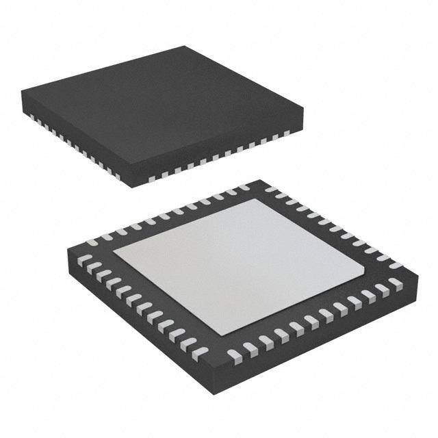
| 供应商器件封装 | 48-VQFN(7x7) |
| 其它名称 | 296-36951-1 |
| 包装 | 剪切带 (CT) |
| 商标 | Texas Instruments |
| 商标名 | MSP430 |
| 处理器系列 | 4 Series |
| 外设 | 欠压检测/复位,LCD,POR,PWM,WDT |
| 定时器数量 | 2 Timer |
| 封装 | Reel |
| 封装/外壳 | 48-VFQFN 裸露焊盘 |
| 封装/箱体 | VQFN-48 |
| 工作温度 | -40°C ~ 85°C |
| 工厂包装数量 | 250 |
| 振荡器类型 | 内部 |
| 数据总线宽度 | 16 bit |
| 数据转换器 | A/D 8x10b |
| 最大时钟频率 | 16 MHz |
| 标准包装 | 1 |
| 核心 | MSP430 |
| 核心处理器 | MSP430 |
| 核心尺寸 | 16-位 |
| 电压-电源(Vcc/Vdd) | 1.8 V ~ 3.6 V |
| 程序存储器类型 | 闪存 |
| 程序存储容量 | 16KB(16K x 8 + 256B) |
| 系列 | MSP430F4152 |
| 连接性 | I²C, IrDA, LIN, SCI, SPI, UART/USART |
| 速度 | 8MHz |


- 商务部:美国ITC正式对集成电路等产品启动337调查
- 曝三星4nm工艺存在良率问题 高通将骁龙8 Gen1或转产台积电
- 太阳诱电将投资9.5亿元在常州建新厂生产MLCC 预计2023年完工
- 英特尔发布欧洲新工厂建设计划 深化IDM 2.0 战略
- 台积电先进制程称霸业界 有大客户加持明年业绩稳了
- 达到5530亿美元!SIA预计今年全球半导体销售额将创下新高
- 英特尔拟将自动驾驶子公司Mobileye上市 估值或超500亿美元
- 三星加码芯片和SET,合并消费电子和移动部门,撤换高东真等 CEO
- 三星电子宣布重大人事变动 还合并消费电子和移动部门
- 海关总署:前11个月进口集成电路产品价值2.52万亿元 增长14.8%


PDF Datasheet 数据手册内容提取
MSP430F41x2 MIXED SIGNAL MICROCONTROLLER SLAS648E--APRIL2009--REVISEDMARCH2011 D LowSupply-VoltageRange,1.8Vto3.6V D IntegratedLCDDriverWithContrast D UltralowPowerConsumption ControlforUpto144Segments ActiveMode:220Aat1MHz,2.2V D BasicTimerWithRealTimeClockFeature StandbyMode:0.9A D Brownoutdetector OffMode(RAMRetention):0.1A D On-ChipComparatorforAnalogSignal D FivePower-SavingModes CompareFunctionorSlopeA/D D Wake-UpFromStandbyModeinLess D 10-Bit200-kspsAnalog-to-Digital(A/D) Than6s ConverterWithInternalReference, -- InternalVeryLowPower, Sample-and-Hold,Autoscan,andData Low-FrequencyOscillator TransferController D 16-BitRISCArchitecture, D SerialOnboardProgramming, 125-nsInstructionCycleTime NoExternalProgrammingVoltageNeeded D 16-BitTimer_AWithThree ProgrammableCodeProtectionbySecurity Capture/CompareRegisters Fuse D 16-BitTimer_AWithFiveCapture/Compare D BootstrapLoader Registers D On-ChipEmulationModule D TwoUniversalSerialCommunication D FamilyMembersInclude: Interfaces(USCIs) MSP430F4152: 16KB+256BFlashMemory USCI_A0 512BRAM -- EnhancedUARTSupporting MSP430F4132: 8KB+256BFlashMemory Auto-BaudrateDetection 512BRAM -- IrDAEncoderandDecoder D Availablein64-PinQFPPackageand -- SynchronousSPI 48-PinQFNPackage(SeeAvailable USCI_B0 Options) -- I2C D ForCompleteModuleDescriptions,See -- SynchronousSPI TheMSP430x4xxFamilyUser’sGuide, D SupplyVoltageSupervisor/MonitorWith LiteratureNumberSLAU056 ProgrammableLevelDetection description TheTexasInstrumentsMSP430familyofultralow-powermicrocontrollersconsistofseveraldevicesfeaturing differentsetsofperipheralstargetedforvariousapplications.Thearchitecture,combinedwithfivelowpower modes,isoptimizedtoachieveextendedbatterylifeinportablemeasurementapplications.Thedevicefeatures a powerful 16-bit RISC CPU, 16-bit registers, and constant generator that contribute to maximum code efficiency.Thedigitallycontrolledoscillator(DCO)allowswake-upfromlow-powermodestoactivemodeinless than6s. TheMSP430F41x2isamicrocontrollerconfigurationwithtwo16-bittimers,abasictimerwithareal--timeclock, a10-bitA/Dconverter,aversatileanalogcomparator,twouniversalserialcommunicationinterfaces,upto48 I/Opins,andaliquidcrystaldisplaydriver. Typicalapplicationsforthisdeviceincludeanaloganddigitalsensorsystems,remotecontrols,thermostats, digitaltimers,hand-heldmeters,etc. This integrated circuit can be damaged by ESD. Texas Instruments recommends that all integrated circuits be handled with appropriateprecautions.Failuretoobserveproperhandlingandinstallationprocedurescancausedamage.ESDdamagecanrange fromsubtleperformancedegradationtocompletedevicefailure.Precisionintegratedcircuitsmaybemoresusceptibletodamage becauseverysmallparametricchangescouldcausethedevicenottomeetitspublishedspecifications.Thesedeviceshavelimited built-inESDprotection. Please be aware that an important notice concerning availability, standard warranty, and use in critical applications of TexasInstrumentssemiconductorproductsanddisclaimerstheretoappearsattheendofthisdatasheet. PRODUCTION DATA information is current as of publication date. Copyright2011,TexasInstrumentsIncorporated ProductsconformtospecificationsperthetermsofTexasInstruments standardwarranty.Productionprocessingdoesnotnecessarilyinclude testingofallparameters. POSTOFFICEBOX655303DALLAS,TEXAS75265 1
MSP430F41x2 MIXED SIGNAL MICROCONTROLLER SLAS648E--APRIL2009--REVISEDMARCH2011 AVAILABLEOPTIONS† PACKAGEDDEVICES‡ TTA PLASTIC64-PINQFP(PM) PLASTIC48-PINQFN(RGZ) MSP430F4152IPM MSP430F4152IRGZ --40Cto85C MSP430F4132IPM MSP430F4132IRGZ †For the most current package and ordering information, see the Package Option Addendumattheendofthisdocument,orseetheTIwebsiteatwww.ti.com. ‡Package drawings, thermal data, and symbolization are available at www.ti.com/packaging. DEVELOPMENT TOOL SUPPORT AllMSP430 microcontrollers include an Embedded Emulation Module (EEM) allowing advanced debugging and programming through easy to use development tools. Recommended hardware options include the following: D DebuggingandProgrammingInterface -- MSP-FET430UIF(USB) -- MSP-FET430PIF(ParallelPort) D DebuggingandProgrammingInterfacewithTargetBoard -- MSP-FET430U64A(PMpackage) D ProductionProgrammer -- MSP-GANG430 2 POSTOFFICEBOX655303DALLAS,TEXAS75265
MSP430F41x2 MIXED SIGNAL MICROCONTROLLER SLAS648E--APRIL2009--REVISEDMARCH2011 pin designation, MSP430F41x2IPM (QFP) 8 2 0 S A1.2/A2/CA4 A1.3/A1/CA3A1.4/A0/CA2SBWTCLKMI/SBWTDIOCK/S35MS/S34DI/TCLK/S33DO/TDI/S32A0.0/S31A0.0/MCLK/S3A0.1/S29A1.0/SVSOUT/A1.0/S27 VCC6.0/TVSS7.5/T7.4/TEST/ST/N7.3/T7.2/T7.1/T7.0/T1.0/T1.1/T1.2/T1.3/T1.4/T APAPPTRPPPPPPPPP 64636261605958575655545352515049 P6.1/UCB0SOMI/UCB0SCL 1 48 P1.5/TA0CLK/CAOUT/S26 P6.2/UCB0SIMO/UCB0SDA 2 47 P1.6/ACLK/CA0 P6.3/UCB0STE/UCA0CLK/A3/CA5/VeREF-/VREF- 3 46 P1.7/TA0CLK/CAOUT/CA1 P6.4/UCB0CLK/UCA0STE/A4/CA6/VeREF+/VREF+ 4 45 P7.6/TA0.2/S25 P6.5/UCA0RXD/UCA0SOMI/A5 5 44 P5.0/TA1.1/S24 P6.6/UCA0TXD/UCA0SIMO/A6 6 43 R33/LCDCAP DVCC 7 42 P5.1/R23 64-pin XIN 8 41 P5.2/R13/LCDREF PM PACKAGE XOUT 9 40 P5.3/R03 (TOP VIEW) DVSS 10 39 P5.4/COM3 P6.7/A7/CA7/SVSIN 11 38 P5.5/COM2 P4.7/ADC10CLK/S0 12 37 P5.6/COM1 P4.6/S1 13 36 P5.7/COM0 P4.5/S2 14 35 P3.0/TA1.2/S23 P4.4/S3 15 34 P3.1/TA1.3/S22 P4.3/S4 16 33 P3.2/TA1.4/S21 17181920212223242526272829303132 5 678901234567890 S SSSS11111111112 P4.2/ P4.1/P4.0/P2.7/P2.6/2.5/S2.4/S1.4/S1.3/S1.2/S1.1/S3.7/S3.6/S3.5/SUT/SLK/S PPAAAAPPPOC TTTT A1 P2.3/P2.2/P2.1/P2.0/ P3.4/CA0.0/TA T 3/ 3. P POSTOFFICEBOX655303DALLAS,TEXAS75265 3
MSP430F41x2 MIXED SIGNAL MICROCONTROLLER SLAS648E--APRIL2009--REVISEDMARCH2011 pin designation, MSP430F41x2IRGZ (QFN)† A1.2/A2/CA4 A1.3/A1/CA3 A1.4/A0/CA2 SBWTCLK MI/SBWTDIO CK/S35 MS/S34 DI/TCLK/S33 DO/TDI/S32 A0.0/S31 VCC 6.0/T VSS 7.5/T 7.4/T EST/ ST/N 7.3/T 7.2/T 7.1/T 7.0/T 1.0/T A P A P P T R P P P P P 484746454443424140393837 P6.1 1 36 P1.1/TA0.0/MCLK/S30 P6.2 2 35 P1.5/TA0CLK/CAOUT/S26 DV 3 34 P1.6/ACLK/CA0 CC XIN 4 33 P1.7/TA0CLK/CAOUT/CA1 XOUT 5 32 R33/LCDCAP 48-pin DV 6 31 P5.1/R23 SS RGZ PACKAGE P6.7/A7/CA7/SVSIN 7 (TOP VIEW) 30 P5.2/R13/LCDREF P4.7/ADC10CLK/S0 8 29 P5.3/R03 P4.6/S1 9 28 P5.4/COM3 P4.5/S2 10 27 P5.5/COM2 P4.4/S3 11 26 P5.6/COM1 P4.3/S4 12 25 P5.7/COM0 131415161718192021222324 5 6 7 8 9 0 1 2 3 4 5 9 S S S S S 1 1 1 1 1 1 1 P4.2/ P4.1/ P4.0/ P2.7/ P2.6/ 2.5/S 2.4/S 1.4/S 1.3/S 1.2/S 1.1/S UT/S P P A A A A O T T T T A 3/ 2/ 1/ 0/ C 2. 2. 2. 2. 4/ P P P P 3. P †“Notavailable”pinsinthe48-pinpackageshouldbeinitializedtooutputdirection. 4 POSTOFFICEBOX655303DALLAS,TEXAS75265
MSP430F41x2 MIXED SIGNAL MICROCONTROLLER SLAS648E--APRIL2009--REVISEDMARCH2011 functional block diagram XIN XOUT DVCC DVSS AVCC AVSS P1.x/P2.x P3.x/P4.x P5.x/P6.x P7.x 2x8 2x8 2x8 1x7 ACLK Oscillators ADC10 USCIA0 Ports FLL+ SMCLK Flash RAM UART/ P1/P2 Ports Ports Port VLO 10--bit LIN, P3/P4 P5/P6 P7 IrDA,SPI 16kB 512B 8Channels 2x8I/O 2x8I/O 2x8I/O 1x7I/O MCLK 8kB 512B Autoscan USCIB0 Interrupt DTC SPI,I2C capability CPU MAB 64kB incl.16 Registers MDB EEM Brownout LCD_A Basic Watchdog Timer_A3 Timer_A5 Protection 144 Timer& Comparator WDT+ Segments Real-- JTAG _A+ 3CC 5CC SVS, 1,2,3,4 Time Interface 15--Bit Registers Registers SVM Mux Clock Spy--Bi-- Wire RST/NMI NOTE: TheUSCIA0andUSCIB0cannotbeusedinthe48-pinpackageoptions(RGZ). POSTOFFICEBOX655303DALLAS,TEXAS75265 5
MSP430F41x2 MIXED SIGNAL MICROCONTROLLER SLAS648E--APRIL2009--REVISEDMARCH2011 Terminal Functions TERMINAL NO. II//OO DDEESSCCRRIIPPTTIIOONN NAME 64 48 PIN PIN General-purposedigitalI/Opin P1.0/TA0.0/S31 53 37 I/O Timer0_A3,capture:CCI0Ainput,compare:Out0output LCDsegmentoutput General-purposedigitalI/Opin P1.1/TA0.0/ Timer0_A3,capture:CCI0Binput 52 36 I/O MCLK/S30 MCLKsignaloutput LCDsegmentoutput General-purposedigitalI/Opin P1.2/TA0.1/S29 51 -- I/O Timer0_A3,capture:CCI1Ainput,compare:Out1output LCDsegmentoutput General-purposedigitalI/Opin P1.3/TA1.0/ Timer1_A5,capture:CCI0Binput 50 -- I/O SVSOUT/S28 SVScomparatoroutput LCDsegmentoutput General-purposedigitalI/Opin/ P1.4/TA1.0/S27 49 -- I/O Timer1_A5,capture:CCI0Ainput,compare:Out0output LCDsegmentoutput General-purposedigitalI/Opin P1.5/TA0CLK/ Timer0_A3,clocksignalTACLKinput 48 35 I/O CAOUT/S26 Comparator_Aoutput LCDsegmentoutput General-purposedigitalI/Opin P1.6/ACLK/CA0 47 34 I/O Comparator_Ainput0 ACLKsignaloutput General-purposedigitalI/Opin P1.7/TA0CLK Timer0_A3,clocksignalTACLKinput 46 33 I/O CAOUT/CA1 Comparator_Aoutput Comparator_Ainput1 General-purposedigitalI/Opin P2.0/TA1.1/S15 27 23 I/O Timer1_A5,compare:Out1Output LCDsegmentoutput General-purposedigitalI/Opin P2.1/TA1.2/S14 26 22 I/O Timer1_A5,compare:Out2Output LCDsegmentoutput General-purposedigitalI/Opin P2.2/TA1.3/S13 25 21 I/O Timer1_A5,compare:Out3Output LCDsegmentoutput General-purposedigitalI/Opin P2.3/TA1.4/S12 24 20 I/O Timer1_A5,compare:Out4output LCDsegmentoutput General-purposedigitalI/Opin P2.4/S11 23 19 I/O LCDsegmentoutput General-purposedigitalI/Opin P2.5/S10 22 18 I/O LCDsegmentoutput General-purposedigitalI/Opin P2.6/S9 21 17 I/O LCDsegmentoutput General-purposedigitalI/Opin P2.7/S8 20 16 I/O LCDsegmentoutput 6 POSTOFFICEBOX655303DALLAS,TEXAS75265
MSP430F41x2 MIXED SIGNAL MICROCONTROLLER SLAS648E--APRIL2009--REVISEDMARCH2011 Terminal Functions (continued) TERMINAL NO. II//OO DDEESSCCRRIIPPTTIIOONN NAME 64 48 PIN PIN General-purposedigitalI/Opin P3.0/TA1.2/S23 35 -- I/O Timer1_A5,capture:CCI2Ainput,compare:Out2output LCDsegmentoutput General-purposedigitalI/Opin P3.1/TA1.3/S22 34 -- I/O Timer1_A5,capture:CCI3Ainput,compare:Out3output LCDsegmentoutput General-purposedigitalI/Opin P3.2/TA1.4/S21 33 -- I/O Timer1_A5,capture:CCI4Ainput,compare:Out4output LCDsegmentoutput General-purposedigitalI/Opin P3.3/TA0.0/ Timer0_A3,compare:Out0output 32 -- I/O TA1CLK/S20 Timer1_A5,clocksignalTACLKinput LCDsegmentoutput General-purposedigitalI/Opin P3.4/CAOUT/S19 31 24 I/O Comparator_Aoutput LCDsegmentoutput General-purposedigitalI/Opin P3.5/S18 30 -- I/O LCDsegmentoutput General-purposedigitalI/Opin P3.6/S17 29 -- I/O LCDsegmentoutput General-purposedigitalI/Opin P3.7/S16 28 -- I/O LCDsegmentoutput General-purposedigitalI/Opin P4.0/S7 19 15 I/O LCDsegmentoutput General-purposedigitalI/Opin P4.1/S6 18 14 I/O LCDsegmentoutput General-purposedigitalI/Opin P4.2/S5 17 13 I/O LCDsegmentoutput General-purposedigitalI/Opin P4.3/S4 16 12 I/O LCDsegmentoutput General-purposedigitalI/Opin P4.4/S3 15 11 I/O LCDsegmentoutput General-purposedigitalI/Opin P4.5/S2 14 10 I/O LCDsegmentoutput General-purposedigitalI/Opin P4.6/S1 13 9 I/O LCDsegmentoutput General-purposedigitalI/Opin P4.7/ADC10CLK/ 12 8 I/O ADC10,conversionclock S0 LCDsegmentoutput General-purposedigitalI/Opin P5.0/TA1.1/S24 44 -- I/O Timer1_A5,capture:CCI1Ainput,compare:Out1output LCDsegmentoutput CapacitorconnectionforLCDchargepump LCDCAP/R33 43 32 I/O inputportofthemostpositiveanalogLCDlevel(V4) General-purposedigitalI/Opin P5.1/R23 42 31 I/O inputportofthesecondmostpositiveanalogLCDlevel(V3) General-purposedigitalI/Opin P5.2/LCDREF/ 41 30 I/O ExternalLCDreferencevoltageinput R13 inputportofthethirdmostpositiveanalogLCDlevel(V3orV2) POSTOFFICEBOX655303DALLAS,TEXAS75265 7
MSP430F41x2 MIXED SIGNAL MICROCONTROLLER SLAS648E--APRIL2009--REVISEDMARCH2011 Terminal Functions (continued) TERMINAL NO. II//OO DDEESSCCRRIIPPTTIIOONN NAME 64 48 PIN PIN General-purposedigitalI/Opin P5.3/R03 40 29 I/O inputportofthefourthmostpositiveanalogLCDlevel(V1) General-purposedigitalI/Opin P5.4/COM3 39 28 I/O commonoutput,COM0--3areusedforLCDbackplanes General-purposedigitalI/Opin P5.5/COM2 38 27 I/O commonoutput,COM0--3areusedforLCDbackplanes General-purposedigitalI/Opin P5.6/COM1 37 26 I/O commonoutput,COM0--3areusedforLCDbackplanes General-purposedigitalI/Opin P5.7/COM0 36 25 I/O commonoutput,COM0--3areusedforLCDbackplanes General-purposedigitalI/Opin P6.0/TA1.2/A2†/ Timer1_A5,compare:Out2output 63 47 I/O CA4 ADC10analoginputA2† Comparator_Ainput4 P6.1/ General-purposedigitalI/Opin UCB0SOMI†/ 1 1 I/O USCIB0slaveout/masterininSPImode,SCLI2CclockinI2Cmode† UCB0SCL† P6.2/ General-purposedigitalI/Opin UCB0SIMO†/ 2 2 I/O USCIB0slavein/masteroutinSPImode,SDAI2CdatainI2Cmode† UCB0SDA† General-purposedigitalI/Opin P6.3/UCB0STE/ USCIB0slavetransmitenable/USCIA0clockinput/output UCA0CLK/A3/ 3 -- I/O ADC10analoginputA3/negativereference CA5/Veref--/Vref-- Comparator_Ainput5 General-purposedigitalI/Opin P6.4/UCB0CLK/ USCIB0clockinput/output,USCIA0slavetransmitenable UCA0STE/A4/ 4 -- I/O ADC10analoginputA4/positivereference CA6/Veref+/Vref+ Comparator_Ainput6 General-purposedigitalI/Opin P6.5/UCA0RXD/ 5 -- I/O USCIA0receivedatainputinUARTmode,slavedataout/masterininSPImode UCA0SOMI/A5 ADC10analoginputA5 General-purposedigitalI/Opin P6.6/UCA0TXD/ 6 -- I/O USCIA0transmitdataoutputinUARTmode,slavedatain/masteroutSPImode UCA0SIMO/A6 ADC10analoginputA6 General-purposedigitalI/Opin P6.7/A7/CA7/ ADC10analoginputA7 11 7 I/O SVSIN Comparator_Ainput7 SVSinput P7.0/TDO/TDI/ 54 38 I/O General-purposedigitalI/Opin S32 JTAGtestdataoutputterminalortestdatainputinprogrammingantest LCDsegmentoutput P7.1/TDI/TCLK/ 55 39 I/O General-purposedigitalI/Opin S33 JTAGtestdatainputortestclockinputinprogrammingantest LCDsegmentoutput P7.2/TMS/S34 56 40 I/O General-purposedigitalI/Opin JTAGtestmodeselect,inputterminalfordeviceprogrammingandtest LCDsegmentoutput †64-pinpackagedevicesonly 8 POSTOFFICEBOX655303DALLAS,TEXAS75265
MSP430F41x2 MIXED SIGNAL MICROCONTROLLER SLAS648E--APRIL2009--REVISEDMARCH2011 Terminal Functions (continued) TERMINAL NO. II//OO DDEESSCCRRIIPPTTIIOONN NAME 64 48 PIN PIN P7.3/TCK/S35 57 41 I/O General-purposedigitalI/Opin Testclockinputfordeviceprogrammingandtest LCDsegmentoutput General-purposedigitalI/Opin P7.4/TA1.4/ Timer1_A5,capture:CCI4Binput,compare:Out4output 60 44 I/O A0/CA2 ADC10analoginputA0 Comparator_Ainput2 General-purposedigitalI/Opin P7.5/TA1.3/ Timer1_A5,capture:CCI3Binput,compare:Out3output 61 45 I/O A1/CA3 ADC10analoginputA1 Comparator_Ainput3 General-purposedigitalI/Opin P7.6/TA0.2/S25 45 -- I/O Timer0_A3,capture:CCI2Ainput,compare:Out2output LCDsegmentoutput AVCC 64 48 Analogsupplyvoltage,positiveterminal AVSS 62 46 Analogsupplyvoltage,negativeterminal DVCC 7 3 Digitalsupplyvoltage,positiveterminal.Suppliesalldigitalparts. DVSS 10 6 Digitalsupplyvoltage,negativeterminal.Suppliesalldigitalparts. XOUT 9 5 O OutputportforcrystaloscillatorXT1.Standardorwatchcrystalscanbeconnected. XIN 8 4 I InputportforcrystaloscillatorXT1.Standardorwatchcrystalscanbeconnected. RST/NMI/ 58 42 I Resetornonmaskableinterruptinput SBWTDIO Spy-Bi-Wiretestdatainput/outputduringprogrammingandtest TEST/SBWTCLK 59 43 I SelectstestmodeforJTAGpinsonPort7.ThedeviceprotectionfuseisconnectedtoTEST. ThermalPad NA NA NA QFNpackagepad(RGZpackageonly).ConnectiontoDVSSisrecommended. POSTOFFICEBOX655303DALLAS,TEXAS75265 9
MSP430F41x2 MIXED SIGNAL MICROCONTROLLER SLAS648E--APRIL2009--REVISEDMARCH2011 short-form description CPU TheMSP430CPUhasa16-bitRISCarchitecture ProgramCounter PC/R0 that is highly transparent to the application. All operations,otherthanprogram-flowinstructions, StackPointer SP/R1 are performed as register operations in StatusRegister SR/CG1/R2 conjunction with seven addressing modes for source operand and four addressing modes for ConstantGenerator CG2/R3 destinationoperand. General-PurposeRegister R4 The CPU is integrated with 16 registers that provide reduced instruction execution time. The General-PurposeRegister R5 register-to-register operation execution time is onecycleoftheCPUclock. General-PurposeRegister R6 Fouroftheregisters,R0toR3,arededicatedas General-PurposeRegister R7 program counter, stack pointer, status register, and constant generator, respectively. The General-PurposeRegister R8 remaining registers are general-purpose registers. General-PurposeRegister R9 PeripheralsareconnectedtotheCPUusingdata, General-PurposeRegister R10 address, and control buses and can be handled withallinstructions. General-PurposeRegister R11 instructionset General-PurposeRegister R12 Theinstructionsetconsistsof51instructionswith three formats and seven address modes. Each General-PurposeRegister R13 instruction can operate on word and byte data. Table1 shows examples of the three types of General-PurposeRegister R14 instruction formats; Table 2 shows the address General-PurposeRegister R15 modes. Table1.InstructionWordFormats Dualoperands,source-destination e.g.,ADD R4,R5 R4+R5------>R5 Singleoperands,destinationonly e.g.,CALL R8 PC---->(TOS),R8---->PC Relativejump,un/conditional e.g.,JNE Jump-on-equalbit=0 Table2.AddressModeDescriptions ADDRESSMODE S D SYNTAX EXAMPLE OPERATION Register F F MOVRs,Rd MOVR10,R11 R10—>R11 Indexed F F MOVX(Rn),Y(Rm) MOV2(R5),6(R6) M(2+R5)—>M(6+R6) Symbolic(PCrelative) F F MOVEDE,TONI M(EDE)—>M(TONI) Absolute F F MOV&MEM,&TCDAT M(MEM)—>M(TCDAT) Indirect F MOV@Rn,Y(Rm) MOV@R10,Tab(R6) M(R10)—>M(Tab+R6) Indirect M(R10)—>R11 F MOV@Rn+,Rm MOV@R10+,R11 autoincrement R10+2—>R10 Immediate F MOV#X,TONI MOV#45,TONI #45—>M(TONI) NOTE: S=source,D=destination 10 POSTOFFICEBOX655303DALLAS,TEXAS75265
MSP430F41x2 MIXED SIGNAL MICROCONTROLLER SLAS648E--APRIL2009--REVISEDMARCH2011 operatingmodes TheMSP430hasoneactivemodeandfivesoftwareselectablelow-powermodesofoperation.Aninterrupt eventcanwakeupthedevicefromanyofthefivelow-powermodes,servicetherequest,andrestorebackto thelow-powermodeonreturnfromtheinterruptprogram. Thefollowingsixoperatingmodescanbeconfiguredbysoftware: D Activemode(AM) -- Allclocksareactive D Low-powermode0(LPM0) -- CPUisdisabled -- ACLKandSMCLKremainactive -- FLL+loopcontrolremainsactive D Low-powermode1(LPM1) -- CPUisdisabled -- ACLKandSMCLKremainactive -- FLL+loopcontrolisdisabled D Low-powermode2(LPM2) -- CPUisdisabled -- MCLK,FLL+loopcontrol,andDCOCLKaredisabled -- DCO’sdcgeneratorremainsenabled -- ACLKremainsactive D Low-powermode3(LPM3) -- CPUisdisabled -- MCLK,FLL+loopcontrol,andDCOCLKaredisabled -- DCO’sdcgeneratorisdisabled -- ACLKremainsactive D Low-powermode4(LPM4) -- CPUisdisabled -- ACLKisdisabled -- MCLK,FLL+loopcontrol,andDCOCLKaredisabled -- DCO’sdcgeneratorisdisabled -- Crystaloscillatorisstopped POSTOFFICEBOX655303DALLAS,TEXAS75265 11
MSP430F41x2 MIXED SIGNAL MICROCONTROLLER SLAS648E--APRIL2009--REVISEDMARCH2011 interruptvectoraddresses Theinterruptvectorsandthepower-upstartingaddressarelocatedintheaddressrange0xFFFFto0xFFC0. Thevectorcontainsthe16-bitaddressoftheappropriateinterrupt-handlerinstructionsequence. Iftheresetvector(locatedataddress0xFFFE)contains0xFFFF(e.g.,flashisnotprogrammed),theCPUgoes intoLPM4immediatelyafterpower-up. WORD INTERRUPTSOURCE INTERRUPTFLAG SYSTEMINTERRUPT PRIORITY ADDRESS Power-Up PORIFG ExternalReset RSTIFG Watchdog WDTIFG Reset 0xFFFE 15,highest FlashMemory KEYV PCOut--of--Range(seeNote4) (seeNote1) NMI NMIIFG(seeNotes1and3) (Non)maskable OscillatorFault OFIFG(seeNotes1and3) (Non)maskable 0xFFFC 14 FlashMemoryAccessViolation ACCVIFG(seeNotes1,2,and4) (Non)maskable Timer_A5 TA1CCR0CCIFG0(seeNote2) Maskable 0xFFFA 13 TA1CCR1toTACCR4CCIFGs, Timer_A5 Maskable 0xFFF8 12 andTAIFG(seeNotes1and2) Comparator_A+ CAIFG Maskable 0xFFF6 11 WatchdogTimer+ WDTIFG Maskable 0xFFF4 10 UCA0RXIFG(seeNote1), UCB0RXIFG(SPImode),or USCI_A0/B0Receive UCB0STATUCALIFG,UCNACKIFG,UCSTTIFG, Maskable 0xFFF2 9 UCSTPIFG(I2Cmode) (seeNote1) UCA0TXIFG(seeNote1), UCB0TXIFG(SPImode),or USCI_A0/B0Transmit Maskable 0xFFF0 8 UCB0RXIFGandUCB0TXIFG(I2Cmode) (seeNote1) ADC10 ADC10IFG(seeNote2) Maskable 0xFFEE 7 Timer_A3 TACCR0CCIFG0(seeNote2) Maskable 0xFFEC 6 TACCR1CCIFG1andTACCR2CCIFG2, Timer_A3 Maskable 0xFFEA 5 TAIFG(seeNotes1and2) I/OPortP1(EightFlags) P1IFG.0toP1IFG.7(seeNotes1and2) Maskable 0xFFE8 4 0xFFE6 3 0xFFE4 2 I/OPortP2(EightFlags) P2IFG.0toP2IFG.7(seeNotes1and2) Maskable 0xFFE2 1 BasicTimer1/RTC BTIFG Maskable 0xFFE0 0,lowest NOTES: 1. Multiplesourceflags 2. Interruptflagsarelocatedinthemodule. 3. AresetisgeneratediftheCPUtriestofetchinstructionsfromwithinthemoduleregistermemoryaddressrange(0hto01FFh). (Non)maskable:theindividualinterrupt-enablebitcandisableaninterruptevent,butthegeneral-interruptenablecannotdisableit. 4. Accessandkeyviolations,KEYVandACCVIFG. 12 POSTOFFICEBOX655303DALLAS,TEXAS75265
MSP430F41x2 MIXED SIGNAL MICROCONTROLLER SLAS648E--APRIL2009--REVISEDMARCH2011 special function registers Mostinterruptandmodule-enablebitsarecollectedinthelowestaddressspace.Special-functionregisterbits notallocatedtoafunctionalpurposearenotphysicallypresentinthedevice.Thisarrangementprovidessimple softwareaccess. interruptenable1and2 Address 7 6 5 4 3 2 1 0 00h ACCVIE NMIIE OFIE WDTIE rw--0 rw--0 rw--0 rw--0 WDTIE Watchdogtimerinterruptenable.Inactiveifwatchdogmodeisselected.Activeifwatchdog timerisconfiguredinintervaltimermode. OFIE Oscillatorfaultenable NMIIE (Non)maskableinterruptenable ACCVIE Flashaccessviolationinterruptenable Address 7 6 5 4 3 2 1 0 01h BTIE UCB0TXIE UCB0RXIE UCA0TXIE UCA0RXIE rw--0 rw--0 rw--0 rw--0 rw--0 UCA0RXIE USCI_A0receiveinterruptenable UCA0TXIE USCI_A0transmitinterruptenable UCB0RXIE USCI_B0receiveinterruptenable UCB0TXIE USCI_B0transmitinterruptenable BTIE Basictimerinterruptenable POSTOFFICEBOX655303DALLAS,TEXAS75265 13
MSP430F41x2 MIXED SIGNAL MICROCONTROLLER SLAS648E--APRIL2009--REVISEDMARCH2011 interruptflagregister1and2 Address 7 6 5 4 3 2 1 0 02h NMIIFG RSTIFG PORIFG OFIFG WDTIFG rw--0 rw--(0) rw--(1) rw--1 rw--(0) WDTIFG Setonwatchdogtimeroverflow(inwatchdogmode)orsecuritykeyviolation. ResetonV power-uporaresetconditionatRST/NMIpininresetmode. CC OFIFG Flagsetonoscillatorfault RSTIFG Externalresetinterruptflag.SetonaresetconditionatRST/NMIpininresetmode.Reset onV power-up. CC PORIFG Power-oninterruptflag.SetonV power--up. CC NMIIFG SetviaRST/NMI-pin Address 7 6 5 4 3 2 1 0 UCB0 UCB0 UCA0 UCA0 03h BTIFG TXIFG RXIFG TXIFG RXIFG rw--0 rw--1 rw--0 rw--1 rw--0 UCA0RXIFG USCI_A0receiveinterruptflag UCA0TXIFG USCI_A0transmitinterruptflag UCB0RXIFG USCI_B0receiveinterruptflag UCB0TXIFG USCI_B0transmitinterruptflag BTIFG BasicTimer1interruptflag Legend rw: Bitcanbereadandwritten. rw-0,1: Bitcanbereadandwritten.ItisResetorsetbyPUC. rw-(0,1): Bitcanbereadandwritten.ItisResetorsetbyPOR. SFRbitisnotpresentindevice 14 POSTOFFICEBOX655303DALLAS,TEXAS75265
MSP430F41x2 MIXED SIGNAL MICROCONTROLLER SLAS648E--APRIL2009--REVISEDMARCH2011 memory organization MSP430F4152 MSP430F4132 Memory Size 16KB 8KB Main:interruptvector Flash 0FFFFh--0FFE0h 0FFFFh--0FFE0h Main:codememory Flash 0FFFFh--0C000h 0FFFFh--0E000h Informationmemory Size 256Byte 256Byte Flash 010FFh--01000h 010FFh--01000h Bootmemory Size 1KB 1KB ROM 0FFFh--0C00h 0FFFh--0C00h RAM Size 512B 512B 03FFh--0200h 03FFh--0200h Peripherals 16-bit 01FFh--0100h 01FFh--0100h 8-bit 0FFh--010h 0FFh--010h 8-bitSFR 0Fh--00h 0Fh--00h bootstrap loader (BSL) TheMSP430BSLenablesuserstoprogramtheflashmemoryorRAMusingaUARTserialinterface.Access totheMSP430memoryviatheBSLisprotectedbyuser-definedpassword.Forcompletedescriptionofthe featuresoftheBSLanditsimplementation,seetheMSP430MemoryProgrammingUser’sGuide,literature numberSLAU265. BSLFUNCTION PMPACKAGEPINS RGZPACKAGEPINS Datatransmit 53--P1.0 37--P1.0 Datareceive 52--P1.1 36--P1.1 flash memory (Flash) TheflashmemorycanbeprogrammedviatheJTAGport,thebootstraploader,orin-systembytheCPU.The CPUcanperformsingle-byteandsingle-wordwritestotheflashmemory.Featuresoftheflashmemoryinclude: D Flash memory has n segments of main memory and four segments of information memory (A to D) of 64byteseach.Eachsegmentinmainmemoryis512bytesinsize. D Segments0tonmaybeerasedinonestep,oreachsegmentmaybeindividuallyerased. D SegmentsAtoDcanbeerasedindividually,orasagroupwithsegments0ton. SegmentsAtoDarealsocalledinformationmemory. POSTOFFICEBOX655303DALLAS,TEXAS75265 15
MSP430F41x2 MIXED SIGNAL MICROCONTROLLER SLAS648E--APRIL2009--REVISEDMARCH2011 peripherals PeripheralsareconnectedtotheCPUthroughdata,address,andcontrolbusesandcanbehandledusingall instructions.Forcompletemoduledescriptions,seetheMSP430x4xxFamilyUser’sGuide,literaturenumber SLAU056. oscillator and system clock TheclocksystemintheMSP430F41x2issupportedbytheFLL+modulethatincludessupportfora32768-Hz watch crystal oscillator, an internal very low-power low--frequency oscillator, an internal digitally-controlled oscillator(DCO),andan8-MHzhigh-frequencycrystaloscillator(XT1).TheFLL+clockmoduleisdesignedto meet the requirements of both low system cost and low power consumption. The FLL+ features a digital frequencylockedloop(FLL)hardwarethat,inconjunctionwithadigitalmodulator,stabilizestheDCOfrequency to a programmable multiple of the watch crystal frequency. The internal DCO provides a fast turn-on clock sourceandstabilizesinlessthan6s.TheFLL+moduleprovidesthefollowingclocksignals: D Auxiliary clock (ACLK), sourced from a 32768-Hz watch crystal, a high-frequency crystal, or a very low-powerLFoscillator D Mainclock(MCLK),thesystemclockusedbytheCPU D Sub-Mainclock(SMCLK),thesub-systemclockusedbytheperipheralmodules D ACLK/n,thebufferedoutputofACLK,ACLK/2,ACLK/4,orACLK/8 brownout, supply voltage supervisor Thebrownoutcircuitisimplementedtoprovidetheproperinternalresetsignaltothedeviceduringpoweron andpoweroff.Thesupplyvoltagesupervisor(SVS)circuitrydetectsifthesupplyvoltagedropsbelowauser selectablelevelandsupportsbothsupplyvoltagesupervision(thedeviceisautomaticallyreset)andsupply voltagemonitoring(SVM,thedeviceisnotautomaticallyreset). TheCPUbeginscodeexecutionafterthebrownoutcircuitreleasesthedevicereset.However,V maynot CC haverampedtoV atthattime.TheusermustinsurethedefaultFLL+settingsarenotchangeduntilV CC(min) CC reachesV .Ifdesired,theSVScircuitcanbeusedtodeterminewhenV reachesV . CC(min) CC CC(min) digital I/O Thereareseven8-bitI/Oportsimplemented—portsP1throughP7.PortP7isa7-bitI/Oport. D AllindividualI/Obitsareindependentlyprogrammable. D Anycombinationofinput,output,andinterruptconditionsispossible. D Edge-selectableinterruptinputcapabilityforalltheeightbitsofportsP1andP2. D Read/writeaccesstoport-controlregistersissupportedbyallinstructions. 16 POSTOFFICEBOX655303DALLAS,TEXAS75265
MSP430F41x2 MIXED SIGNAL MICROCONTROLLER SLAS648E--APRIL2009--REVISEDMARCH2011 watchdog timer (WDT+) TheprimaryfunctionoftheWDT+moduleistoperformacontrolledsystemrestartafterasoftwareproblem occurs.Iftheselectedtimeintervalexpires,asystemresetisgenerated.Ifthewatchdogfunctionisnotneeded inanapplication,themodulecanbeconfiguredasanintervaltimerandcangenerateinterruptsatselectedtime intervals. Basic Timer1 and Real-Time Clock (RTC) TheBasicTimer1hastwoindependent8-bittimerswhichcanbecascadedtoforma16-bittimer/counter.Both timerscanbereadandwrittenbysoftware.TheBasicTimer1isextendedtoprovideanintegratedreal-time clock (RTC). An internal calendar compensates for month with less than 31 days and includes leap year correction. LCD_A driver with regulated charge pump TheLCD_AdrivergeneratesthesegmentandcommonsignalsrequiredtodriveanLCDdisplay.TheLCD_A controllerhasdedicateddatamemorytoholdsegmentdriveinformation.Commonandsegmentsignalsare generatedasdefinedbythemode.Static,2--MUX,3--MUX,and4--MUXLCDsaresupportedbythisperipheral. The module can provide a LCD voltage independent of the supply voltage via an integrated charge pump. FurthermoreitispossibletocontroltheleveloftheLCDvoltageandthuscontrastinsoftware. Timer0_A3 Timer_A3 is a 16-bit timer/counter with three capture/compare registers. Timer_A3 can support multiple capture/compares, PWM outputs, and interval timing. Timer_A3 also has extensive interrupt capabilities. Interruptsmaybegeneratedfromthecounteronoverflowconditionsandfromeachofthecapture/compare registers. TIMER_A3SIGNALCONNECTIONS INPUTPINNUMBER MODULE OUTPUTPINNUMBER DDEEVVIICCEEIINNPPUUTT MMOODDUULLEE MMOODDUULLEE OOUUTTPPUUTT SIGNAL INPUTNAME BLOCK PM RGZ SIGNAL PM RGZ 48--P1.5 35--P1.5 TA0CLK TACLK 46--P1.7 33--P1.7 ACLK ACLK TTiimmeerr NNAA SMCLK SMCLK 48--P1.5 35--P1.5 TA0CLK TACLK 53--P1.0 37--P1.0 TA0.0 CCI0A 53--P1.0 37--P1.0 52--P1.1 36--P1.1 TA0.0 CCI0B 32--P3.3 -- CCCCRR00 TTAA00 DVSS GND DVCC VCC 51--P1.2 -- TA0.1 CCI1A 51--P1.2 CAOUT(internal) CCI1B ADC10(internal) ADC10(internal) CCCCRR11 TTAA11 DVSS GND DVCC VCC 45--P7.6 -- TA0.2 CCI2A 45--P7.6 -- ACLK(internal) CCI2B CCCCRR22 TTAA22 DVSS GND DVCC VCC POSTOFFICEBOX655303DALLAS,TEXAS75265 17
MSP430F41x2 MIXED SIGNAL MICROCONTROLLER SLAS648E--APRIL2009--REVISEDMARCH2011 Timer1_A5 Timer_A5 is a 16-bit timer/counter with five capture/compare registers. Timer_A5 can support multiple capture/compares, PWM outputs, and interval timing. Timer_A5 also has extensive interrupt capabilities. Interruptsmaybegeneratedfromthecounteronoverflowconditionsandfromeachofthecapture/compare registers. TIMER_A5SIGNALCONNECTIONS INPUTPINNUMBER MODULE OUTPUTPINNUMBER DDEEVVIICCEEIINNPPUUTT MMOODDUULLEE MMOODDUULLEE OOUUTTPPUUTT SIGNAL INPUTNAME BLOCK PM RGZ SIGNAL PM RGZ 32--P3.3 -- TA1CLK TACLK ACLK ACLK TTiimmeerr NNAA SMCLK SMCLK 32--P3.3 -- TA1CLK TACLK 49--P1.4 -- TA1.0 CCI0A 49--P1.4 -- 50--P1.3 -- TA1.0 CCI0B ADC10(internal) ADC10(internal) CCCCRR00 TTAA00 DVSS GND DVCC VCC 44--P5.0 -- TA1.1 CCI1A 44--P5.0 -- CAOUT(internal) CCI1B 27--P2.0 23--P2.0 CCCCRR11 TTAA11 DVSS GND ADC10(internal) ADC10(internal) DVCC VCC 35--P3.0 -- TA1.2 CCI2A 35--P3.0 -- ACLK(internal) CCI2B 26--P2.1 22--P2.1 CCCCRR22 TTAA22 DVSS GND 63--P6.0 47--P6.0 DVCC VCC 34--P3.1 -- TA1.3 CCI3A 34--P3.1 -- 61--P7.5 45--P7.5 TA1.3 CCI3B 25--P2.2 21--P2.2 CCCCRR33 TTAA33 DVSS GND 61--P7.5 45--P7.5 DVCC VCC 33--P3.2 -- TA1.4 CCI4A 33--P3.2 -- 60--P7.4 44--P7.4 TA1.4 CCI4B 24--P2.3 20--P2.3 CCCCRR44 TTAA44 DVSS GND 60--P7.4 44--P7.4 DVCC VCC universal serial communication interface (USCI) (USCI_A0, USCI_B0) The USCI module is used for serial data communication. The USCI module supports synchronous communication protocols like SPI (3 or 4 pin), I2C and asynchronous communication protocols like UART, enhancedUARTwithautomaticbaudratedetection(LIN),andIrDA. USCI_A0providessupportforSPI(3or4pin),UART,enhancedUART,andIrDA. USCI_B0providessupportforSPI(3or4pin)andI2C. Comparator_A+ Theprimaryfunctionofthecomparator_A+moduleistosupportprecisionslopeanalog-to-digitalconversions, battery-voltagesupervision,andmonitoringofexternalanalogsignals. 18 POSTOFFICEBOX655303DALLAS,TEXAS75265
MSP430F41x2 MIXED SIGNAL MICROCONTROLLER SLAS648E--APRIL2009--REVISEDMARCH2011 ADC10 TheADC10modulesupportsfast10-bitanalog-to-digitalconversions.Themoduleimplementsa10-bitSAR core,sampleselectcontrol,referencegenerator,anddatatransfercontroller(DTC)forautomaticconversion resulthandling,allowingADCsamplestobeconvertedandstoredwithoutanyCPUintervention. peripheral file map PERIPHERALSWITHWORDACCESS Watchdog Watchdogtimercontrol WDTCTL 0120h TTiimmeerr00__AA33 CCaappttuurree//ccoommppaarreerreeggiisstteerr22 TTAA00CCCCRR22 00117766hh CCaappttuurree//ccoommppaarreerreeggiisstteerr11 TTAA00CCCCRR11 00117744hh Cappture//compparereggister0 TA0CCR0 0172h Timer__Areggister TA0R 0170h Cappture/compparecontrol2 TA0CCTL2 0166h Capture/comparecontrol1 TA0CCTL1 0164h Capture/comparecontrol0 TA0CCTL0 0162h Timer_Acontrol TA0CTL 0160h Timer_Ainterruptvector TA0IV 012Eh Timer1_A5 Capture/compareregister4 TA1CCR4 019A CCaptture//compareregiistter33 TTAA11CCCCRR33 00119988 CCaappttuurree//ccoommppaarreerreeggiisstteerr22 TTAA11CCCCRR22 00119966hh Capture/compareregister1 TA1CCR1 0194h Capture/compareregister0 TA1CCR0 0192h TTiimmeerr_AArreeggiisstteerr TTAA11RR 00119900hh Cappture/compparecontrol4 TA1CCTL4 018A Capture/comparecontrol3 TA1CCTL3 0188 CCaappttuurree//ccoommppaarreeccoonnttrrooll22 TTAA11CCCCTTLL22 00118866hh Cappture//compparecontrol1 TA1CCTL1 0184h Capture/comparecontrol0 TA1CCTL0 0182h TTiimmeerr_AAccoonnttrrooll TTAA11CCTTLL 00118800hh Timer_Ainterruptvector TA1IV 011Eh FFllaasshh FFllaasshhccoonnttrrooll33 FFCCTTLL33 001122CChh FFllaasshhccoonnttrrooll22 FFCCTTLL22 001122AAhh Flashcontrol1 FCTL1 0128h ADC10 ADCdatatransferstartaddress ADC10SA 01BCh ADCmemory ADC10MEM 01B4h ADCcontrolregister1 ADC10CTL1 01B2h ADCcontrolregister0 ADC10CTL0 01B0h ADCanalogenable0 ADC10AE0 004Ah ADCanalogenable1 ADC10AE1 004Bh ADCdatatransfercontrolregister1 ADC10DTC1 0049h ADCdatatransfercontrolregister0 ADC10DTC0 0048h POSTOFFICEBOX655303DALLAS,TEXAS75265 19
MSP430F41x2 MIXED SIGNAL MICROCONTROLLER SLAS648E--APRIL2009--REVISEDMARCH2011 peripheral file map (continued) PERIPHERALSWITHBYTEACCESS LCD_A LCDVoltageControl1 LCDAVCTL1 0AFh LCDVoltageControl0 LCDAVCTL0 0AEh LCDVoltagePortControl1 LCDAPCTL1 0ADh LCDVoltagePortControl0 LCDAPCTL0 0ACh LCDmemory20 LCDM20 0A4h : : : LCDmemory16 LCDM16 0A0h LCDmemory15 LCDM15 09Fh : : : LCDmemory1 LCDM1 091h LCDcontrolandmode LCDACTL 090h USCIA0//B0 USCIA0autobaudratecontrol UCA0ABCTL 0x005D USCIA0transmitbuffer UCA0TXBUF 0x0067 USCIA0receivebuffer UCA0RXBUF 0x0066 USCIA0status UCA0STAT 0x0065 USCIA0modulationcontrol UCA0MCTL 0x0064 USCIA0baudratecontrol1 UCA0BR1 0x0063 USCIA0baudratecontrol0 UCA0BR0 0x0062 USCIA0control1 UCA0CTL1 0x0061 USCIA0control0 UCA0CTL0 0x0060 USCIA0IrDAreceivecontrol UCA0IRRCTL 0x005F USCIA0IrDAtransmitcontrol UCA0IRTCTL 0x005E USCIB0transmitbuffer UCB0TXBUF 0x006F USCIB0receivebuffer UCB0RXBUF 0x006E USCIB0status UCB0STAT 0x006D USCIB0I2CInterruptenable UCB0CIE 0x006C USCIB0baudratecontrol1 UCB0BR1 0x006B USCIB0baudratecontrol0 UCB0BR0 0x006A USCIB0control1 UCB0CTL1 0x0069 USCIB0control0 UCB0CTL0 0x0068 USCIB0I2Cslaveaddress UCB0SA 0x011A USCIB0I2Cownaddress UCB0OA 0x0118 Compparator__A+ Comparator_Aportdisable CAPD 05Bh Comparator_Acontrol2 CACTL2 05Ah Comparator_Acontrol1 CACTL1 059h Brownout,SVS SVScontrolregister(Resetbybrownoutsignal) SVSCTL 056h FLL+Clock FLL+Control2 FLL_CTL2 055h FLL+Control1 FLL_CTL1 054h FLL+Control0 FLL_CTL0 053h Systemclockfrequencycontrol SCFQCTL 052h Systemclockfrequencyintegrator SCFI1 051h Systemclockfrequencyintegrator SCFI0 050h 20 POSTOFFICEBOX655303DALLAS,TEXAS75265
MSP430F41x2 MIXED SIGNAL MICROCONTROLLER SLAS648E--APRIL2009--REVISEDMARCH2011 peripheral file map (continued) PERIPHERALSWITHBYTEACCESS RTC RealTimeClockYearHighByte RTCYEARH 04Fh (BasicTimer1) RealTimeClockYearLowByte RTCYEARL 04Eh RealTimeClockMonth RTCMON 04Dh RealTimeClockDayofMonth RTCDAY 04Ch BasicTimer1Counter BTCNT2 047h BasicTimer1Counter BTCNT1 046h RealTimeCounter4 RTCNT4 045h (RealTimeClockDayofWeek) (RTCDOW) RealTimeCounter3 RTCNT3 044h (RealTimeClockHour) (RTCHOUR) RealTimeCounter2 RTCNT2 043h (RealTimeClockMinute) (RTCMIN) RealTimeCounter1 RTCNT1 042h (RealTimeClockSecond) (RTCSEC) RealTimeClockControl RTCCTL 041h BasicTimer1Control BTCTL 040h PortP7 PortP7selection P7SEL 03Bh PortP7direction P7DIR 03Ah PortP7output P7OUT 039h PortP7input P7IN 038h PortP6 PortP6selection P6SEL 037h PortP6direction P6DIR 036h PortP6output P6OUT 035h PortP6input P6IN 034h PortP5 PortP5selection P5SEL 033h PortP5direction P5DIR 032h PortP5output P5OUT 031h PortP5input P5IN 030h PortP4 PortP4selection P4SEL 01Fh PortP4direction P4DIR 01Eh PortP4output P4OUT 01Dh PortP4input P4IN 01Ch PortP3 PortP3selection P3SEL 01Bh PortP3direction P3DIR 01Ah PortP3output P3OUT 019h PortP3input P3IN 018h PortP2 PortP2selection P2SEL 02Eh PortP2interruptenable P2IE 02Dh PortP2interrupt-edgeselect P2IES 02Ch PortP2interruptflag P2IFG 02Bh PortP2direction P2DIR 02Ah PortP2output P2OUT 029h PortP2input P2IN 028h POSTOFFICEBOX655303DALLAS,TEXAS75265 21
MSP430F41x2 MIXED SIGNAL MICROCONTROLLER SLAS648E--APRIL2009--REVISEDMARCH2011 peripheral file map (continued) PERIPHERALSWITHBYTEACCESS(CONTINUED) PortP1 PortP1selectionregister P1SEL 026h PortP1interruptenable P1IE 025h PortP1interrupt-edgeselect P1IES 024h PortP1interruptflag P1IFG 023h PortP1direction P1DIR 022h PortP1output P1OUT 021h PortP1input P1IN 020h SSppeecciiaallffuunnccttiioonnss SSFFRRiinntteerrrruuppttffllaagg22 IIFFGG22 000033hh SSFFRRiintterruppttffllagg11 IIFFGG11 000022hh SSFFRRiinntteerrrruupptteennaabbllee22 IIEE22 000011hh SSFFRRiinntteerrrruupptteennaabbllee11 IIEE11 000000hh 22 POSTOFFICEBOX655303DALLAS,TEXAS75265
MSP430F41x2 MIXED SIGNAL MICROCONTROLLER SLAS648E--APRIL2009--REVISEDMARCH2011 absolute maximum ratings over operating free-air temperature (unless otherwise noted)† VoltageappliedatV toV ...................................................... --0.3Vto4.1V CC SS Voltageappliedtoanypin(seeNote1) ....................................... --0.3VtoV +0.3V CC Diodecurrentatanydeviceterminal. ...................................................... 2mA Storagetemperature,T : Unprogrammeddevice ................................ --55Cto150C stg Programmeddevice .................................... --55Cto85C †Stressesbeyondthoselistedunder“absolutemaximumratings”maycausepermanentdamagetothedevice.Thesearestressratingsonly,and functionaloperationofthedeviceattheseoranyotherconditionsbeyondthoseindicatedunder“recommendedoperatingconditions”isnot implied.Exposuretoabsolute-maximum-ratedconditionsforextendedperiodsmayaffectdevicereliability. NOTE1: AllvoltagesreferencedtoVSS.TheJTAGfuse-blowvoltage,VFB,isallowedtoexceedtheabsolutemaximumrating.Thevoltageis appliedtotheTESTpinwhenblowingtheJTAGfuse. recommended operating conditions MIN NOM MAX UNIT Supplyvoltageduringprogramexecution,VCC(AVCC=DVCC=VCC) 1.8 3.6 V Supplyvoltageduringflashmemoryprogramming,VCC(AVCC=DVCC=VCC) 2.2 3.6 V Supplyvoltage,VSS(AVSS=DVSS=VSS) 0 0 V Operatingfree-airtemperaturerange,TA --40 85 C LFselected, Watchcrystal 32.768 kHz XTS_FLL=0 LFXT1crystalfrequency,f(LFXT1) XT1selected, Ceramicresonator 0.45 6 MHz ((sseeeeNNoottee11)) XTS_FLL=1 XT1selected, Crystal 1 6 MHz XTS_FLL=1 VCC=1.8V dc 4.15 PPrroocceessssoorrffrreeqquueennccyy((ssiiggnnaallMMCCLLKK)),ff(System) VCC=3.0V dc 8 MMHHzz NOTES: 1. InLFmode,theLFXT1oscillatorrequiresawatchcrystal.InXT1mode,LFXT1acceptsaceramicresonatororacrystal. f (MHz) System 8 MHz Supply voltage range, Supply voltage range, MSP430F41x2, MSP430F41x2, during during flash memory programming program execution 4.15 MHz 1.8 2.2 3.0 3.6 Supply Voltage - V Figure1.FrequencyvsSupplyVoltage POSTOFFICEBOX655303DALLAS,TEXAS75265 23
MSP430F41x2 MIXED SIGNAL MICROCONTROLLER SLAS648E--APRIL2009--REVISEDMARCH2011 electrical characteristics over recommended operating free-air temperature (unless otherwise noted) supplycurrentintoAV +DV excludingexternalcurrent CC CC PARAMETER TA VCC MIN TYP MAX UNIT Activemode(seeNote1), 2.2V 220 295 II(AM) fff(((AMMCCCLLLKKK)))===3ff((2SS7MM6CC8LLKKH))z==,11MMHHzz,, --4400CCttoo8855CC 3V 350 398 AA XTS=0, SELM=(0,1) 2.2V 33 60 II(LPM0) LLooww-ppoowweerrmmooddee00((LLPPMM00))((sseeeeNNoottee11)) --4400CCttoo8855CC AA 3V 50 92 Low-powermode2(LPM2), 2.2V 6 13 II(LPM2) ff((MMCCLLKK))=ff((SSMMCCLLKK))=00MMHHzz, --4400CCttoo8855CC AA f(ACLK)=32768Hz,SCG0=0(seeNote2) 3V 7 15 --40C 0.85 1.4 25C 0.90 1.2 LLooww--ppoowweerrmmooddee33((LLPPMM33)),, 22.22VV ff((MMCCLLKK))=ff((SSMMCCLLKK))=00MMHHzz,, 60C 1.15 1.4 f(ACLK)=32768Hz,SCG0=1, 85C 2.15 3.0 II(LPM3) BBaassiiccTTiimmeerr11eennaabblleedd,AACCLLKKsseelleecctteedd, AA LLCCDD_AAeennaabblleedd,,LLCCDDCCPPEENN==00,, --40C 1.0 1.5 ((staticmode,,fLLCCDD=f((AACCLLKK))//32)) 25C 1.1 1.5 (seeNotes2and3) 33VV 60C 1.4 1.9 85C 2.5 3.5 --40C 1.8 3.3 LLooww--ppoowweerrmmooddee33((LLPPMM33)),, ff((MMCCLLKK))=ff((SSMMCCLLKK))=00MMHHzz,, 25C 22..22VV 2.1 3.2 f(ACLK)=32768Hz,SCG0=1, 85C 3.6 5.0 II(LPM3) BBaassiiccTTiimmeerr11eennaabblleedd,AACCLLKKsseelleecctteedd, AA LLCCDD_AAeennaabblleedd,,LLCCDDCCPPEENN==00,, --40C 2.1 3.6 ((4-muxmode,,fLLCCDD=f((AACCLLKK))//32)) 25C 33VV 2.3 3.6 (seeNotes2and3) 85C 4.1 5.5 --40C 0.1 0.5 25C 0.1 0.5 22.22VV 60C 0.35 0.9 Low-powermode4(LPM4), 85C 1.1 2.5 II(LPM4) ff(MCLK)=00MMHHzz,ff(SMCLK)=00MMHHzz, AA --40C 0.1 0.8 ff((AACCLLKK))==00HHzz,,SSCCGG00==11((sseeeeNNoottee22)) 25C 0.1 0.8 33VV 60C 0.8 1.2 85C 1.9 3.5 NOTES: 1. Timer_Aisclockedbyf(DCOCLK)=1MHz.Allinputsaretiedto0VortoVCC.Outputsdonotsourceorsinkanycurrent. 2. Allinputsaretiedto0VortoVCC.Outputsdonotsourceorsinkanycurrent. 3. TheLPM3currentsarecharacterizedwithaMicroCrystalCC4V--T1A(9pF)crystalandOSCCAPx=01h. 24 POSTOFFICEBOX655303DALLAS,TEXAS75265
MSP430F41x2 MIXED SIGNAL MICROCONTROLLER SLAS648E--APRIL2009--REVISEDMARCH2011 typicalcharacteristics -- LPM4current 3.0 A u ---- ntnt 2.5 ee rr rr uu cc ee dd 2.0 oo mm rr ee ww oo 1.5 pp ---- Vcc=3.6V ww oo LL Vcc=3.0V ---- 1.0 44 Vcc=2.2V MM PP LL II 0.5 Vcc=1.8V 0.0 --40.0 --20.0 0.0 20.0 40.0 60.0 80.0 100.0 TTAA----TTeemmppeerraattuurree----CC Figure2.I -- LPM4CurrentvsTemperature LPM4 POSTOFFICEBOX655303DALLAS,TEXAS75265 25
MSP430F41x2 MIXED SIGNAL MICROCONTROLLER SLAS648E--APRIL2009--REVISEDMARCH2011 electrical characteristics over recommended operating free-air temperature (unless otherwise noted) (continued) Schmitt-triggerinputs--portsP1,P2,P3,P4,P5,P6,andP7,RST/NMI,JTAG(TCK,TMS,TDI/TCLK,TDO/TDI) PARAMETER VCC MIN MAX UNIT 2.2V 1.1 1.55 VVIT+ PPoossiittiivee-ggooiinnggiinnpputttthhrreesshhoollddvoollttaaggee VV 3V 1.5 1.98 2.2V 0.4 0.9 VVIT-- NNeeggaattiivee-ggooiinnggiinnpputttthhrreesshhoollddvoollttaaggee VV 3V 0.9 1.3 2.2V 0.3 1.1 VVhys IInnppuuttvvoollttaaggeehhyysstteerreessiiss((VVIT+--VVIT--)) VV 3V 0.5 1 inputsPx.y,TAx PARAMETER TESTCONDITIONS VCC MIN MAX UNIT PPoorrttPP11,,PP22::PP11..xxttooPP22..xx,,eexxtteerrnnaallttrriiggggeerrssiiggnnaall 2.2V 62 tt(int) EExxtteerrnnaalliinntteerrrruuppttttiimmiinngg fortheinterruptflag(seeNote1) 3V 50 nnss 2.2V 62 tt(cap) TTiimmeerr_AAccaappttuurreettiimmiinngg TTAA00,TTAA11,TTAA22 nnss 3V 50 TTiimmeerr__AAcclloocckkffrreeqquueennccyyeexxtteerrnnaallllyy 2.2V 8 ff(TAext) appliedtopin TTAACCLLKK,IINNCCLLKK::tt(H)=tt(L) 3V 10 MMHHzz 2.2V 8 ff(TAint) TTiimmeerr_AA,cclloocckkffrreeqquueennccyy SSMMCCLLKKoorrAACCLLKKssiiggnnaallsseelleecctteedd MMHHzz 3V 10 NOTES: 1. Theexternalsignalsetstheinterruptflageverytimetheminimumt(int)parametersaremet.Itmaybesetevenwithtriggersignals shorterthant(int). leakagecurrent -- portsP1,P2,P3,P4,P5,P6,andP7(seeNote1) PARAMETER TESTCONDITIONS VCC MIN MAX UNIT Ilkg(Px.y) Leakagecurrent PortPx V(Px.y)(seeNote2) 2.2V/3V 50 nA NOTES: 1. TheleakagecurrentismeasuredwithVSSorVCCappliedtothecorrespondingpin(s),unlessotherwisenoted. 2. Theportpinmustbeselectedasinput. 26 POSTOFFICEBOX655303DALLAS,TEXAS75265
MSP430F41x2 MIXED SIGNAL MICROCONTROLLER SLAS648E--APRIL2009--REVISEDMARCH2011 electrical characteristics over recommended operating free-air temperature (unless otherwise noted) (continued) outputs -- portsP1,P2,P3,P4,P5,P6,andP7 PARAMETER TESTCONDITIONS MIN MAX UNIT IOH(max)=--1.5mA, VCC=2.2V (seeNote1) VCC--0.25 VCC IOH(max)=--6mA, VCC=2.2V (seeNote2) VCC--0.6 VCC VVOH HHiigghh-lleeveelloouttpputtvoollttaaggee VV IOH(max)=--1.5mA, VCC=3V (seeNote1) VCC--0.25 VCC IOH(max)=--6mA, VCC=3V (seeNote2) VCC--0.6 VCC IOL(max)=1.5mA, VCC=2.2V (seeNote1) VSS VSS+0.25 IOL(max)=6mA, VCC=2.2V (seeNote2) VSS VSS+0.6 VVOL LLooww-lleevveelloouuttppuuttvvoollttaaggee VV IOL(max)=1.5mA, VCC=3V (seeNote1) VSS VSS+0.25 IOL(max)=6mA, VCC=3V (seeNote2) VSS VSS+0.6 NOTES: 1. Themaximumtotalcurrent,IOH(max)andIOL(max),foralloutputscombined,shouldnotexceed12mAtosatisfythemaximum specifiedvoltagedrop. 2. Themaximumtotalcurrent,IOH(max)andIOL(max),foralloutputscombined,shouldnotexceed48mAtosatisfythemaximum specifiedvoltagedrop. outputfrequency PARAMETER TESTCONDITIONS MIN TYP MAX UNIT f(Px.y) (x=1,2,3,4,5,6,7,0y7) CL=20pF,IL=1.5mA VCC=2.2V/3V dc fSystem MHz f(MCLK) P1.1/TA0.0/MCLK/S30 CL=20pF fSystem MHz PP11..11//TTAA00..00//MMCCLLKK//SS3300,, f(MCLK)=f(XT1) 40% 60% t(Xdc) Dutycycleofoutputfrequency CL=20pF, 50%-- 50%+ VCC=2.2V/3V f(MCLK)=f(DCOCLK) 15ns 50% 15ns POSTOFFICEBOX655303DALLAS,TEXAS75265 27
MSP430F41x2 MIXED SIGNAL MICROCONTROLLER SLAS648E--APRIL2009--REVISEDMARCH2011 electrical characteristics over recommended operating free-air temperature (unless otherwise noted) (continued) outputs -- portsPx(continued) TYPICALLOW-LEVELOUTPUTCURRENT TYPICALLOW-LEVELOUTPUTCURRENT vs vs LOW-LEVELOUTPUTVOLTAGE LOW-LEVELOUTPUTVOLTAGE 30 50 mA VP1C.C0=2.2V TA=--40C A 45 VP1C.C0=3V TA=--40C m ent-- 25 TA=25C nt-- 40 TA=25C r e ur rr 35 TA=85C putC 20 TA=85C utCu 30 Out utp vel 15 elO 25 e v Low-l 10 ow-le 20 cal alL 15 ypi pic 10 T 5 y T -- L -- 5 O L O I 0 I 0 0.0 0.5 1.0 1.5 2.0 2.5 0.0 0.5 1.0 1.5 2.0 2.5 3.0 3.5 VOL--Low-LevelOutputVoltage--V VOL--Low-LevelOutputVoltage--V Figure3 Figure4 TYPICALHIGH-LEVELOUTPUTCURRENT TYPICALHIGH-LEVELOUTPUTCURRENT vs vs HIGH-LEVELOUTPUTVOLTAGE HIGH-LEVELOUTPUTVOLTAGE 0.0 0.0 A--m --5.0 VP1C.C0=2.2V --mA --1--50..00 VP1C.C0=3V Current --10.0 Current ----2105..00 Output --15.0 Output ----3205..00 High-level ----2250..00 TA=85C TA=25C High-level ------443505...000 TA=85C TA=25C Typical --30.0 TA=--40C Typical ----5550..00 --OH --OH --60.0 TA=--40C I --35.0 I --65.0 0.0 0.5 1.0 1.5 2.0 2.5 0.0 0.5 1.0 1.5 2.0 2.5 3.0 3.5 VOH--High-LevelOutputVoltage--V VOH--High-LevelOutputVoltage--V Figure5 Figure6 28 POSTOFFICEBOX655303DALLAS,TEXAS75265
MSP430F41x2 MIXED SIGNAL MICROCONTROLLER SLAS648E--APRIL2009--REVISEDMARCH2011 electrical characteristics over recommended operating free-air temperature (unless otherwise noted) (continued) wake-upLPM3 PARAMETER TESTCONDITIONS MIN MAX UNIT f=1MHz 6 ttdd((LLPPMM33)) DDeellaayyttiimmee f=2MHz VVCCCC=22..22VV//33VV 6 ss f=3MHz 6 POR/brownoutreset(BOR)(seeNote1) PARAMETER TESTCONDITIONS MIN TYP MAX UNIT td(BOR) 2000 s VCC(start) dVCC/dt3V/s(seeFigure7) 0.7V(B_IT--) V V(B_IT--) Brownout dVCC/dt3V/s(seeFigure7) 1.71 V Vhys(B_IT--) (seeNote2) dVCC/dt3V/s(seeFigure7) mV PulselengthneededatRST/NMIpintoacceptedresetinternally, t(reset) VCC=2.2V/3V 2 s NOTES: 1. ThecurrentconsumptionofthebrownoutmoduleisalreadyincludedintheICCcurrentconsumptiondata. ThevoltagelevelV(B_IT--)+Vhys(B_IT--)is1.8V. 2. Duringpowerup,theCPUbeginscodeexecutionfollowingaperiodoftd(BOR)afterVCC=V(B_IT--)+Vhys(B_IT--).ThedefaultFLL+ settingsmustnotbechangeduntilVCCVCC(min),whereVCC(min)istheminimumsupplyvoltageforthedesiredoperatingfrequency. SeetheMSP430x4xxFamilyUser’sGuide(SLAU056)formoreinformationonthebrownout. typical characteristics V CC V hys(B_IT--) V (B_IT--) VCC(start) 1 0 td(BOR) Figure7.POR/BrownoutReset(BOR)vsSupplyVoltage POSTOFFICEBOX655303DALLAS,TEXAS75265 29
MSP430F41x2 MIXED SIGNAL MICROCONTROLLER SLAS648E--APRIL2009--REVISEDMARCH2011 electrical characteristics over recommended operating free-air temperature (unless otherwise noted) (continued) typical characteristics (continued) 2 VCC tpw VCC=3V 3V TypicalConditions 1.5 V -- n) mi 1 C( C VCC(min) V 0.5 0 0.001 1 1000 1ns 1ns tpw--PulseWidth--s tpw--PulseWidth--s Figure8.V LevelWithaSquareVoltageDroptoGenerateaPOR/BrownoutSignal (CC)min VCC tpw 2 3V VCC=3V V 1.5 TypicalConditions -- n) mi 1 C( C VCC(min) V 0.5 tf=tr 0 0.001 1 1000 tf tr tpw--PulseWidth--s tpw--PulseWidth--s Figure9.V LevelWithaTriangleVoltageDroptoGenerateaPOR/BrownoutSignal CC(min) 30 POSTOFFICEBOX655303DALLAS,TEXAS75265
MSP430F41x2 MIXED SIGNAL MICROCONTROLLER SLAS648E--APRIL2009--REVISEDMARCH2011 electrical characteristics over recommended operating free-air temperature (unless otherwise noted) SVS(supplyvoltagesupervisor/monitor) PARAMETER TESTCONDITIONS MIN TYP MAX UNIT dVCC/dt>30V/ms(seeFigure10) 5 150 s tt(SVSR) dVCC/dt30V/ms 2000 s td(SVSon) SVSON,switchfromVLD=0toVLD0,VCC=3V 150 300 s tsettle VLD0‡ 12 s V(SVSstart) VLD0,VCC/dt3V/s(seeFigure10) 1.55 1.7 V VLD=1 70 120 210 mV VCC/dt3V/s(seeFigure10) VLD=2to14 V(SVS_IT--) V(SVS_IT--) VVhhyyss((SSVVSS_IITT----)) 0.001 0.016 VCC/dt3V/s(seeFigure10), VLD=15 4.4 20 mV ExternalvoltageappliedonA7 VLD=1 1.8 1.9 2.05 VLD=2 1.94 2.1 2.25 VLD=3 2.05 2.2 2.37 VLD=4 2.14 2.3 2.48 VLD=5 2.24 2.4 2.6 VLD=6 2.33 2.5 2.71 VLD=7 2.46 2.65 2.86 VVCC//ddtt33VV//ss((sseeeeFFiigguurree1100aannddFFiigguurree1111)) VLD=8 2.58 2.8 3 VV((SSVVSS_IITT--)) VV VLD=9 2.69 2.9 3.13 VLD=10 2.83 3.05 3.29 VLD=11 2.94 3.2 3.42 VLD=12 3.11 3.35 3.61† VLD=13 3.24 3.5 3.76† VLD=14 3.43 3.7† 3.99† VCC/dt3V/s(seeFigure10andFigure11), VLD=15 1.1 1.2 1.3 ExternalvoltageappliedonA7 I(CseCe(SNVSo)te1) VLD0,VCC=2.2V/3V 10 15 A †Therecommendedoperatingvoltagerangeislimitedto3.6V. ‡tsettleisthesettlingtimethatthecomparatoro/pneedstohaveastablelevelafterVLDisswitchedVLD0toadifferentVLDvaluesomewhere between2and15.Theoverdriveisassumedtobe>50mV. NOTE1: ThecurrentconsumptionoftheSVSmoduleisnotincludedintheICCcurrentconsumptiondata. POSTOFFICEBOX655303DALLAS,TEXAS75265 31
MSP430F41x2 MIXED SIGNAL MICROCONTROLLER SLAS648E--APRIL2009--REVISEDMARCH2011 typical characteristics SoftwaresetsVLD>0: SVSisactive AV CC V hys(SVS_IT--) V (SVS_IT--) V (SVSstart) Vhys(B_IT--) V(B_IT--) V CC(start) Brown- Brownout out Region Brownout Region 1 0 SVSout td(BOR) td(BOR) SVSCircuitisActiveFromVLD>toVCC<V(B_IT--) 1 0 td(SVSon) td(SVSR) SetPOR 1 undefined 0 Figure10.SVSReset(SVSR)vsSupplyVoltage V CC t pw 3V 2 RectangularDrop V CC(min) 1.5 V TriangularDrop -- n) mi 1 C( C 1ns 1ns V 0.5 VCC tpw 3V 0 1 10 100 1000 tpw--PulseWidth--s V CC(min) tf=tr tf tr t--PulseWidth--s Figure11.V :SquareVoltageDropandTriangleVoltageDroptoGenerateanSVSSignal(VLD=1) CC(min) 32 POSTOFFICEBOX655303DALLAS,TEXAS75265
MSP430F41x2 MIXED SIGNAL MICROCONTROLLER SLAS648E--APRIL2009--REVISEDMARCH2011 electrical characteristics over recommended operating free-air temperature (unless otherwise noted) DCO PARAMETER TESTCONDITIONS VCC MIN TYP MAX UNIT f(DCOCLK) DNC(DOCOP)L=US01=E00h,FN_8=FN_4=FN_3=FN_2=0,D=2, 2.2V/3V 1 MHz 2.2V 0.3 0.65 1.25 ff(DCO2) FFNN_88=FFNN_44=FFNN_33=FFNN_22=00,DDCCOOPPLLUUSS=11 MMHHz 3V 0.3 0.7 1.3 2.2V 2.5 5.6 10.5 ff(DCO27) FFNN_88=FFNN_44=FFNN_33=FFNN_22=00,DDCCOOPPLLUUSS=11((sseeeeNNoottee11)) MMHHz 3V 2.7 6.1 11.3 2.2V 0.7 1.3 2.3 ff(DCO2) FFNN_88=FFNN_44=FFNN_33=00,FFNN_22=11,DDCCOOPPLLUUSS=11 MMHHz 3V 0.8 1.5 2.5 2.2V 5.7 10.8 18 ff(DCO27) FFNN_88=FFNN_44=FFNN_33=00,FFNN_22=11,DDCCOOPPLLUUSS=11((sseeeeNNoottee11)) MMHHz 3V 6.5 12.1 20 2.2V 1.2 2 3 ff(DCO2) FFNN_88=FFNN_44=00,FFNN_33=11,FFNN_22=x,DDCCOOPPLLUUSS=11 MMHHz 3V 1.3 2.2 3.5 2.2V 9 15.5 25 ff(DCO27) FFNN_88=FFNN_44=00,FFNN_33=11,FFNN_22=x,DDCCOOPPLLUUSS=11((sseeeeNNoottee11)) MMHHz 3V 10.3 17.9 28.5 2.2V 1.8 2.8 4.2 ff(DCO2) FFNN_88=00,FFNN_44=11,FFNN_33=FFNN_22=x,DDCCOOPPLLUUSS=11 MMHHz 3V 2.1 3.4 5.2 2.2V 13.5 21.5 33 ff(DCO27) FFNN_88=00,FFNN_44=11,FFNN_33=FFNN_22=x,DDCCOOPPLLUUSS=11((sseeeeNNoottee11)) MMHHz 3V 16 26.6 41 2.2V 2.8 4.2 6.2 ff(DCO2) FFNN_88=11,FFNN_44=FFNN_33=FFNN_22=x,DDCCOOPPLLUUSS=11 MMHHz 3V 4.2 6.3 9.2 2.2V 21 32 46 ff(DCO27) FFNN_88=11,FFNN_44=FFNN_33=FFNN_22=x,DDCCOOPPLLUUSS=11((sseeeeNNoottee11)) MMHHz 3V 30 46 70 SStteeppssiizzeebbeettwweeeennaaddjjaacceennttDDCCOOttaappss:: 1<TAP20 1.06 1.11 SSn Sn=fDCO(Tapn+1)/fDCO(Tapn),(seeFigure13fortaps21to27) TAP=27 1.07 1.17 DDt DTTee=mm2pp,eeDrraaCttuuOrreePLddUrriiffStt,,=NN((0DDCCOO))==0011EE00hh,,FFNN__88==FFNN__44==FFNN__33==FFNN__22==00,, 23.2VV ––00..22 ––00..44 ----00..66 %%__CC DV DFNrif_t8w=ithFVNC_C4v=aFriNat_io3n=,NF(ND_C2O)==00,1DE=0h2,,DCOPLUS=0 0 5 15 %/V NOTES: 1. Donotexceedthemaximumsystemfrequency. f f (DCO) (DCO) f f (DCO3V) (DCO20C) 1.0 1.0 0 1.8 2.4 3.0 3.6 --40 --20 0 20 40 60 85 VCC--V TA--C Figure12.DCOFrequencyvsSupplyVoltageV andvsAmbientTemperature CC POSTOFFICEBOX655303DALLAS,TEXAS75265 33
MSP430F41x2 MIXED SIGNAL MICROCONTROLLER SLAS648E--APRIL2009--REVISEDMARCH2011 electrical characteristics over recommended operating free-air temperature (unless otherwise noted) (continued) s p a 1.17 T O C D n e e w et b o Max ati 1.11 R e z si p e St - 1.07 n S 1.06 Min 1 20 27 DCOTap Figure13.DCOTapStepSize Legend ToleranceatTap27 O) C D f( DCOFrequency AdjustedbyBits 29to25inSCFI1{N{DCO}} ToleranceatTap2 OverlappingDCORanges: UninterruptedFrequencyRange FN_2=0 FN_2=1 FN_2=x FN_2=x FN_2=x FN_3=0 FN_3=0 FN_3=1 FN_3=x FN_3=x FN_4=0 FN_4=0 FN_4=0 FN_4=1 FN_4=x FN_8=0 FN_8=0 FN_8=0 FN_8=0 FN_8=1 Figure14.FiveOverlappingDCORangesControlledbyFN_xBits 34 POSTOFFICEBOX655303DALLAS,TEXAS75265
MSP430F41x2 MIXED SIGNAL MICROCONTROLLER SLAS648E--APRIL2009--REVISEDMARCH2011 electrical characteristics over recommended operating free-air temperature (unless otherwise noted) crystaloscillator,LFXT1,low-frequencymodes(seeNote4) PARAMETER TESTCONDITIONS VCC MIN TYP MAX UNIT LFXT1oscillatorcrystal fLFXT1,LF frequency,LFmode0,1 XTS=0,LFXT1Sx=0or1 1.8Vto3.6V 32768 Hz XTS=0,LFXT1Sx=0, fLFXT1,LF=32768kHz, 500 OOsscciillllaattiioonnaalllloowwaanncceeffoorr CL,eff=6pF OOAALF LFcrystals XTS=0,LFXT1Sx=0, kkΩΩ fLFXT1,LF=32768kHz, 200 CL,eff=12pF XTS=0,XCAPx=0 1 Integratedeffectiveload XTS=0,XCAPx=1 5.5 CCL,eff ccaappaacciittaannccee,LLFFmmooddee ppFF XTS=0,XCAPx=2 8.5 ((sseeeeNNoottee11)) XTS=0,XCAPx=3 11 XTS=0, Dutycycle LFmode MeasuredatP1.6/ACLK, 2.2V/3V 30 50 70 % fLFXT1,LF=32768Hz Oscillatorfaultfrequency, XTS=0,XCAPx=0. fFault,LF LFmode(seeNote3) LFXT1Sx=3(seeNote2) 2.2V/3V 10 10000 Hz NOTES: 1. Includesparasiticbondandpackagecapacitance(approximately2pFperpin). SincethePCBaddsadditionalcapacitanceitisrecommendedtoverifythecorrectloadbymeasuringtheACLKfrequency.Fora correctsetuptheeffectiveloadcapacitanceshouldalwaysmatchthespecificationoftheusedcrystal. 2. Measuredwithlogiclevelinputfrequencybutalsoappliestooperationwithcrystals. 3. FrequenciesbelowtheMINspecificationsetthefaultflag,frequenciesabovetheMAXspecificationdonotsetthefaultflag,and frequenciesinbetweenmightsettheflag. 4. ToimproveEMIontheLFXT1oscillatorthefollowingguidelinesshouldbeobserved. -- Keepthetracebetweenthedeviceandthecrystalasshortaspossible. -- Designagoodgroundplanearoundtheoscillatorpins. -- PreventcrosstalkfromotherclockordatalinesintooscillatorpinsXINandXOUT. -- AvoidrunningPCBtracesunderneathoradjacenttotheXINandXOUTpins. -- UseassemblymaterialsandpraxistoavoidanyparasiticloadontheoscillatorXINandXOUTpins. -- Ifconformalcoatingisused,ensurethatitdoesnotinducecapacitive/resistiveleakagebetweentheoscillatorpins. -- DonotroutetheXOUTlinetotheJTAGheadertosupporttheserialprogrammingadapterasshowninother documentation.Thissignalisnolongerrequiredfortheserialprogrammingadapter. POSTOFFICEBOX655303DALLAS,TEXAS75265 35
MSP430F41x2 MIXED SIGNAL MICROCONTROLLER SLAS648E--APRIL2009--REVISEDMARCH2011 electrical characteristics over recommended operating free-air temperature (unless otherwise noted) crystaloscillator,LFXT1,highfrequencymodes PARAMETER TESTCONDITIONS VCC MIN TYP MAX UNIT Ceramicresonator 1.8Vto3.6V 0.45 6 ffLFXT1 LLFFXXTT11oosscciillllaattoorrccrryssttaallffrreeqqueennccy MMHHz Crystalresonator 1.8Vto3.6V 1 6 Integratedeffectiveloadcapacitance, CL,eff HFmode(seeNote1) SeeNote2 1 pF Dutycycle MeasuredatP1.6/ACLK 2.2V/3V 40 50 60 % NOTES: 1. Includesparasiticbondandpackagecapacitance(approximately2pFperpin). SincethePCBaddsadditionalcapacitanceitisrecommendedtoverifythecorrectloadbymeasuringtheACLKfrequency.Fora correctsetuptheeffectiveloadcapacitanceshouldalwaysmatchthespecificationoftheusedcrystal. 2. Requiresexternalcapacitorsatbothterminals.Valuesarespecifiedbycrystalmanufacturers. internalverylowpower,low-frequencyoscillator(VLO) PARAMETER TESTCONDITIONS VCC MIN TYP MAX UNIT fVLO VLOfrequency TA= --40Cto85C 2.2V/3V 4 12 20 kHz dfVLO/dT VLOfrequencytemperaturedrift SeeNote 2.2V/3V 0.5 %/C dfVLO/dVCC VLOfrequencysupplyvoltagedrift SeeNote2 1.8Vto3.6V 4 %/V NOTES: 1. Calculatedusingtheboxmethod: IVersion: (MAX(--40_Cto85_C)--MIN(--40_Cto85_C))/MIN(--40_Cto85_C)/(85_C--(--40_C)) 2. Calculatedusingtheboxmethod:(MAX(1.8Vto3.6V)--MIN(1.8Vto3.6V))/MIN(1.8Vto3.6V)/(3.6V--1.8V) RAM PARAMETER TESTCONDITIONS MIN MAX UNIT VRAMh SeeNote1 CPUhalted 1.6 V NOTE1: ThisparameterdefinestheminimumsupplyvoltagewhenthedatainprogrammemoryRAMremainunchanged.Noprogramexecution shouldtakeplaceduringthissupplyvoltagecondition. 36 POSTOFFICEBOX655303DALLAS,TEXAS75265
MSP430F41x2 MIXED SIGNAL MICROCONTROLLER SLAS648E--APRIL2009--REVISEDMARCH2011 electrical characteristics over recommended operating free-air temperature (unless otherwise noted) (continued) LCD_A PARAMETER TESTCONDITIONS VCC MIN TYP MAX UNIT Chargepumpenabled VCC(LCD) Supplyvoltagerange (LCDCPEN=1,VLCDx> 0000) 2.2 3.6 V Chargepumpenabled CLCD CapacitoronLCDCAP(seeNote1) (LCDCPEN=1,VLCDx> 0000) 4.7 F VLCD(typ)=3V,LCDCPEN=1, VLCDx=1000,allsegmentson ICC(LCD) Averagesupplycurrent(seeNote2) fLCD= fACLK/32 2.2V 3.8 A noLCDconnected(seeNote3) TA=25C fLCD LCDfrequency 1.1 kHz VLCD LCDvoltage VLCDx=0000 VCC V VLCD LCDvoltage VLCDx=0001 2.60 V VLCD LCDvoltage VLCDx=0010 2.66 V VLCD LCDvoltage VLCDx=0011 2.72 V VLCD LCDvoltage VLCDx=0100 2.78 V VLCD LCDvoltage VLCDx=0101 2.84 V VLCD LCDvoltage VLCDx=0110 2.90 V VLCD LCDvoltage VLCDx=0111 2.96 V VLCD LCDvoltage VLCDx=1000 3.02 V VLCD LCDvoltage VLCDx=1001 3.08 V VLCD LCDvoltage VLCDx=1010 3.14 V VLCD LCDvoltage VLCDx=1011 3.20 V VLCD LCDvoltage VLCDx=1100 3.26 V VLCD LCDvoltage VLCDx=1101 3.32 V VLCD LCDvoltage VLCDx=1110 3.38 V VLCD LCDvoltage VLCDx=1111 3.44 3.60 V RLCD LCDdriveroutputimpedance VVLLCCDD=x3=V1,0L0C0,DICLOPAEDN==110, A 2.2V 10 k NOTES: 1. Enablingtheinternalchargepumpwithanexternalcapacitorsmallerthantheminimumspecifiedmightdamagethedevice. 2. RefertothesupplycurrentspecificationsI(LPM3)foradditionalcurrentspecificationswiththeLCD_Amoduleactive. 3. ConnectinganactualdisplaywillincreasethecurrentconsumptiondependingonthesizeoftheLCD. POSTOFFICEBOX655303DALLAS,TEXAS75265 37
MSP430F41x2 MIXED SIGNAL MICROCONTROLLER SLAS648E--APRIL2009--REVISEDMARCH2011 electrical characteristics over recommended operating free-air temperature (unless otherwise noted) (continued) Comparator_A+(seeNote1) PARAMETER TESTCONDITIONS VCC MIN TYP MAX UNIT 2.2V 25 40 II(CC) CCAAOONN=11,CCAARRSSEELL=00,CCAARREEFF=00 AA 3V 45 60 CCAAOONN==11,,CCAARRSSEELL==00,,CCAARREEFF==11//22//33,, 2.2V 30 50 II(Refladder/RefDiode) NoloadatP1.6/CA0andP1.7/CA1 3V 45 80 AA Voltage@0.25VCCnode PCA0=1,CARSEL=1,CAREF=1, V(Ref025) V NoloadatP1.6/CA0andP1.7/CA1 2.2V/3V 0.23 0.24 0.25 CC Voltage@0.5VCCnode PCA0=1,CARSEL=1,CAREF=2, V(Ref050) V NoloadatP1.6/CA0andP1.7/CA1 2.2V/3V 0.47 0.48 0.5 CC PCA0=1,CARSEL=1,CAREF=3, 2.2V 390 480 540 SSeeeeFFiigguurree1155aanndd VV(RefVT) Figure16 NNoollooaaddaattPP11.66//CCAA00aannddPP11.77//CCAA11, mmVV TA=85C 3V 400 490 550 Common-modeinput VIC voltagerange CAON=1 2.2V/3V 0 VCC--1 V Vp--VS Offsetvoltage SeeNote2 2.2V/3V --30 30 mV Vhys Inputhysteresis CAON=1 2.2V/3V 0 0.7 1.4 mV TTAA==2255CC,, 2.2V 80 165 300 nnss Overdrive10mV,withoutfilter:CAF=0 3V 70 120 240 tt(responseLHandHL)((sseeeeNNoottee33)) TTAA==2255CC 2.2V 1.4 1.9 2.8 ss Overdrive10mV,withfilter:CAF=1 3V 0.9 1.5 2.2 NOTES: 1. TheleakagecurrentfortheComparator_AterminalsisidenticaltoIlkg(Px.x)specification. 2. TheinputoffsetvoltagecanbecancelledbyusingtheCAEXbittoinverttheComparator_Ainputsonsuccessivemeasurements. Thetwosuccessivemeasurementsarethensummedtogether. 3. TheresponsetimeismeasuredatP1.6/CA0withaninputvoltagestepandtheComparator_Aalreadyenabled(CAON=1).IfCAON issetatthesametime,asettlingtimeofupto300nsisaddedtotheresponsetime. 38 POSTOFFICEBOX655303DALLAS,TEXAS75265
MSP430F41x2 MIXED SIGNAL MICROCONTROLLER SLAS648E--APRIL2009--REVISEDMARCH2011 electrical characteristics over recommended operating free-air temperature (unless otherwise noted) (continued) typical characteristics REFERENCEVOLTAGE REFERENCEVOLTAGE vs vs FREE-AIRTEMPERATURE FREE-AIRTEMPERATURE 650 650 VCC=3V VCC=2.2V V 600 V 600 m m -- -- ge Typical ge Typical Volta 550 Volta 550 nce nce Refere 500 Refere 500 -- -- F F E E VR 450 VR 450 400 400 --45 --25 --5 15 35 55 75 95 --45 --25 --5 15 35 55 75 95 TA--Free-AirTemperature--C TA--Free-AirTemperature--C Figure15.V vsTemperature Figure16.V vsTemperature (RefVT) (RefVT) 0V VCC CAF 0 1 CAON Low-PassFilter ToInternal Modules 0 0 V+ + _ V-- 1 1 CAOUT SetCAIFG Flag 2s Figure17.BlockDiagramofComparator_AModule Overdrive VCAOUT V-- 400mV V+ t(response) Figure18.OverdriveDefinition POSTOFFICEBOX655303DALLAS,TEXAS75265 39
MSP430F41x2 MIXED SIGNAL MICROCONTROLLER SLAS648E--APRIL2009--REVISEDMARCH2011 electrical characteristics over recommended operating free-air temperature (unless otherwise noted) (continued) 10-bitADC,powersupplyandinputrangeconditions(seeNote) PARAMETER TESTCONDITIONS VCC MIN TYP MAX UNIT Analogsupplyvoltage VCC range VSS= 0V 2.2 3.6 V Analoginputvoltage AllAxterminals, VAx range(seeNote2) AnaloginputsselectedinADC10AEregister 0 VCC V AADDCC1100ssuuppppllyyccuurrrreenntt fADC10CLK=5MHz, 2.2V 0.52 1.05 IIADC10 (seeNote3) AADDCC1100OONN=11,RREEFFOONN=00 mmAA ADC10SHT0=1,ADC10SHT1=0,ADC10DIV=0 3V 0.6 1.2 fADC10CLK=5MHz, ADC10ON=0,REF2_5V=0, 2.2V/3V mA Referencesupply REFON=1,REFOUT=0 IIREF+ ccuurrrreenntt,rreeffeerreenncceebbuuffffeerr 00.2255 00.44 disabled(seeNote4) fADC10CLK=5MHz, ADC10ON=0,REF2_5V=1, 3V mA REFON=1,REFOUT=0 Referencebuffersupply fADC10CLK=5MHz, 2.2V/3V 1.1 1.4 mA ADC10ON=0, ccuurrrreennttwwiitthh IIREFB,0 ADC10SR=0 RREEFFOONN=11,RREEFF22_55VV=00, (seeNote4) REFOUT=1, 2.2V/3V 1.8 mA ADC10SR=0 fADC10CLK=5MHz, Referencebuffersupply ADC10ON=0, 2.2V/3V 0.5 0.7 mA ccuurrrreennttwwiitthh RREEFFOONN==11,, IIREFB,1 ADC10SR=1 REF2_5V=0, (seeNote4) REFOUT=1, 2.2V/3V 0.8 mA ADC10SR=1 CI Inputcapacitance OnlyoneterminalAxselectedatatime 27 pF InputMUXON RI resistance 0VVAxVCC 2.2V/3V 2000 NOTES: 1. TheleakagecurrentisdefinedintheleakagecurrenttablewithPx.x/Axparameter. 2. TheanaloginputvoltagerangemustbewithintheselectedreferencevoltagerangeVR+toVR--forvalidconversionresults. 3. TheinternalreferencesupplycurrentisnotincludedincurrentconsumptionparameterIADC10. 4. TheinternalreferencecurrentissuppliedviaterminalVCC.ConsumptionisindependentoftheADC10ONcontrolbit,unlessa conversionisactive.TheREFONbitenablesthebuilt-inreferencetosettlebeforestartinganA/Dconversion. 40 POSTOFFICEBOX655303DALLAS,TEXAS75265
MSP430F41x2 MIXED SIGNAL MICROCONTROLLER SLAS648E--APRIL2009--REVISEDMARCH2011 electrical characteristics over recommended ranges of supply voltage and operating free-air temperature (unless otherwise noted) (continued) 10-bitADC,built-involtagereference PARAMETER TESTCONDITIONS VCC MIN TYP MAX UNIT IVREF+1mA,REF2_5V=0 2.2 PPosiittiivebbuiilltt-iinrefferenceanallog VVCCCC,,RREEFF++ ssuuppppllyyvvoollttaaggeerraannggee IVREF+0.5mA,REF2_5V=1 2.8 VV IVREF+1mA,REF2_5V=1 2.9 2.2V/ VVRREEFF++ PPoossiittiivveebbuuiilltt-iinnrreeffeerreenncceevvoollttaaggee IVREF+ IVREF+max,REF2_5V=0 3V 1.41 1.5 1.59 V IVREF+ IVREF+max,REF2_5V=1 3V 2.35 2.5 2.65 V 2.2V 0.5 IILD,VREF+ MMaaxiimmummVVREF+llooaaddccurrrreenntt mmAA 3V 1 IVREF+=500A100A, 2.2V/ AnaloginputvoltageVAx0.75V, 3V 2 LSB REF2_5V=0 VVREF+llooaaddrreeggullaattiioonn IVREF+=500A100A, AnaloginputvoltageVAx1.25V, 3V 2 LSB REF2_5V=1 VVtimRREEeFF++llooaaddrreegguullaattiioonnrreessppoonnssee IVVVARxEF+00=.55xx10VV0REAF+,EE9rr0rr0oorrooAff, ADC10SR=0 3V 400 nnss conversionresult1LSB ADC10SR=1 3V 2000 CVREF+ M(seaex.Ncoatpea1ci)tanceatpinVREF+ RIVERFEFO+N=11,mRAE,FOUT=1 23.2VV/ 100 pF TCREF+ Temperaturecoefficient I(VsReeEFN+o=teco3n)st.with0mAIVREF+1mA 23.2VV/ 100 ppm/C tREFON Svoeltttaligneg(tsimeeeNofoitnete2r)nalreference IRVERFEFO+N==0.05mA1,REF2_5V=0, 3.6V 30 s IVREF+=0.5mA, ADC10SR=0 2.2V 1 RREEFF22_55VV==00,, REFON=1, ADC10SR=1 2.2V 2.5 SSeettttlliinnggttiimmeeooffrreeffeerreenncceebbuuffffeerr REFBURST=1 ttREFBURST (seeNote2) IVREF+=0.5mA, ADC10SR=0 3V 2 ss RREEFF22_55VV==11,, REFON=1, ADC10SR=1 3V 4.5 REFBURST=1 NOTES: 1. The capacitance applied to the internal buffer operational amplifier, if switched to terminal P6.4/UCB0CLK/UCA0STE/A4/CA6/Veref+/Vref+ (REFOUT = 1), must be limited; the reference buffer may become unstable, otherwise. 2. TheconditionisthattheerrorinaconversionstartedaftertREFONortRefBufislessthan0.5LSB. 3. Calculatedusingtheboxmethod:((MAX(VREF(T))--MIN(VREF(T)))/MIN(VREF(T))/(TMAX--TMIN) POSTOFFICEBOX655303DALLAS,TEXAS75265 41
MSP430F41x2 MIXED SIGNAL MICROCONTROLLER SLAS648E--APRIL2009--REVISEDMARCH2011 electrical characteristics over recommended ranges of supply voltage and operating free-air temperature (unless otherwise noted) (continued) 10-bitADC,externalreference(seeNote1) PARAMETER TESTCONDITIONS VCC MIN TYP MAX UNIT PPoossiittiivveeeexxtteerrnnaallrreeffeerreenncceeiinnppuutt VSeRREEFF1+>=V1,eRSERFE--,F0=0 1.4 VCC VVeREF+ voltagerange(seeNote2) VeREF--VeREF+(VCC--0.15V) 1.4 3.0 VV SREF1=1,SREF0=1(seeNote3) Negativeexternalreferenceinput VeREF-- voltagerange(seeNote4) VeREF+>VeREF-- 0 1.2 V Differentialexternalreferenceinput VeREF voltagerange VeREF+>VeREF--(seeNote5) 1.4 VCC V VeREF=VeREF+--VeREF-- 0VVeREF+VCC, 2.2V/3V 1 SREF1=1,SREF0=0 IIVeREF+ SSttaattiicciinnppuuttccuurrrreennttiinnttooVVeREF+ AA 0VVeREF+(VCC--0.15V)3V, 2.2V/3V 0 SREF1=1,SREF0=1(seeNote3) IVeREF-- StaticinputcurrentintoVeREF-- 0VVeREF--VCC 2.2V/3V 1 A NOTES: 1. Theexternalreferenceisusedduringconversiontochargeanddischargethecapacitancearray.Theinputcapacitance,CI,isalso thedynamicloadforanexternalreferenceduringconversion.Thedynamicimpedanceofthereferencesupplyshouldfollowthe recommendationsonanalog-sourceimpedancetoallowthechargetosettlefor10-bitaccuracy. 2. Theaccuracylimitstheminimumpositiveexternalreferencevoltage.Lowerreferencevoltagelevelsmaybeappliedwithreduced accuracyrequirements. 3. Underthisconditiontheexternalreferenceisinternallybuffered.Thereferencebufferisactiveandrequiresthereferencebuffer supplycurrentIREFB.ThecurrentconsumptioncanbelimitedtothesampleandconversionperiodwithREBURST=1. 4. Theaccuracylimitsthemaximumnegativeexternalreferencevoltage.Higherreferencevoltagelevelsmaybeappliedwithreduced accuracyrequirements. 5. Theaccuracylimitstheminimumexternaldifferentialreferencevoltage.Lowerdifferentialreferencevoltagelevelsmaybeapplied withreducedaccuracyrequirements. 42 POSTOFFICEBOX655303DALLAS,TEXAS75265
MSP430F41x2 MIXED SIGNAL MICROCONTROLLER SLAS648E--APRIL2009--REVISEDMARCH2011 electrical characteristics over recommended ranges of supply voltage and operating free-air temperature (unless otherwise noted) (continued) 10-bitADC,timingparameters PARAMETER TESTCONDITIONS VCC MIN TYP MAX UNIT Forspecified ADC10SR=0 2.2V/3V 0.45 6.3 ppeerrffoorrmmaanncceeooff ffADC10CLK AADDCC1100iinnpputtcclloocckkffrreeqqueennccy ADC10linearity MMHHz ADC10SR=1 2.2V/3V 0.45 1.5 parameters ADC10DIVx=0,ADC10SSELx=0 fADC10OSC ADC10built-inoscillatorfrequency fADC10CLK=fADC10OSC 2.2V/3V 3.7 6.3 MHz ADC10built-inoscillator, ADC10SSELx=0 2.2V/3V 2.06 3.51 s fADC10CLK=fADC10OSC ttCONVERT CCoonnveerrssiioonnttiimmee 13 fADC10CLKfromACLK,MCLKor ADC10DIV s SMCLK:ADC10SSELx0 1/fADC10CLK tADC10ON TurnonsettlingtimeoftheADC SeeNote1 100 ns NOTE1: TheconditionisthattheerrorinaconversionstartedaftertADC10ONislessthan0.5LSB.Thereferenceandinputsignalsarealready settled. 10-bitADC,linearityparameters PARAMETER TESTCONDITIONS VCC MIN TYP MAX UNIT EI Integrallinearityerror 2.2V/3V 1 LSB ED Differentiallinearityerror 2.2V/3V 1 LSB EO Offseterror SourceimpedanceRS<100 2.2V/3V 1 LSB SREFx=010,Unbufferedexternalreference,VeREF+=1.5V 2.2V 1.1 2 LSB SREFx=010,Unbufferedexternalreference,VeREF+=2.5V 3V 1.1 2 LSB SREFx=011,Bufferedexternalreference(seeNote2), EG Gainerror VeREF+=1.5V 2.2V 1.1 4 LSB SREFx=011,Bufferedexternalreference(seeNote2), 3V 1.1 3 LSB VeREF+=2.5V SREFx=010,Unbufferedexternalreference,VeREF+=1.5V 2.2V 2 5 LSB SREFx=010,Unbufferedexternalreference,VeREF+=2.5V 3V 2 5 LSB SREFx=011,Bufferedexternalreference(seeNote2), ET Totalunadjustederror 2.2V 2 7 LSB VeREF+=1.5V SREFx=011,Bufferedexternalreference(seeNote2), 3V 2 6 LSB VeREF+=2.5V NOTE1: Thereferencebuffer’soffsetaddstothegainandtotalunadjustederror. POSTOFFICEBOX655303DALLAS,TEXAS75265 43
MSP430F41x2 MIXED SIGNAL MICROCONTROLLER SLAS648E--APRIL2009--REVISEDMARCH2011 electrical characteristics over recommended ranges of supply voltage and operating free-air temperature (unless otherwise noted) (continued) 10-bitADC,temperaturesensorandbuilt-inV MID PARAMETER TESTCONDITIONS VCC MIN TYP MAX UNIT TTeemmppeerraattuurreesseennssoorrssuuppppllyy RREEFFOONN==00,,IINNCCHHxx==00AAhh,, 2.2V 40 120 IISENSOR current(seeNote) ADC10ON= 1,TA=25_C 3V 60 160 AA ADC10ON=1,INCHx=0Ah TCSENSOR (seeNote2) 2.2V/3V 3.55 mV/C ADC10ON=1,INCHx=0Ah VOffset,Sensor Sensoroffsetvoltage (seeNote2) --100 100 mV Temperaturesensorvoltage 2.2V/3V 1195 1295 1395 mV atTA=85C Sensoroutputvoltage Temperaturesensorvoltage VSensor ((seeNote3)) atTA=25C 2.2V/3V 985 1085 1185 mmVV Temperaturesensorvoltage 2.2V/3V 895 995 1095 atTA=0C Sampletimerequiredif ADC10ON=1,INCHx=0Ah, tSensor(sample) channel10isselected(see Errorofconversionresult1LSB 2.2V/3V 30 s Note4) CCuurrrreennttiinnttooddiivviiddeerraatt 2.2V NA IIVMID channel11(seeNote5) AADDCC1100OONN=11,IINNCCHHxx=00BBhh 3V NA AA AADDCC1100OONN==11,,IINNCCHHxx==00BBhh,, 2.2V 1.06 1.1 1.14 VVMID VVCCddiivviiddeerraattcchhaannnneell1111 VMIDis0.5xVCC 3V 1.46 1.5 1.54 VV Sampletimerequiredif 2.2V 1400 AADDCC1100OONN==11,,IINNCCHHxx==00BBhh,, ttVMID(sample) cc(shheaaennnnNeeollte11116ii)sssseelleecctteedd Errorofconversionresult1LSB 3V 1220 nnss NOTES: 1. ThesensorcurrentISENSORisconsumedif(ADC10ON=1andREFON=1),or(ADC10ON=1andINCH=0Ahandsamplesignal ishigh).WhenREFON=1,ISENSORisincludedinIREF+.WhenREFON=0,ISENSORappliesduringconversionofthetemperature sensorinput(INCH=0Ah). 2. Thefollowingformulacanbeusedtocalculatethetemperaturesensoroutputvoltage: VSensor,typ=TCSensor(273+T[C])+VOffset,sensor[mV]or VSensor,typ=TCSensorT[C]+VSensor(TA=0C)[mV] 3. Resultsbasedoncharacterizationand/orproductiontest,notTCSensororVOffset,sensor. 4. Thetypicalequivalentimpedanceofthesensoris51k.Thesampletimerequiredincludesthesensor-ontimetSENSOR(on). 5. Noadditionalcurrentisneeded.TheVMIDisusedduringsampling. 6. Theon-timetVMID(on)isincludedinthesamplingtimetVMID(sample);noadditionalontimeisneeded. Timer0_A3,Timer1_A5 PARAMETER TESTCONDITIONS VCC MIN MAX UNIT Internal:SMCLK,ACLK, 2.2V 8 ffTA TTiimmeerr_AAcclloocckkffrreeqquueennccyy EExxtteerrnnaall::TTAACCLLKK,IINNCCLLKK, MMHHzz Dutycycle=50%10% 3V 10 tTA,cap Timer_A,capturetiming TA0,TA1,TA2 2.2V/3V 20 ns 44 POSTOFFICEBOX655303DALLAS,TEXAS75265
MSP430F41x2 MIXED SIGNAL MICROCONTROLLER SLAS648E--APRIL2009--REVISEDMARCH2011 electrical characteristics over recommended ranges of supply voltage and operating free-air temperature (unless otherwise noted) (continued) USCI(UARTmode) PARAMETER TESTCONDITIONS VCC MIN TYP MAX UNIT Internal:SMCLK,ACLK fUSCI USCIinputclockfrequency External:UCLK fSYSTEM MHz Dutycycle=50%10% MaximumBITCLKclockfrequency fmax,BITCLK (equalsbaudrateinMBaud) 2.2V/3V 2 MHz (seeNote1) UUAARRTTrreecceeiivveeddeegglliittcchhttiimmee 2.2V 50 150 tt (seeNote2) 3V 50 100 nnss NOTES: 1. TheDCOwake-uptimemustbeconsideredinLPM3/4forbaudratesabove1MHz. 2. PulsesontheUARTreceiveinput(UCxRX)shorterthantheUARTreceivedeglitchtimearesuppressed. USCI(SPImastermode)(seeFigure19andFigure20) PARAMETER TESTCONDITIONS VCC MIN MAX UNIT SMCLK,ACLK fUSCI USCIinputclockfrequency Dutycycle=50%10% fSYSTEM MHz 2.2V 110 ttSU,MI SSOOMMIIiinnppuuttddaattaasseettuuppttiimmee nnss 3V 75 2.2V 0 ttHD,MI SSOOMMIIiinnppuuttddaattaahhoollddttiimmee nnss 3V 0 UUCCLLKKeeddggeettooSSIIMMOOvvaalliidd,, 2.2V 30 ttVALID,MO SSIIMMOOoouuttppuuttddaattaavvaalliiddttiimmee CL=20pF 3V 20 nnss 1 NOTE: fUCxCLK=2t with tLO∕HI≥max(tVALID,MO(USCI)+tSU,SI(Slave),tSU,MI(USCI)+tVALID,SO(Slave)). LO∕HI Fortheslave’sparameterstSU,SI(Slave)andtVALID,SO(Slave)refertotheSPIparametersoftheattachedslave. USCI(SPIslavemode)(seeFigure21andFigure22) PARAMETER TESTCONDITIONS VCC MIN TYP MAX UNIT STEleadtime tSTE,LEAD STElowtoclock 2.2V/3V 50 ns STElagtime tSTE,LAG LastclocktoSTEhigh 2.2V/3V 10 ns STEaccesstime tSTE,ACC STElowtoSOMIdataout 2.2V/3V 50 ns STEdisabletime tSTE,DIS STEhightoSOMIhighimpedance 2.2V/3V 50 ns 2.2V 20 ttSU,SI SSIIMMOOiinnpputtddaattaasseettuppttiimmee nnss 3V 15 2.2V 10 ttHD,SI SSIIMMOOiinnpputtddaattaahhoollddttiimmee nnss 3V 10 UUCCLLKKeeddggeettooSSOOMMIIvvaalliidd,, 2.2V 75 110 ttVALID,SO SSOOMMIIoouttpputtddaattaavaalliiddttiimmee CL=20pF 3V 50 75 nnss 1 NOTE: fUCxCLK=2t with tLO∕HI≥max(tVALID,MO(Master)+tSU,SI(USCI),tSU,MI(Master)+tVALID,SO(USCI)). LO∕HI Forthemaster’sparameterstSU,MI(Master)andtVALID,MO(Master)refertotheSPIparametersoftheattachedmaster. POSTOFFICEBOX655303DALLAS,TEXAS75265 45
MSP430F41x2 MIXED SIGNAL MICROCONTROLLER SLAS648E--APRIL2009--REVISEDMARCH2011 electrical characteristics over recommended ranges of supply voltage and operating free-air temperature (unless otherwise noted) (continued) 1/fUCxCLK CKPL=0 UCLK CKPL=1 tLO/HI tLO/HI tSU,MI tHD,MI SOMI tVALID,MO SIMO Figure19.SPIMasterMode,CKPH=0 1/fUCxCLK CKPL=0 UCLK CKPL=1 tLO/HI tLO/HI tHD,MI tSU,MI SOMI tVALID,MO SIMO Figure20.SPIMasterMode,CKPH=1 46 POSTOFFICEBOX655303DALLAS,TEXAS75265
MSP430F41x2 MIXED SIGNAL MICROCONTROLLER SLAS648E--APRIL2009--REVISEDMARCH2011 electrical characteristics over recommended ranges of supply voltage and operating free-air temperature (unless otherwise noted) (continued) tSTE,LEAD tSTE,LAG STE 1/fUCxCLK CKPL=0 UCLK CKPL=1 tLO/HI tLO/HI tSU,SI tHD,SI SIMO tSTE,ACC tVALID,SO tSTE,DIS SOMI Figure21.SPISlaveMode,CKPH=0 tSTE,LEAD tSTE,LAG STE 1/fUCxCLK CKPL=0 UCLK CKPL=1 tLO/HI tLO/HI tHD,SI tSU,SI SIMO tSTE,ACC tVALID,SO tSTE,DIS SOMI Figure22.SPISlaveMode,CKPH=1 POSTOFFICEBOX655303DALLAS,TEXAS75265 47
MSP430F41x2 MIXED SIGNAL MICROCONTROLLER SLAS648E--APRIL2009--REVISEDMARCH2011 electrical characteristics over recommended ranges of supply voltage and operating free-air temperature (unless otherwise noted) (continued) USCI(I2Cmode)(seeFigure23) PARAMETER TESTCONDITIONS VCC MIN TYP MAX UNIT Internal:SMCLK,ACLK fUSCI USCIinputclockfrequency External:UCLK fSYSTEM MHz Dutycycle=50%10% fSCL SCLclockfrequency 2.2V/3V 0 400 kHz fSCL100kHz 2.2V/3V 4.0 us ttHD,STA HHoollddttiimmee((rreeppeeaatteedd))SSTTAARRTT fSCL>100kHz 2.2V/3V 0.6 us fSCL100kHz 2.2V/3V 4.7 us ttSU,STA SSeettuppttiimmeeffoorraarreeppeeaatteeddSSTTAARRTT fSCL>100kHz 2.2V/3V 0.6 us tHD,DAT Dataholdtime 2.2V/3V 0 ns tSU,DAT Dataset--uptime 2.2V/3V 250 ns tSU,STO SetuptimeforSTOP 2.2V/3V 4.0 us PPuullsseewwiiddtthhooffssppiikkeessssuupppprreesssseeddbbyy 2.2V 50 150 600 ns ttSP inputfilter 3V 50 100 600 ns tHD,STA tSU,STA tHD,STA SDA 1/fSCL tSP SCL tSU,DAT tSU,STO tHD,DAT Figure23.I2CModeTiming 48 POSTOFFICEBOX655303DALLAS,TEXAS75265
MSP430F41x2 MIXED SIGNAL MICROCONTROLLER SLAS648E--APRIL2009--REVISEDMARCH2011 electrical characteristics over recommended ranges of supply voltage and operating free-air temperature (unless otherwise noted) (continued) flashmemory TEST PARAMETER CONDITIONS VCC MIN NOM MAX UNIT VCC(PGM/ ERASE) ProgramandErasesupplyvoltage 2.2 3.6 V fFTG FlashTimingGeneratorfrequency 257 476 kHz IPGM SupplycurrentfromDVCCduringprogram 2.5V/3.6V 3 5 mA IERASE SupplycurrentfromDVCCduringerase 2.5V/3.6V 3 7 mA tCPT Cumulativeprogramtime seeNote1 2.5V/3.6V 10 ms tCMErase Cumulativemasserasetime seeNote2 2.5V/3.6V 200 ms Program/Eraseendurance 104 105 cycles tRetention Dataretentionduration TJ=25C 100 years tWord Wordorbyteprogramtime 35 tBlock,0 Blockprogramtimefor1stbyteorword 30 tBlock,1-63 Blockprogramtimeforeachadditionalbyteorword 21 sseeeeNNoottee33 ttFTG tBlock,End Blockprogramend-sequencewaittime 6 tMassErase Masserasetime 5297 tSegErase Segmenterasetime 4819 NOTES: 1. Thecumulativeprogramtimemustnotbeexceededwhenwritingtoa64--byteflashblock.Thisparameterappliestoallprogramming methods:individualword/bytewriteandblockwritemodes. 2. Themasserasedurationgeneratedbytheflashtiminggeneratorisatleast11.1ms(=5297x1/fFTG,max=5297x1/476kHz). ToachievetherequiredcumulativemasserasetimetheFlashController’smasseraseoperationcanberepeateduntilthistimeis met.(Aworstcaseminimumof19cyclesisrequired.) 3. ThesevaluesarehardwiredintotheFlashController’sstatemachine(tFTG=1/fFTG). JTAGandSpy-Bi-Wireinterface TEST PARAMETER CONDITIONS VCC MIN TYP MAX UNIT fSBW Spy-Bi-Wireinputfrequency 2.2V/3V 0 8 MHz tSBW,Low Spy-Bi-Wirelowclockpulselength 2.2V/3V 0.025 15 us Spy-Bi-Wireenabletime, tSBW,En TESThightoacceptanceoffirstclockedge 2.2V/3V 1 us (seeNote1) tSBW,Ret Spy-Bi-Wirereturntonormaloperationtime 2.2V/3V 15 100 us 2.2V 0 5 MHz ffTCK TTCCKKiinnppuuttffrreeqquueennccyy((sseeeeNNoottee22)) 3V 0 10 MHz RInternal InternalpulldownresistanceonTEST 2.2V/3V 25 60 90 k NOTES: 1. ToolsaccessingtheSpy-Bi-WireinterfaceneedtowaitforthemaximumtSBW,EntimeafterpullingtheTEST/SBWCLKpinhigh beforeapplyingthefirstSBWCLKclockedge. 2. fTCKmayberestrictedtomeetthetimingrequirementsofthemoduleselected. POSTOFFICEBOX655303DALLAS,TEXAS75265 49
MSP430F41x2 MIXED SIGNAL MICROCONTROLLER SLAS648E--APRIL2009--REVISEDMARCH2011 electrical characteristics over recommended ranges of supply voltage and operating free-air temperature (unless otherwise noted) (continued) JTAGfuse(seeNote1) TEST PARAMETER CONDITIONS VCC MIN MAX UNIT VCC(FB) Supplyvoltageduringfuse-blowcondition TA=25C 2.5 V VFB VoltagelevelonTDI/TCLKforfuse-blow 6 7 V IFB SupplycurrentintoTDI/TCLKduringfuseblow 100 mA tFB Timetoblowfuse 1 ms NOTES: 1. Oncethefuseisblown,nofurtheraccesstotheMSP430JTAG/Testandemulationfeaturesispossible.TheJTAGblockisswitched tobypassmode. 50 POSTOFFICEBOX655303DALLAS,TEXAS75265
MSP430F41x2 MIXED SIGNAL MICROCONTROLLER SLAS648E--APRIL2009--REVISEDMARCH2011 APPLICATION INFORMATION PortP1pinschematic:P1.0toP1.4,input/outputwithSchmitttrigger Pad Logic LCDS24/28 Segment Sy P1DIR.x 0 Direction 0: Input 1 1: Output P1OUT.x 0 Module X OUT 1 P1.0/TA0.0/S31 Bus P1.1/TA0.0/MCLK/S30 P1SEL.x Keeper P1.2/TA0.1/S29 P1IN.x EN P1.3/TA1.0/SVSOUT/S28 P1.4/TA1.0/S27 EN Module X IN D P1IE.x EN P1IRQ.x Q Set P1IFG.x P1SEL.x Interrupt Edge Select P1IES.x POSTOFFICEBOX655303DALLAS,TEXAS75265 51
MSP430F41x2 MIXED SIGNAL MICROCONTROLLER SLAS648E--APRIL2009--REVISEDMARCH2011 PortP1(P1.0toP1.4)pinfunctions CONTROLBITS/SIGNALS PINNAME(P1.X) X FUNCTION LCDS24 P1DIR.x P1SEL.x LCDS28 P1.0//TA0.0//S31 0 P1.x(I/O) I:0,O:1 0 0 Timer0_A3.CCI0A 0 1 0 Timer0_A3.TA0 1 1 0 S31 x x 1(LCDS28) P1.1//TA0.0//MCLK//S30 1 P1.x(I/O) I:0,O:1 0 0 Timer0_A3.CCI0B 0 1 0 MCLK 1 1 0 S30 x x 1(LCDS28) P1.2//TA0.1//S29 2 P1.x(I/O) I:0,O:1 0 0 Timer0_A3.CCI1A 0 1 0 Timer0_A3.TA1 1 1 0 S29 x x 1(LCDS28) P1.3//TA1.0//SVSOUT//S28 3 P1.x(I/O) I:0,O:1 0 0 Timer1_A5.CCI0B 0 1 0 SVSOUT 1 1 0 S28 x x 1(LCDS28) P1.4//TA1.0//S27 4 P1.x(I/O) I:0,O:1 0 0 Timer1_A5.CCI0A 0 1 0 Timer1_A5.TA0 1 1 0 S27 x x 1(LCDS24) NOTES: 1. x:Don’tcare 52 POSTOFFICEBOX655303DALLAS,TEXAS75265
MSP430F41x2 MIXED SIGNAL MICROCONTROLLER SLAS648E--APRIL2009--REVISEDMARCH2011 APPLICATION INFORMATION PortP1pinschematic:P1.5,input/outputwithSchmitttrigger Pad Logic LCDS24 Segment Sy P1DIR.x 0 Direction 0: Input 1 1: Output P1OUT.x 0 Module X OUT 1 P1.5/TA0CLK/ P1SEL.x CAOUT/S26 Bus P1IN.x Keeper from TA0CLK of P1.7 EN TA0CLK EN D P1IE.x EN P1IRQ.x Q Set P1IFG.x P1SEL.x Interrupt Edge Select P1IES.x PortP1(P1.5)pinfunctions CONTROLBITS/SIGNALS PINNAME(P1.X) X FUNCTION LCDS24 P1DIR.x P1SEL.x LCDS28 P1.5//TA0CLK//CAOUT//S26 5 P1.x(I/O) I:0,O:1 0 0 Timer0_A3.TACLK 0 1 0 CAOUT 1 1 0 S26 x x 1(LCDS24) NOTES: 1. x:Don’tcare 2. TheinputTA0CLKofP1.5andP1.7arelogicallyORed.ThereforeonlyoneofthemshouldbeenabledatatimetofeedinTA0CLK. POSTOFFICEBOX655303DALLAS,TEXAS75265 53
MSP430F41x2 MIXED SIGNAL MICROCONTROLLER SLAS648E--APRIL2009--REVISEDMARCH2011 APPLICATION INFORMATION PortP1pinschematic:P1.6,input/outputwithSchmitttrigger Pad Logic To Comparator_A From Comparator_A CAPD.y P1DIR.x 0 Direction 0: Input 1 1: Output P1OUT.x 0 Module Out 1 P1.6/ACLK/CA0 Bus P1SEL.x Keeper P1IN.x EN EN Module X IN D P1IE.x EN P1IRQ.x Q Set P1IFG.x P1SEL.x Interrupt Edge Select P1IES.x PortP1(P1.6)pinfunctions CONTROLBITS/SIGNALS PPIINNNNAAMMEE((PP11.XX)) XX FFUUNNCCTTIIOONN CAPD P1DIR.x P1SEL.x P1.6//ACLK//CA0 6 P1.x(I/O) 0 I:0,O:1 0 ACLK 0 1 1 CA0 1(CAPD.0) x x NOTES: 1. x:Don’tcare 54 POSTOFFICEBOX655303DALLAS,TEXAS75265
MSP430F41x2 MIXED SIGNAL MICROCONTROLLER SLAS648E--APRIL2009--REVISEDMARCH2011 APPLICATION INFORMATION PortP1pinschematic:P1.7,input/outputwithSchmitttrigger Pad Logic To Comparator_A From Comparator_A CAPD.y P1DIR.x 0 Direction 0: Input 1 1: Output P1OUT.x 0 Module Out 1 P1.7/TA0CLK/ Bus CAOUT/CA1 P1SEL.x Keeper P1IN.x EN EN TA0CLK to P1.5 D P1IE.x EN P1IRQ.x Q Set P1IFG.x P1SEL.x Interrupt Edge Select P1IES.x PortP1(P1.7)pinfunctions CONTROLBITS/SIGNALS PPIINNNNAAMMEE((PP11.XX)) XX FFUUNNCCTTIIOONN CAPD P1DIR.x P1SEL.x P1.7//TA0CLK//CAOUT//CA1 7 P1.x(I/O) 0 I:0,O:1 0 Timer0_A3.TACLK 0 0 1 CAOUT 0 1 1 CA1 1(CAPD.1) x x NOTES: 1. x:Don’tcare 2. TheinputTA0CLKofP1.5andP1.7arecombinedbyalogicalOR.Therefore,onlyoneofthemshouldbeenabledatatimetofeed inTA0CLK. POSTOFFICEBOX655303DALLAS,TEXAS75265 55
MSP430F41x2 MIXED SIGNAL MICROCONTROLLER SLAS648E--APRIL2009--REVISEDMARCH2011 APPLICATION INFORMATION PortP2pinschematic:P2.0toP2.7input/outputwithSchmitttrigger Pad Logic LCDS8/12 Segment Sy P2DIR.x 0 Direction 0: Input 1 1: Output P2OUT.x 0 Module X OUT 1 P2.0/TA1.1/S15 P2.1/TA1.2/S14 Bus P2SEL.x P2.2/TA1.3/S13 Keeper P2.3/TA1.4/S12 P2IN.x EN P2.4/S11 P2.5/S10 EN P2.6/S9 P2.7/S8 Module X IN D P2IE.x EN P2IRQ.x Q Set P2IFG.x P2SEL.x Interrupt Edge Select P2IES.x 56 POSTOFFICEBOX655303DALLAS,TEXAS75265
MSP430F41x2 MIXED SIGNAL MICROCONTROLLER SLAS648E--APRIL2009--REVISEDMARCH2011 PortP2(P2.0toP2.7)pinfunctions CONTROLBITS/SIGNALS PINNAME(P2.X) X FUNCTION LCDS8 P2DIR.x P2SEL.x LCDS12 P2.0//TA1.1//S15 0 P2.x(I/O) I:0,O:1 0 0 Timer1_A5.TA1 1 1 0 S15 x x 1(LCDS12) P2.1//TA1.2//S14 1 P2.x(I/O) I:0,O:1 0 0 Timer1_A5.TA2 1 1 0 S14 x x 1(LCDS12) P2.2//TA1.3//S13 2 P2.x(I/O) I:0,O:1 0 0 Timer1_A5.TA3 1 1 0 S13 x x 1(LCDS12) P2.3//TA1.4//S12 3 P2.x(I/O) I:0,O:1 0 0 Timer1_A5.TA4 1 1 0 S12 x x 1(LCDS12) P2.4//S11 4 P2.x(I/O) I:0,O:1 0 0 S11 x x 1(LCDS8) P2.5//S10 5 P2.x(I/O) I:0,O:1 0 0 S10 x x 1(LCDS8) P2.6//S9 6 P2.x(I/O) I:0,O:1 0 0 S9 x x 1(LCDS8) P2.7//S8 7 P2.x(I/O) I:0,O:1 0 0 S8 x x 1(LCDS8) NOTES: 1. x:Don’tcare POSTOFFICEBOX655303DALLAS,TEXAS75265 57
MSP430F41x2 MIXED SIGNAL MICROCONTROLLER SLAS648E--APRIL2009--REVISEDMARCH2011 APPLICATION INFORMATION PortP3pinschematic:P3.0toP3.7input/outputwithSchmitttrigger Pad Logic LCDS16/20 Segment Sy P3DIR.x 0 Direction 0: Input 1 1: Output P3OUT.x 0 Module X OUT 1 P3.0/TA1.2/S23 P3.1/TA1.3/S22 Bus P3SEL.x P3.2/TA1.4/S21 Keeper P3.3/TA0.0/TA1CLK/S20 P3IN.x EN P3.4/CAOUT/S19 P3.5/S18 EN P3.6/S17 P3.7/S16 Module X IN D 58 POSTOFFICEBOX655303DALLAS,TEXAS75265
MSP430F41x2 MIXED SIGNAL MICROCONTROLLER SLAS648E--APRIL2009--REVISEDMARCH2011 PortP3(P3.0toP3.7)pinfunctions CONTROLBITS/SIGNALS PINNAME(P3.X) X FUNCTION LCDS16 P3DIR.x P3SEL.x LCDS20 P3.0//TA1.2//S23 0 P3.x(I/O) I:0,O:1 0 0 Timer1_A5.CCI2A 0 1 0 Timer1_A5.TA2 1 1 0 S23 x x 1(LCDS20) P3.1//TA1.3//S22 1 P3.x(I/O) I:0,O:1 0 0 Timer1_A5.CCI3A 0 1 0 Timer1_A5.TA3 1 1 0 S22 x x 1(LCDS20) P3.2//TA1.4//S21 2 P3.x(I/O) I:0,O:1 0 0 Timer1_A5.CCI4A 0 1 0 Timer1_A5.TA4 1 1 0 S21 x x 1(LCDS20) P3.3//TA0.0//TA1CLK//S20 3 P3.x(I/O) I:0,O:1 0 0 Timer1_A5.TACLK 0 1 0 Timer0_A3.TA0 1 1 0 S20 x x 1(LCDS20) P3.4//CAOUT//S19 4 P3.x(I/O) I:0,O:1 0 0 CAOUT 1 1 0 S19 x x 1(LCDS16) P3.5//S18 5 P3.x(I/O) I:0,O:1 0 0 S18 x x 1(LCDS16) P3.6//S17 6 P3.x(I/O) I:0,O:1 0 0 S17 x x 1(LCDS16) P3.7//S16 7 P3.x(I/O) I:0,O:1 0 0 S16 x x 1(LCDS16) NOTES: 1. x:Don’tcare POSTOFFICEBOX655303DALLAS,TEXAS75265 59
MSP430F41x2 MIXED SIGNAL MICROCONTROLLER SLAS648E--APRIL2009--REVISEDMARCH2011 APPLICATION INFORMATION PortP4pinschematic:P4.0toP4.7input/outputwithSchmitttrigger LCDS0/4 Pad Logic Segment Sy P4DIR.x 0 Direction 0: Input 1 1: Output P4OUT.x 0 Module X Out 1 P4.0/S7 P4.1/S6 Bus P4SEL.x P4.2/S5 Keeper P4.3/S4 P4IN.x EN P4.4/S3 P4.5/S2 P4.6/S1 P4.7/ADC10CLK/S0 PortP4(P4.0toP4.7)pinfunctions CONTROLBITS/SIGNALS PINNAME(P4.X) X FUNCTION LCDS4 P4DIR.x P4SEL.x LCDS0 P4.0//S7 0 P4.x(I/O) I:0,O:1 0 0 S7 x x 1(LCDS4) P4.1//S6 1 P4.x(I/O) I:0,O:1 0 0 S6 x x 1(LCDS4) P4.2//S5 2 P4.x(I/O) I:0,O:1 0 0 S5 x x 1(LCDS4) P4.3//S4 3 P4.x(I/O) I:0,O:1 0 0 S4 x x 1(LCDS4) P4.4//S3 4 P4.x(I/O) I:0,O:1 0 0 S3 x x 1(LCDS0) P4.5//S2 5 P4.x(I/O) I:0,O:1 0 0 S2 x x 1(LCDS0) P4.6//S1 6 P4.x(I/O) I:0,O:1 0 0 S1 x x 1(LCDS0) P4.7//ADC10CLK//S0 7 P4.x(I/O) I:0,O:1 0 0 ADC10CLK 1 1 0 S0 x x 1(LCDS0) NOTES: 1. x:Don’tcare 60 POSTOFFICEBOX655303DALLAS,TEXAS75265
MSP430F41x2 MIXED SIGNAL MICROCONTROLLER SLAS648E--APRIL2009--REVISEDMARCH2011 APPLICATION INFORMATION PortP5pinschematic:P5.0,input/outputwithSchmitttrigger Pad Logic LCDS24 Segment Sy P5DIR.x 0 Direction 0: Input 1 1: Output P5OUT.x 0 Module X OUT 1 P5.0/TA1.1/S24 Bus P5SEL.x Keeper P5IN.x EN EN Module X IN D PortP5(P5.0)pinfunctions CONTROLBITS/SIGNALS PPIINNNNAAMMEE((PP55.XX)) XX FFUUNNCCTTIIOONN P5DIR.x P5SEL.x LCDS24 P5.0//TA1.1//S24 0 P5.x(I/O) I:0,O:1 0 0 Timer1_A5.CCI1A 0 1 0 Timer1_A5.TA1 1 1 0 S24 x x 1 NOTES: 1. x:Don’tcare POSTOFFICEBOX655303DALLAS,TEXAS75265 61
MSP430F41x2 MIXED SIGNAL MICROCONTROLLER SLAS648E--APRIL2009--REVISEDMARCH2011 APPLICATION INFORMATION PortP5pinschematic:P5.1toP5.7,input/outputwithSchmitttrigger Pad Logic LCD Signal P5DIR.x 0 Direction 1 0: Input 1: Output P5OUT.x 0 0/1 1 P5.1/R23 P5SEL.x KeBeupse r PP55..32//RR0133LCDREF P5IN.x EN P5.4/COM3 P5.5/COM2 P5.6/COM1 P5.7/COM0 PortP5(P5.1toP5.7)pinfunctions CONTROLBITS/SIGNALS PPIINNNNAAMMEE((PP55.XX)) XX FFUUNNCCTTIIOONN P5DIR.x P5SEL.x P5.1/R23 1 P5.x(I/O) I:0,O:1 0 R23 x 1 P5.2//LCDREF//R13 2 P5.x(I/O) I:0,O:1 0 R13orLCDREF x 1 P5.3//R03 3 P5.x(I/O) I:0,O:1 0 R03 x 1 P5.4//COM3 4 P5.x(I/O) I:0,O:1 0 COM3 x 1 P5.5//COM2 5 P5.x(I/O) I:0,O:1 0 COM2 x 1 P5.6//COM1 6 P5.x(I/O) I:0,O:1 0 COM1 x 1 P5.7//COM0 7 P5.x(I/O) I:0,O:1 0 COM0 x 1 NOTES: 1. x:Don’tcare 62 POSTOFFICEBOX655303DALLAS,TEXAS75265
MSP430F41x2 MIXED SIGNAL MICROCONTROLLER SLAS648E--APRIL2009--REVISEDMARCH2011 APPLICATION INFORMATION PortP6pinschematic:P6.0,input/outputwithSchmitttrigger Pad Logic To Comparator_A From Comparator_A CAPD.4 ADC10AE0.2 INCH=2 To ADC10 P6DIR.x 0 Direction 0: Input 1 1: Output P6OUT.x 0 Module Out 1 P6.0/TA1.2/A2/CA4 Bus P6SEL.x Keeper P6IN.x EN EN Module X IN D PortP6(P6.0)pinfunctions CONTROLBITS/SIGNALS PPIINNNNAAMMEE((PP66.XX)) XX FFUUNNCCTTIIOONN CAPD ADC10AE0.y P6DIR.x P6SEL.x P6.0//TA1.2//A2//CA4 0 P6.x(I/O) 0 0 I:0,O:1 0 Timer1_A5.TA2 0 0 1 1 A2 x 1(y=2) x x CA4 1(CAPD.4) x x x NOTES: 1. x:Don’tcare POSTOFFICEBOX655303DALLAS,TEXAS75265 63
MSP430F41x2 MIXED SIGNAL MICROCONTROLLER SLAS648E--APRIL2009--REVISEDMARCH2011 APPLICATION INFORMATION PortP6pinschematic:P6.1andP6.2,inpututputwithSchmitttrigger Pad Logic P6DIR.x 0 Direction Module 0: Input 1 direction 1: Output P6OUT.x 0 Module X OUT 1 P6.1/UCB0SOMI/UCB0SCL P6.2/UCB0SIMO/UCB0SDA P6SEL.x P6IN.x EN Module X IN D PortP6(P6.1andP6.2)pinfunctions CONTROLBITS/SIGNALS PPIINNNNAAMMEE((PP66.XX)) XX FFUUNNCCTTIIOONN P6DIR.x P6SEL.x P6.1//UCB0SOMI//UCB0SCL 1 P6.x(I/O) I:0,O:1 0 UCB0SOMI/UCB0SCL(seeNote2) x 1 P6.2//UCB0SIMO//UCB0SDA 2 P6.x(I/O) I:0,O:1 0 UCB0SIMO/UCB0SDA(seeNote2) x 1 NOTES: 1. x:Don’tcare 2. ThepindirectioniscontrolledbytheUSCImodule. 64 POSTOFFICEBOX655303DALLAS,TEXAS75265
MSP430F41x2 MIXED SIGNAL MICROCONTROLLER SLAS648E--APRIL2009--REVISEDMARCH2011 APPLICATION INFORMATION PortP6pinschematic:P6.3andP6.4,input/outputwithSchmitttrigger Pad Logic To Comparator_A From Comparator_A CAPD.5/6 ADC10AE0.3/4 INCH=3/4 To ADC10 P6DIR.x 0 Direction from Module 1 0: Input 1: Output P6OUT.x 0 Module Out 1 P6.3/UCB0STE/ Bus UCA0CLK/A3/CA5/ P6SEL.x Keeper Veref-/Vref- P6IN.x EN P6.4/UCB0CLK/ UCA0STE/A4/CA6/ V /V EN eref+ ref+ Module X IN D PortP6(P6.3andP6.4)pinfunctions CONTROLBITS/SIGNALS PPIINNNNAAMMEE((PP66.XX)) XX FFUUNNCCTTIIOONN CAPD ADC10AE0.y P6DIR.x P6SEL.x P6.3//UCB0STE// 3 P6.x(I/O) 0 0 I:0,O:1 0 UCA0CLK/A3/CA5/ UCB0STE/UCA0CLK(seeNote2) 0 0 x 1 //VVereff--//VVreff-- A3/Veref--/Vref-- x 1(y=3) x x CA5 1(CAPD.5) x x x P6.4//UCB0CLK// 4 P6.x(I/O) 0 0 I:0,O:1 0 UCA0STE/A4/CA6/ UCB0CLK/UCA0STE(seeNote2) 0 0 x 1 //VVereff+//VVreff+ A4/Veref+/Vref+ x 1(y=4) x x CA6 1(CAPD.6) x x x NOTES: 1. x:Don’tcare 2. ThepindirectioniscontrolledbytheUSCImodule. POSTOFFICEBOX655303DALLAS,TEXAS75265 65
MSP430F41x2 MIXED SIGNAL MICROCONTROLLER SLAS648E--APRIL2009--REVISEDMARCH2011 APPLICATION INFORMATION PortP6pinschematic:P6.5andP6.6,input/outputwithSchmitttrigger INCHx = 5/6 Pad Logic To ADC10 ADC10AE0.5/6 P6DIR.x 0 Direction Module 0: Input 1 direction 1: Output P6OUT.x 0 Module X OUT 1 P6.5/UCA0RXD/ UCA0SOMI/A5 P6SEL.x Bus P6.6/UCA0TXD/ Keeper UCA0SIMO/A6 P6IN.x EN EN Module X IN D PortP6(P6.5andP6.6)pinfunctions CONTROLBITS/SIGNALS PPIINNNNAAMMEE((PP66.XX)) XX FFUUNNCCTTIIOONN ADC10AE0.y P6DIR.x P6SEL.x P6.5//UCA0RXD// 5 P6.x(I/O) 0 I:0,O:1 0 UCA0SOMI/A5 UCA0RXD/UCA0SOMI(seeNote2) 0 x 1 A5 1(y=5) x x P6.6//UCA0TXD// 6 P6.x(I/O) 0 I:0,O:1 0 UCA0SIMO/A6 UCA0TXD/UCA0SIMO(seeNote2) 0 x 1 A6 1(y=6) x x NOTES: 1. x:Don’tcare 2. ThepindirectioniscontrolledbytheUSCImodule. 66 POSTOFFICEBOX655303DALLAS,TEXAS75265
MSP430F41x2 MIXED SIGNAL MICROCONTROLLER SLAS648E--APRIL2009--REVISEDMARCH2011 APPLICATION INFORMATION PortP6pinschematic:P6.7,input/outputwithSchmitttrigger Pad Logic to SVS Mux VLD = 15 To Comparator_A From Comparator_A CAPD.7 ADC10AE0.7 INCH=7 To ADC10 P6DIR.x 0 Direction 0: Input 1 1: Output P6OUT.x 0 0/1 1 P6.7/A7/CA7/SVSIN Bus P6SEL.x Keeper P6IN.x EN PortP6(P6.7)pinfunctions CONTROLBITS/SIGNALS PPIINNNNAAMMEE((PP66.XX)) XX FFUUNNCCTTIIOONN VLDx=15 CAPD ADC10AE0 P6DIR.x P6SEL.x P6.7//A7//CA7//SVSIN 7 P7.x(I/O) 0 0 0 I:0,O:1 0 A7 0 x 1(y=7) x x CA7 0 1(CAPD.7) x x x SVSIN 1 0 0 x x NOTES: 1. x:Don’tcare POSTOFFICEBOX655303DALLAS,TEXAS75265 67
MSP430F41x2 MIXED SIGNAL MICROCONTROLLER SLAS648E--APRIL2009--REVISEDMARCH2011 /APPLICATION INFORMATION PortP7pinschematic:P7.0toP7.3,input/outputwithSchmitttrigger Pad Logic Sy LCDS32 P7DIR.x 0 Direction 0: Input 1 1: Output P7OUT.x 0 0/1 1 P7.0/TDO/TDI/S32 Bus P7.1/TDI/TCLK/S33 P7SEL.x Keeper P7.2/TMS/S34 P7IN.x EN P7.3/TCK/S35 To JTAG From JTAG PortP7(P7.0toP7.3)pinfunctions CONTROLBITS/SIGNALS PPIINNNNAAMMEE((PP77.XX)) XX FFUUNNCCTTIIOONN JTAGMode P7DIR.x P7SEL.x LCDS32 P7.0//TDO//TDI//S32 0 P7.x(I/O) 0 I:0,O:1 0 0 TDO/TDI(seeNote1) 1 x x x S32 0 x x 1 P7.1//TDI//TCLK//S33 1 P7.x(I/O) 0 I:0,O:1 0 0 TDI/TCLK(seeNote1) 1 x x x S33 0 x x 1 P7.2//TMS//S34 2 P7.x(I/O) 0 I:0,O:1 0 0 TMS(seeNote1) 1 x x x S34 0 x x 1 P7.3//TCK//S35 3 P7.3(I/O) 0 I:0,O:1 0 0 TCK(seeNote1) 1 x x x S35 0 x x 1 NOTES: 1. InJTAGModetheinternalpullup/pulldownresistorsaredisabled. 2. X:Don’tcare. 68 POSTOFFICEBOX655303DALLAS,TEXAS75265
MSP430F41x2 MIXED SIGNAL MICROCONTROLLER SLAS648E--APRIL2009--REVISEDMARCH2011 APPLICATION INFORMATION PortP7pinschematic:P7.4andP7.5,input/outputwithSchmitttrigger Pad Logic To Comparator_A From Comparator_A CAPD.2/3 ADC10AE0.0/1 INCH=0/1 To ADC10 P7DIR.x 0 Direction 0: Input 1 1: Output P7OUT.x 0 Module Out 1 P7.4/TA1.4/A0/CA2 P7.5/TA1.3/A1/CA3 Bus P7SEL.x Keeper P7IN.x EN EN Module X IN D PortP7(P7.4andP7.5)pinfunctions CONTROLBITS/SIGNALS PPIINNNNAAMMEE((PP77.XX)) XX FFUUNNCCTTIIOONN CAPD ADC10AE0.y P7DIR.x P7SEL.x P7.4//TA1.4//A0//CA2 4 P7.x(I/O) 0 0 I:0,O:1 0 Timer1_A5.TA4 0 0 1 1 Timer1_A5.CCI4B 0 0 0 1 A0 x 1(y=0) x x CA2 1(CAPD.2) x x x P7.5//TA1.3//A1//CA3 5 P7.x(I/O) 0 0 I:0,O:1 0 Timer1_A5.TA3 0 0 1 1 Timer1_A5.CCI3B 0 0 0 1 A1 x 1(y=1) x x CA3 1(CAPD.3) x x x NOTES: 1. x:Don’tcare POSTOFFICEBOX655303DALLAS,TEXAS75265 69
MSP430F41x2 MIXED SIGNAL MICROCONTROLLER SLAS648E--APRIL2009--REVISEDMARCH2011 APPLICATION INFORMATION PortP7pinschematic:P7.6,input/outputwithSchmitttrigger Pad Logic LCDS24 Segment Sy P7DIR.x 0 Direction 0: Input 1 1: Output P7OUT.x 0 Module X OUT 1 P7.6/TA0.2/S25 Bus P7SEL.x Keeper P7IN.x EN EN Module X IN D PortP7(P7.6)pinfunctions CONTROLBITS/SIGNALS PPIINNNNAAMMEE((PP77.XX)) XX FFUUNNCCTTIIOONN P7DIR.x P7SEL.x LCDS24 P7.6//TA0.2//S25 6 P7.x(I/O) I:0,O:1 0 0 Timer0_A3.CCI2A 0 1 0 Timer0_A3.TA2 1 1 0 S25 x x 1 NOTES: 1. x:Don’tcare 70 POSTOFFICEBOX655303DALLAS,TEXAS75265
MSP430F41x2 MIXED SIGNAL MICROCONTROLLER SLAS648E--APRIL2009--REVISEDMARCH2011 APPLICATION INFORMATION JTAGpins:TMS,TCK,TDI/TCLK,TDO/TDI,input/outputwithSchmitttrigger TDO ControlledbyJTAG ControlledbyJTAG JTAG TDO/TDI Controlled byJTAG DVCC DVCC TDI Fuse Burn&Test Fuse Test TDI/TCLK and Emulation DVCC Module TMS TMS DVCC DuringProgrammingActivityand DuringBlowingoftheFuse,Pin TCK TDO/TDIIsUsedtoApplytheTest InputDataforJTAGCircuitry TCK JTAGfusecheckmode FordetailsontheJTAGfusecheckmode,seetheMSP430MemoryProgrammingUser’sGuide(SLAU265) chapter”FuseCheckandResetoftheJTAGStateMachine(TAPController)”. POSTOFFICEBOX655303DALLAS,TEXAS75265 71
MSP430F41x2 MIXED SIGNAL MICROCONTROLLER SLAS648E--APRIL2009--REVISEDMARCH2011 DataSheetRevisionHistory LITERATURE SUMMARY NUMBER SLAS648 ProductionDatarelease ChangedTDI/TCLKtoTESTinNote1of“absolutemaximumratings”table(page23) SLAS648A ChangedlowerlimitofStoragetemperature,Programmeddevicefrom--40Cto--55Cin“absolutemaximumratings” table(page23) CorrectedTimer_A3SignalConnectionsandTimer_A5SignalConnectionstables(pages17,18) SLAS648B RemovedbulletindicatingthatSegmentAcontainscalibrationdata(page15) SLAS648C Addednotetofunctionalblockdiagram(page5) In“absolutemaximumratings”table,changedLFXT1crystalfrequency,f(LFXT1)MINfrom450to0.45MHz(with ceramicresonator)andfrom1000to1MHz(withcrystal)(page23) SLAS648D In“crystaloscillator,LFXT1,highfrequencymodes”table,changedfLFXT1MAXfrom8to6MHzforbothceramicand crystalresonator(page36)td(SVSon) SLAS648E Changedlimitsontd(SVSon)parameter(page31) 72 POSTOFFICEBOX655303DALLAS,TEXAS75265
PACKAGE OPTION ADDENDUM www.ti.com 30-Aug-2018 PACKAGING INFORMATION Orderable Device Status Package Type Package Pins Package Eco Plan Lead/Ball Finish MSL Peak Temp Op Temp (°C) Device Marking Samples (1) Drawing Qty (2) (6) (3) (4/5) MSP430F4132IPM ACTIVE LQFP PM 64 160 Green (RoHS CU NIPDAU Level-3-260C-168 HR -40 to 85 M430F4132 & no Sb/Br) MSP430F4132IPMR ACTIVE LQFP PM 64 1000 Green (RoHS CU NIPDAU Level-3-260C-168 HR -40 to 85 M430F4132 & no Sb/Br) MSP430F4132IRGZR ACTIVE VQFN RGZ 48 2500 Green (RoHS CU NIPDAU Level-3-260C-168 HR -40 to 85 M430 & no Sb/Br) F4132 MSP430F4132IRGZT ACTIVE VQFN RGZ 48 250 Green (RoHS CU NIPDAU Level-3-260C-168 HR -40 to 85 M430 & no Sb/Br) F4132 MSP430F4152IPM ACTIVE LQFP PM 64 160 Green (RoHS CU NIPDAU Level-3-260C-168 HR -40 to 85 M430F4152 & no Sb/Br) MSP430F4152IPMR ACTIVE LQFP PM 64 1000 Green (RoHS CU NIPDAU Level-3-260C-168 HR -40 to 85 M430F4152 & no Sb/Br) MSP430F4152IRGZR ACTIVE VQFN RGZ 48 2500 Green (RoHS CU NIPDAU Level-3-260C-168 HR -40 to 85 M430 & no Sb/Br) F4152 MSP430F4152IRGZT ACTIVE VQFN RGZ 48 250 Green (RoHS CU NIPDAU Level-3-260C-168 HR M430 & no Sb/Br) F4152 (1) The marketing status values are defined as follows: ACTIVE: Product device recommended for new designs. LIFEBUY: TI has announced that the device will be discontinued, and a lifetime-buy period is in effect. NRND: Not recommended for new designs. Device is in production to support existing customers, but TI does not recommend using this part in a new design. PREVIEW: Device has been announced but is not in production. Samples may or may not be available. OBSOLETE: TI has discontinued the production of the device. (2) RoHS: TI defines "RoHS" to mean semiconductor products that are compliant with the current EU RoHS requirements for all 10 RoHS substances, including the requirement that RoHS substance do not exceed 0.1% by weight in homogeneous materials. Where designed to be soldered at high temperatures, "RoHS" products are suitable for use in specified lead-free processes. TI may reference these types of products as "Pb-Free". RoHS Exempt: TI defines "RoHS Exempt" to mean products that contain lead but are compliant with EU RoHS pursuant to a specific EU RoHS exemption. Green: TI defines "Green" to mean the content of Chlorine (Cl) and Bromine (Br) based flame retardants meet JS709B low halogen requirements of <=1000ppm threshold. Antimony trioxide based flame retardants must also meet the <=1000ppm threshold requirement. (3) MSL, Peak Temp. - The Moisture Sensitivity Level rating according to the JEDEC industry standard classifications, and peak solder temperature. (4) There may be additional marking, which relates to the logo, the lot trace code information, or the environmental category on the device. Addendum-Page 1
PACKAGE OPTION ADDENDUM www.ti.com 30-Aug-2018 (5) Multiple Device Markings will be inside parentheses. Only one Device Marking contained in parentheses and separated by a "~" will appear on a device. If a line is indented then it is a continuation of the previous line and the two combined represent the entire Device Marking for that device. (6) Lead/Ball Finish - Orderable Devices may have multiple material finish options. Finish options are separated by a vertical ruled line. Lead/Ball Finish values may wrap to two lines if the finish value exceeds the maximum column width. Important Information and Disclaimer:The information provided on this page represents TI's knowledge and belief as of the date that it is provided. TI bases its knowledge and belief on information provided by third parties, and makes no representation or warranty as to the accuracy of such information. Efforts are underway to better integrate information from third parties. TI has taken and continues to take reasonable steps to provide representative and accurate information but may not have conducted destructive testing or chemical analysis on incoming materials and chemicals. TI and TI suppliers consider certain information to be proprietary, and thus CAS numbers and other limited information may not be available for release. In no event shall TI's liability arising out of such information exceed the total purchase price of the TI part(s) at issue in this document sold by TI to Customer on an annual basis. Addendum-Page 2
PACKAGE MATERIALS INFORMATION www.ti.com 26-Feb-2019 TAPE AND REEL INFORMATION *Alldimensionsarenominal Device Package Package Pins SPQ Reel Reel A0 B0 K0 P1 W Pin1 Type Drawing Diameter Width (mm) (mm) (mm) (mm) (mm) Quadrant (mm) W1(mm) MSP430F4132IPMR LQFP PM 64 1000 330.0 24.4 13.0 13.0 2.1 16.0 24.0 Q2 MSP430F4132IPMR LQFP PM 64 1000 330.0 24.4 13.0 13.0 2.1 16.0 24.0 Q2 MSP430F4132IRGZR VQFN RGZ 48 2500 330.0 16.4 7.3 7.3 1.5 12.0 16.0 Q2 MSP430F4132IRGZT VQFN RGZ 48 250 180.0 16.4 7.3 7.3 1.5 12.0 16.0 Q2 MSP430F4152IPMR LQFP PM 64 1000 330.0 24.4 13.0 13.0 2.1 16.0 24.0 Q2 MSP430F4152IPMR LQFP PM 64 1000 330.0 24.4 13.0 13.0 2.1 16.0 24.0 Q2 MSP430F4152IRGZT VQFN RGZ 48 250 180.0 16.4 7.3 7.3 1.5 12.0 16.0 Q2 PackMaterials-Page1
PACKAGE MATERIALS INFORMATION www.ti.com 26-Feb-2019 *Alldimensionsarenominal Device PackageType PackageDrawing Pins SPQ Length(mm) Width(mm) Height(mm) MSP430F4132IPMR LQFP PM 64 1000 350.0 350.0 43.0 MSP430F4132IPMR LQFP PM 64 1000 336.6 336.6 41.3 MSP430F4132IRGZR VQFN RGZ 48 2500 367.0 367.0 38.0 MSP430F4132IRGZT VQFN RGZ 48 250 210.0 185.0 35.0 MSP430F4152IPMR LQFP PM 64 1000 350.0 350.0 43.0 MSP430F4152IPMR LQFP PM 64 1000 336.6 336.6 41.3 MSP430F4152IRGZT VQFN RGZ 48 250 210.0 185.0 35.0 PackMaterials-Page2
GENERIC PACKAGE VIEW RGZ 48 VQFN - 1 mm max height 7 x 7, 0.5 mm pitch PLASTIC QUADFLAT PACK- NO LEAD Images above are just a representation of the package family, actual package may vary. Refer to the product data sheet for package details. 4224671/A www.ti.com
PACKAGE OUTLINE RGZ0048A VQFN - 1 mm max height PLASTIC QUADFLAT PACK- NO LEAD 7.1 A B 6.9 7.1 PIN 1 INDEX AREA 6.9 1 MAX C SEATING PLANE 0.05 0.08 C 0.00 2X 5.5 5.15±0.1 (0.2) TYP 13 24 44X 0.5 12 25 SYMM 2X 5.5 1 36 0.30 PIN1 ID 48X 0.18 (OPTIONAL) 48 37 SYMM 0.1 C A B 0.5 48X 0.3 0.05 C 4219044A 052018 NOTES: 1. All linear dimensions are in millimeters. Any dimensions in parenthesis are for reference only. Dimensioning and tolerancing per ASME Y14.5M. 2. This drawing is subject to change without notice. 3. The package thermal pad must be soldered to the printed circuit board for optimal thermal and mechanical performance. www.ti.com
EXAMPLE BOARD LAYOUT RGZ0048A VQFN - 1 mm max height PLASTIC QUADFLAT PACK- NO LEAD 2X (6.8) ( 5.15) SYMM 48X (0.6) 48 35 48X (0.24) 44X (0.5) 1 34 2X SYMM 2X (5.5) (6.8) 2X (1.26) 2X (1.065) (R0.05) TYP 23 12 21X (Ø0.2) VIA TYP 13 22 2X (1.26) 2X (1.065) 2X (5.5) LAND PATTERN EXAMPLE SCALE: 15X 0.07 MAX 0.07 MIN SOLDER MASK ALL AROUND ALL AROUND OPENING EXPOSED METAL EXPOSED METAL METAL SOLDER MASK METAL UNDER OPENING NON SOLDER MASK SOLDER MASK SOLDER MASK DEFINED DEFINED (PREFERRED) SOLDER MASK DETAILS 4219044A 052018 NOTES: (continued) 4. This package is designed to be soldered to a thermal pad on the board. For more information, see Texas Instruments literature number SLUA271 (www.ti.comlitslua271) . 5. Vias are optional depending on application, refer to device data sheet. If any vias are implemented, refer to their locations shown on this view. It is recommended that vias under paste be filled, plugged or tented. www.ti.com
EXAMPLE STENCIL DESIGN RGZ0048A VQFN - 1 mm max height PLASTIC QUADFLAT PACK- NO LEAD 2X (6.8) SYMM ( 1.06) 48X (0.6) 48X (0.24) 44X (0.5) SYMM 2X 2X (5.5) (6.8) 2X (0.63) 2X (1.26) (R0.05) TYP 2X 2X (0.63) (1.26) 2X (5.5) SOLDER PASTE EXAMPLE BASED ON 0.125 mm THICK STENCIL EXPOSED PAD 67 PRINTED COVERAGE BY AREA SCALE: 15X 4219044A 052018 NOTES: (continued) 6. Laser cutting apertures with trapezoidal walls and rounded corners may offer better paste release. IPC-7525 may have alternate design recommendations. www.ti.com
MECHANICAL DATA MTQF008A – JANUARY 1995 – REVISED DECEMBER 1996 PM (S-PQFP-G64) PLASTIC QUAD FLATPACK 0,27 0,50 0,08 M 0,17 48 33 49 32 64 17 0,13 NOM 1 16 7,50 TYP Gage Plane 10,20 SQ 9,80 0,25 12,20 SQ 0,05 MIN 0°–7° 11,80 1,45 0,75 1,35 0,45 Seating Plane 1,60 MAX 0,08 4040152/C 11/96 NOTES: A. All linear dimensions are in millimeters. B. This drawing is subject to change without notice. C. Falls within JEDEC MS-026 D. May also be thermally enhanced plastic with leads connected to the die pads. POST OFFICE BOX 655303 • DALLAS, TEXAS 75265 1
None
IMPORTANTNOTICEANDDISCLAIMER TIPROVIDESTECHNICALANDRELIABILITYDATA(INCLUDINGDATASHEETS),DESIGNRESOURCES(INCLUDINGREFERENCE DESIGNS),APPLICATIONOROTHERDESIGNADVICE,WEBTOOLS,SAFETYINFORMATION,ANDOTHERRESOURCES“ASIS” ANDWITHALLFAULTS,ANDDISCLAIMSALLWARRANTIES,EXPRESSANDIMPLIED,INCLUDINGWITHOUTLIMITATIONANY IMPLIEDWARRANTIESOFMERCHANTABILITY,FITNESSFORAPARTICULARPURPOSEORNON-INFRINGEMENTOFTHIRD PARTYINTELLECTUALPROPERTYRIGHTS. TheseresourcesareintendedforskilleddevelopersdesigningwithTIproducts.Youaresolelyresponsiblefor(1)selectingtheappropriate TIproductsforyourapplication,(2)designing,validatingandtestingyourapplication,and(3)ensuringyourapplicationmeetsapplicable standards,andanyothersafety,security,orotherrequirements.Theseresourcesaresubjecttochangewithoutnotice.TIgrantsyou permissiontousetheseresourcesonlyfordevelopmentofanapplicationthatusestheTIproductsdescribedintheresource.Other reproductionanddisplayoftheseresourcesisprohibited.NolicenseisgrantedtoanyotherTIintellectualpropertyrightortoanythird partyintellectualpropertyright.TIdisclaimsresponsibilityfor,andyouwillfullyindemnifyTIanditsrepresentativesagainst,anyclaims, damages,costs,losses,andliabilitiesarisingoutofyouruseoftheseresources. TI’sproductsareprovidedsubjecttoTI’sTermsofSale(www.ti.com/legal/termsofsale.html)orotherapplicabletermsavailableeitheron ti.comorprovidedinconjunctionwithsuchTIproducts.TI’sprovisionoftheseresourcesdoesnotexpandorotherwisealterTI’sapplicable warrantiesorwarrantydisclaimersforTIproducts. MailingAddress:TexasInstruments,PostOfficeBox655303,Dallas,Texas75265 Copyright©2019,TexasInstrumentsIncorporated