ICGOO在线商城 > 集成电路(IC) > 嵌入式 - 微控制器 > MSP430F2132IPW
 Datasheet下载
- 型号: MSP430F2132IPW
- 制造商: Texas Instruments
- 库位|库存: xxxx|xxxx
- 要求:
| 数量阶梯 | 香港交货 | 国内含税 |
| +xxxx | $xxxx | ¥xxxx |
查看当月历史价格
查看今年历史价格
MSP430F2132IPW产品简介:
ICGOO电子元器件商城为您提供MSP430F2132IPW由Texas Instruments设计生产,在icgoo商城现货销售,并且可以通过原厂、代理商等渠道进行代购。 MSP430F2132IPW价格参考¥15.68-¥32.15。Texas InstrumentsMSP430F2132IPW封装/规格:嵌入式 - 微控制器, MSP430 微控制器 IC MSP430F2xx 16-位 16MHz 8KB(8K x 8 + 256B) 闪存 28-TSSOP。您可以下载MSP430F2132IPW参考资料、Datasheet数据手册功能说明书,资料中有MSP430F2132IPW 详细功能的应用电路图电压和使用方法及教程。
MSP430F2132IPW 是德州仪器(Texas Instruments)推出的一款基于 MSP430 系列的超低功耗 16 位微控制器。它属于嵌入式微控制器类别,广泛应用于需要低功耗和高效性能的场景。以下是其主要应用场景:

 1. 便携式设备
   - 电池供电设备:MSP430F2132IPW 的低功耗特性使其非常适合电池供电的应用,例如手持式测量工具、健康监测设备(如血糖仪、脉搏计)等。
   - 智能家居设备:可用于控制智能家居中的小型传感器节点或遥控器,延长电池寿命。

 2. 工业自动化
   - 数据采集系统:该微控制器集成了 ADC(模数转换器),可以用于实时采集和处理模拟信号,例如温度、压力或湿度传感器的数据。
   - 电机控制:通过其定时器和 PWM 功能,可实现简单的电机速度和方向控制。

 3. 消费电子
   - 家电控制:适用于小型家用电器(如电风扇、咖啡机)的嵌入式控制系统,提供基本的功能控制和用户界面管理。
   - 玩具与游戏设备:利用其低功耗和低成本优势,开发互动式玩具或简单游戏设备。

 4. 医疗设备
   - 健康监测:支持低功耗运行的医疗设备,如便携式心率监测仪、血氧仪等。
   - 药物分配器:可以用来设计定时提醒服药的小型设备。

 5. 环境监测
   - 传感器网络节点:作为无线传感器网络中的一个节点,负责采集环境数据并进行初步处理。
   - 气象站:用于测量温度、湿度、光照强度等参数的小型气象站。

 6. 农业技术
   - 智能灌溉系统:通过检测土壤湿度和其他环境条件,自动控制灌溉系统的开启与关闭。
   - 牲畜监控:结合 RFID 或 GPS 技术,实现对牲畜位置和健康的远程监控。

 特性总结
- 低功耗:适合长时间运行的设备。
- 集成外设:包括 ADC、UART、SPI 和 I2C 接口,便于与多种外部设备通信。
- 小尺寸封装:IPW 封装形式使其适合空间受限的设计。

综上所述,MSP430F2132IPW 在各种需要低功耗、高效率和简单控制逻辑的嵌入式应用中表现出色。
| 参数 | 数值 |
| A/D位大小 | 10 bit |
| 产品目录 | 集成电路 (IC)半导体 |
| 描述 | IC MCU 16BIT 8KB FLASH 28TSSOP16位微控制器 - MCU 16B Ultra-Lo-Pwr Microcontroller |
| EEPROM容量 | - |
| 产品分类 | |
| I/O数 | 24 |
| 品牌 | Texas Instruments |
| 产品手册 | |
| 产品图片 |
|
| rohs | 符合RoHS无铅 / 符合限制有害物质指令(RoHS)规范要求 |
| 产品系列 | 嵌入式处理器和控制器,微控制器 - MCU,16位微控制器 - MCU,Texas Instruments MSP430F2132IPWMSP430F2xx |
| 数据手册 | 点击此处下载产品Datasheethttp://www.ti.com/lit/pdf/slaz163http://www.ti.com/lit/pdf/slau144 |
| 产品型号 | MSP430F2132IPW |
| RAM容量 | 512 x 8 |
| 产品培训模块 | http://www.digikey.cn/PTM/IndividualPTM.page?site=cn&lang=zhs&ptm=8361http://www.digikey.cn/PTM/IndividualPTM.page?site=cn&lang=zhs&ptm=8522http://www.digikey.cn/PTM/IndividualPTM.page?site=cn&lang=zhs&ptm=8576http://www.digikey.cn/PTM/IndividualPTM.page?site=cn&lang=zhs&ptm=8679http://www.digikey.cn/PTM/IndividualPTM.page?site=cn&lang=zhs&ptm=7557http://www.digikey.cn/PTM/IndividualPTM.page?site=cn&lang=zhs&ptm=25419http://www.digikey.cn/PTM/IndividualPTM.page?site=cn&lang=zhs&ptm=25427http://www.digikey.cn/PTM/IndividualPTM.page?site=cn&lang=zhs&ptm=25523http://www.digikey.cn/PTM/IndividualPTM.page?site=cn&lang=zhs&ptm=25524http://www.digikey.cn/PTM/IndividualPTM.page?site=cn&lang=zhs&ptm=25537http://www.digikey.cn/PTM/IndividualPTM.page?site=cn&lang=zhs&ptm=25788http://www.digikey.cn/PTM/IndividualPTM.page?site=cn&lang=zhs&ptm=25882http://www.digikey.cn/PTM/IndividualPTM.page?site=cn&lang=zhs&ptm=25885http://www.digikey.cn/PTM/IndividualPTM.page?site=cn&lang=zhs&ptm=26015http://www.digikey.cn/PTM/IndividualPTM.page?site=cn&lang=zhs&ptm=26006http://www.digikey.cn/PTM/IndividualPTM.page?site=cn&lang=zhs&ptm=30354 |
| 产品种类 | 16位微控制器 - MCU |
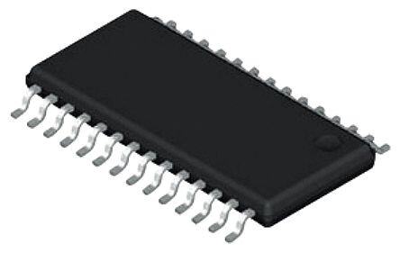
| 供应商器件封装 | 28-TSSOP |
| 其它名称 | 296-33426-5 |
| 制造商产品页 | http://www.ti.com/general/docs/suppproductinfo.tsp?distId=10&orderablePartNumber=MSP430F2132IPW |
| 包装 | 管件 |
| 单位重量 | 117.500 mg |
| 可用A/D通道 | 8 |
| 可编程输入/输出端数量 | 24 |
| 商标 | Texas Instruments |
| 商标名 | MSP430 |
| 处理器系列 | 2 Series |
| 外设 | 欠压检测/复位,POR,PWM,WDT |
| 安装风格 | SMD/SMT |
| 定时器数量 | 2 Timer |
| 封装/外壳 | 28-TSSOP(0.173",4.40mm 宽) |
| 封装/箱体 | TSSOP-28 |
| 工作温度 | -40°C ~ 85°C |
| 工作电源电压 | 1.8 V to 3.6 V |
| 工厂包装数量 | 50 |
| 振荡器类型 | 内部 |
| 接口类型 | USCI (UART, IrDA, LIN, SPI and I2C, SPI) |
| 数据RAM大小 | 512 B |
| 数据总线宽度 | 16 bit |
| 数据转换器 | A/D 8x10b |
| 最大工作温度 | + 85 C |
| 最大时钟频率 | 16 MHz |
| 最小工作温度 | - 40 C |
| 标准包装 | 50 |
| 核心 | MSP430 |
| 核心处理器 | MSP430 |
| 核心尺寸 | 16-位 |
| 片上ADC | Yes |
| 电压-电源(Vcc/Vdd) | 1.8 V ~ 3.6 V |
| 程序存储器大小 | 8 kB |
| 程序存储器类型 | 闪存 |
| 程序存储容量 | 8KB(8K x 8 + 256B) |
| 系列 | MSP430F2132 |
| 输入/输出端数量 | 24 I/O |
| 连接性 | I²C, IrDA, LIN, SCI, SPI, UART/USART |
| 速度 | 16MHz |


- 商务部:美国ITC正式对集成电路等产品启动337调查
- 曝三星4nm工艺存在良率问题 高通将骁龙8 Gen1或转产台积电
- 太阳诱电将投资9.5亿元在常州建新厂生产MLCC 预计2023年完工
- 英特尔发布欧洲新工厂建设计划 深化IDM 2.0 战略
- 台积电先进制程称霸业界 有大客户加持明年业绩稳了
- 达到5530亿美元!SIA预计今年全球半导体销售额将创下新高
- 英特尔拟将自动驾驶子公司Mobileye上市 估值或超500亿美元
- 三星加码芯片和SET,合并消费电子和移动部门,撤换高东真等 CEO
- 三星电子宣布重大人事变动 还合并消费电子和移动部门
- 海关总署:前11个月进口集成电路产品价值2.52万亿元 增长14.8%


PDF Datasheet 数据手册内容提取
MSP430F21x2 www.ti.com SLAS578J–NOVEMBER2007–REVISEDJANUARY2012 MIXED SIGNAL MICROCONTROLLER FEATURES 1 • LowSupplyVoltageRange:1.8Vto3.6V • UniversalSerialCommunicationInterface 2 • Ultra-LowPowerConsumption – EnhancedUARTSupportingAuto-Baudrate – ActiveMode:250µAat1MHz,2.2V Detection(LIN) – StandbyMode:0.7 µA – IrDAEncoderandDecoder – OffMode(RAMRetention):0.1µA – SynchronousSPI • Ultra-FastWake-UpFromStandbyModein – I2C™ LessThan1µs • BrownoutDetector • 16-BitRISCArchitecture,62.5-nsInstruction • SerialOnboardProgramming,NoExternal CycleTime ProgrammingVoltageNeeded,Programmable • BasicClockModuleConfigurations CodeProtectionbySecurityFuse – InternalFrequenciesupto16MHzWith • BootstrapLoader FourCalibratedFrequenciesto±1% • On-ChipEmulationModule – InternalVery-Low-PowerLow-Frequency • FamilyMembersInclude: Oscillator – MSP430F2132 – 32-kHzCrystal – 8KB+256BFlashMemory – High-Frequency(HF)Crystalupto16MHz – 512BRAM – Resonator – MSP430F2122 – ExternalDigitalClockSource – 4KB+256BFlashMemory – ExternalResistor – 512BRAM • 16-BitTimer0_A3WithThreeCapture/Compare – MSP430F2112 Registers – 2KB+256BFlashMemory • 16-BitTimer1_A2WithTwoCapture/Compare – 256BRAM Registers • Availablein28-PinTSSOP(PW)and32-Pin • On-ChipComparatorforAnalogSignal QFN(RHBorRTV)Packages(SeeTable1) CompareFunctionorSlopeAnalog-to-Digital • ForCompleteModuleDescriptions,Seethe (A/D)Conversion MSP430x2xxFamilyUser'sGuide,Literature • 10-Bit200-kspsA/DConverterWithInternal NumberSLAU144 Reference,Sample-and-Hold,Autoscan,and DataTransferController DESCRIPTION TheTexasInstrumentsMSP430™familyofultra-low-powermicrocontrollersconsistsofseveraldevicesfeaturing different sets of peripherals targeted for various applications. The architecture, combined with five low-power modes,isoptimizedtoachieveextendedbatterylifeinportablemeasurementapplications.Thedevicefeaturesa powerful 16-bit RISC CPU, 16-bit registers, and constant generators that contribute to maximum code efficiency. Thedigitallycontrolledoscillator(DCO)allowswake-upfromlow-powermodestoactivemodeinlessthan1µs. The MSP430F21x2 series is an ultra-low-power microcontroller with two built-in 16-bit timers, a fast 10-bit A/D converter with integrated reference and a data transfer controller (DTC), a comparator, built-in communication capabilityusingtheuniversalserialcommunicationinterface,andupto24I/Opins. 1 Pleasebeawarethatanimportantnoticeconcerningavailability,standardwarranty,anduseincriticalapplicationsofTexas Instrumentssemiconductorproductsanddisclaimerstheretoappearsattheendofthisdatasheet. MSP430isatrademarkofTexasInstruments. 2 PRODUCTIONDATAinformationiscurrentasofpublicationdate. Copyright©2007–2012,TexasInstrumentsIncorporated Products conform to specifications per the terms of the Texas Instruments standard warranty. Production processing does not necessarilyincludetestingofallparameters.
MSP430F21x2 SLAS578J–NOVEMBER2007–REVISEDJANUARY2012 www.ti.com This integrated circuit can be damaged by ESD. Texas Instruments recommends that all integrated circuits be handled with appropriateprecautions.Failuretoobserveproperhandlingandinstallationprocedurescancausedamage. ESDdamagecanrangefromsubtleperformancedegradationtocompletedevicefailure.Precisionintegratedcircuitsmaybemore susceptibletodamagebecauseverysmallparametricchangescouldcausethedevicenottomeetitspublishedspecifications. Table1.AvailableOptions PACKAGEDDEVICES(1)(2) T A PLASTIC28-PINTSSOP(PW) PLASTIC32-PINQFN(RHB) PLASTIC32-PINQFN(RTV) MSP430F2112IPW MSP430F2112IRHB MSP430F2112IRTV -40°Cto85°C MSP430F2122IPW MSP430F2122IRHB MSP430F2122IRTV MSP430F2132IPW MSP430F2132IRHB MSP430F2132IRTV MSP430F2112TPW MSP430F2112TRHB MSP430F2112TRTV -40°Cto105°C MSP430F2122TPW MSP430F2122TRHB MSP430F2122TRTV MSP430F2132TPW MSP430F2132TRHB MSP430F2132TRTV (1) Forthemostcurrentpackageandorderinginformation,seethePackageOptionAddendumattheendofthisdocument,orseetheTI websiteatwww.ti.com. (2) Packagedrawings,thermaldata,andsymbolizationareavailableatwww.ti.com/packaging. Development Tool Support All MSP430 microcontrollers include an Embedded Emulation Module (EEM) that allows advanced debugging andprogrammingthrougheasy-to-usedevelopmenttools.Recommendedhardwareoptionsinclude: • DebuggingandProgrammingInterface – MSP-FET430UIF(USB) – MSP-FET430PIF(ParallelPort) • DebuggingandProgrammingInterfacewithTargetBoard – MSP-FET430U28(PWpackage) • ProductionProgrammer – MSP-GANG430 2 SubmitDocumentationFeedback Copyright©2007–2012,TexasInstrumentsIncorporated
MSP430F21x2 www.ti.com SLAS578J–NOVEMBER2007–REVISEDJANUARY2012 Device Pinout, PW Package TEST/SBWTCK 1 28 P1.7/TA0.2/TDO/TDI DV 2 27 P1.6/TA0.1/TDI/TCLK P2.5/R /CAC5C 3 26 P1.5/TA0.0/TMS OSC DV 4 25 P1.4/SMCLK/TCK SS XOUT/P2.7/CA7 5 24 P1.3/TA0.2 XIN/P2.6/CA6 6 23 P1.2/TA0.1 RST/NMI/SBWTDIO 7 22 P1.1/TA0.0/TA1.0 P2.0/ACLK/A0/CA2 8 21 P1.0/TACLK/ADC10CLK/CAOUT P2.1/TAINCLK/SMCLK/A1/CA3 9 20 P2.4/TA0.2/A4/V /Ve /CA1 REF+ REF+ P2.2/TA0.0/A2/CA4/CAOUT 10 19 P2.3/TA0.1/A3/V /Ve /CA0 REF- REF- P3.0/UCB0STE/UCA0CLK/A5 11 18 P3.7/TA1.1/A7 P3.1/UCB0SIMO/UCB0SDA 12 17 P3.6/TA1.0/A6 P3.2/UCB0SOMI/UCB0SCL 13 16 P3.5/UCA0RXD/UCA0SOMI P3.3/UCB0CLK/UCA0STE 14 15 P3.4/UCA0TXD/UCA0SIMO Device Pinout, RHB or RTV Package K DIL TC K A5 TCKTDO/TDI/TTMSK/TC /COSC SBWA0.2/A0.1/A0.0/MCL 2.5/RCVCCEST/1.7/T1.6/T1.5/T1.4/S PNDTPPPP 32 31 30 29 28 27 26 25 DV 1 24 P1.3/TA0.2 SS XOUT/P2.7/CA7 2 23 P1.2/TA0.1 XIN/P2.6/CA6 3 22 P1.1/TA0.0/TA1.0 NC 4 21 P1.0/TACLK/ADC10CLK/CAOUT RST/NMI/SBWTDIO 5 20 NC P2.0/ACLK/A0/CA2 6 19 P2.4/TA0.2/A4/V /Ve /CA1 REF+ REF+ P2.1/TAINCLK/SMCLK/A1/CA3 7 18 P2.3/TA0.1/A3/V /Ve /CA0 REF- REF- P2.2/TA0.0/A2/CA4/CAOUT 8 17 NC 9 10 11 12 13 14 15 16 B0STE/UCA0CLK/A5CB0SIMO/UCB0SDACB0SOMI/UCB0SCLUCB0CLK/UCA0STECA0TXD/UCA0SIMOCA0RXD/UCA0SOMIP3.6/TA1.0/A6P3.7/TA1.1/A7 0/UC3.1/U3.2/UP3.3/3.4/U3.5/U 3.PP PP P Copyright©2007–2012,TexasInstrumentsIncorporated SubmitDocumentationFeedback 3
MSP430F21x2 SLAS578J–NOVEMBER2007–REVISEDJANUARY2012 www.ti.com Functional Block Diagram XIN XOUT DVCC D/AVSS AVCC P1.x P2.x P3.x 8 8 8 ACLK Basic Clock ADC10 Port P1 Port P2 Port P3 System+ SMCLK Flash RAM 8 I/O 8 I/O 8 I/O 10-bit 8kB 512B Interrupt Interrupt 8 Channels 4kB 512B capability capability pullup/ MCLK 2kB 256B Autoscan pullup/down pullup/down pulldown DTC resistors resistors resistors 16MHz CPU MAB incl. 16 Registers MDB Emulation 2BP USCIA0 Watchdog Timer0_A3 Timer1_A2 UART/LIN, JTAG PBrrootwecntoiount Comp_A+ WDT+ 3 CC 2 CC IrDA, SPI Interface 15-Bit Registers Registers USCI B0 SPI, I2C Spy-Bi Wire RST/NMI 4 SubmitDocumentationFeedback Copyright©2007–2012,TexasInstrumentsIncorporated
MSP430F21x2 www.ti.com SLAS578J–NOVEMBER2007–REVISEDJANUARY2012 Table2.TerminalFunctions TERMINAL NO. I/O DESCRIPTION NAME RHB, PW RTV General-purposedigitalI/Opin Timer0_A3,clocksignalTACLKinput P1.0/TACLK/ADC10CLK/CAOUT 21 21 I/O Timer1_A2,clocksignalTACLKinput ADC10,conversionclock Comparator_A+output General-purposedigitalI/Opin P1.1/TA0.0/TA1.0 22 22 I/O Timer0_A3,capture:CCI0Ainput,compare:Out0Output Timer1_A2,capture:CCI0Ainput General-purposedigitalI/Opin P1.2/TA0.1 23 23 I/O Timer0_A3,capture:CCI1Ainput,compare:Out1Output General-purposedigitalI/Opin P1.3/TA0.2 24 24 I/O Timer0_A3,capture:CCI2Ainput,compare:Out2Output General-purposedigitalI/Opin P1.4/SMCLK/TCK 25 25 I/O SMCLKsignaloutput TestClockinputfordeviceprogrammingandtest General-purposedigitalI/Opin P1.5/TA0.0/TMS 26 26 I/O Timer0_A3,compare:Out0Output JTAGtestmodeselect,inputterminalfordeviceprogrammingandtest General-purposedigitalI/Opin P1.6/TA0.1/TDI/TCLK 27 27 I/O Timer0_A3,compare:Out1Output JTAGtestdatainputortestclockinputinprogrammingantest General-purposedigitalI/Opin P1.7/TA0.2/TDO/TDI 28 28 I/O Timer0_A3,compare:Out2Output JTAGtestdataoutputterminalortestdatainputinprogrammingantest General-purposedigitalI/Opin ACLKsignaloutput P2.0/ACLK/A0/CA2 8 6 I/O ADC10analoginputA0 Comparator_A+input General-purposedigitalI/Opin SMCLKsignaloutput Timer0_A3,clocksignalTACLKinput P2.1/TAINCLK/SMCLK/A1/CA3 9 7 I/O Timer1_A2,clocksignalTACLKinput ADC10analoginputA1 Comparator_A+input General-purposedigitalI/Opin Timer0_A3,capture:CCI0Binput,compare:Out0Output P2.2/TA0.0/A2/CA4/CAOUT 10 8 I/O ADC10analoginputA2 Comparator_A+input Comparator_A+output General-purposedigitalI/Opin Timer0_A3,compare:Out1Output P2.3/TA0.1/A3/V /Ve /CA0 19 18 I/O REF- REF- ADC10analoginputA3/negativereference Comparator_A+input Copyright©2007–2012,TexasInstrumentsIncorporated SubmitDocumentationFeedback 5
MSP430F21x2 SLAS578J–NOVEMBER2007–REVISEDJANUARY2012 www.ti.com Table2.TerminalFunctions(continued) TERMINAL NO. I/O DESCRIPTION NAME RHB, PW RTV General-purposedigitalI/Opin Timer0_A3,compare:Out2Output P2.4/TA0.2/A4/V /Ve /CA1 20 19 I/O REF+ REF+ ADC10analoginputA4/positivereference Comparator_A+input Inputterminalofcrystaloscillator XIN/P2.6/CA6 6 3 I/O General-purposedigitalI/Opin Comparator_A+input Outputterminalofcrystaloscillator XOUT/P2.7/CA7 5 2 I/O General-purposedigitalI/Opin Comparator_A+input General-purposedigitalI/Opin P3.0/UCB0STE/UCA0CLK/A5 11 9 I/O USCI_B0slavetransmitenable/USCI_A0clockinput/output ADC10analoginputA5 General-purposedigitalI/Opin P3.1/UCB0SIMO/UCB0SDA 12 10 I/O USCI_B0slavein/masteroutinSPImode,SDAI2CdatainI2Cmode General-purposedigitalI/Opin P3.2/UCB0SOMI/UCB0SCL 13 11 I/O USCI_B0slaveout/masterininSPImode,SCLI2CclockinI2Cmode General-purposedigitalI/O P3.3/UCB0CLK/UCA0STE 14 12 I/O USCI_B0clockinput/output,USCI_A0slavetransmitenable General-purposedigitalI/Opin P3.4/UCA0TXD/UCA0SIMO 15 13 I/O USCI_A0transmitdataoutputinUARTmode,slavedatain/masterout inSPImode General-purposedigitalI/Opin P3.5/UCA0RXD/UCA0SOMI 16 14 I/O USCI_A0receivedatainputinUARTmode,slavedataout/masterinin SPImode General-purposedigitalI/Opin P3.6/TA1.0/A6 17 15 I/O Timer1_A2,capture:CCI0Binput,compare:Out0Output ADC10analoginputA6 General-purposedigitalI/Opin P3.7/TA1.1/A7 18 16 I/O Timer1_A2,capture:CCI1Ainput,compare:Out1Output ADC10analoginputA7 Resetornonmaskableinterruptinput RST/NMI/SBWTDIO 7 5 I Spy-Bi-Wiretestdatainput/outputduringprogrammingandtest SelectstestmodeforJTAGpinsonPort1.Thedeviceprotectionfuseis TEST/SBWTCK 1 29 I connectedtoTEST. General-purposedigitalI/Opin P2.5/R /CA5 3 32 I/O InputforexternalresistordefiningtheDCOnominalfrequency OSC Comparator_A+input DV 2 30 Digitalsupplyvoltage CC DV 4 1 Digitalsupplyvoltage SS 4,17,20, NC NA Notconnectedinternally.ConnectiontoV isrecommended. 31 SS QFNpackagepad(RHB,RTVpackages).ConnectiontoDV is QFNPad NA Pad SS recommended. 6 SubmitDocumentationFeedback Copyright©2007–2012,TexasInstrumentsIncorporated
MSP430F21x2 www.ti.com SLAS578J–NOVEMBER2007–REVISEDJANUARY2012 SHORT-FORM DESCRIPTION CPU Program Counter PC/R0 The MSP430™ CPU has a 16-bit RISC architecture Stack Pointer SP/R1 that is highly transparent to the application. All operations, other than program-flow instructions, are Status Register SR/CG1/R2 performed as register operations in conjunction with seven addressing modes for source operand and four Constant Generator CG2/R3 addressingmodesfordestinationoperand. General-Purpose Register R4 The CPU is integrated with 16 registers that provide reduced instruction execution time. The General-Purpose Register R5 register-to-register operation execution time is one cycleoftheCPUclock. General-Purpose Register R6 Four of the registers, R0 to R3, are dedicated as program counter, stack pointer, status register, and General-Purpose Register R7 constant generator respectively. The remaining registersaregeneral-purposeregisters. General-Purpose Register R8 Peripherals are connected to the CPU using data, General-Purpose Register R9 address, and control buses and can be handled with allinstructions. General-Purpose Register R10 Instruction Set General-Purpose Register R11 The instruction set consists of 51 instructions with General-Purpose Register R12 three formats and seven address modes. Each instruction can operate on word and byte data. General-Purpose Register R13 Table 3 shows examples of the three types of instruction formats; Table 4 shows the address General-Purpose Register R14 modes. General-Purpose Register R15 Table3.InstructionWordFormats INSTRUCTIONFORMAT EXAMPLE OPERATION Dualoperands,source-destination ADDR4,R5 R4+R5→R5 Singleoperands,destinationonly CALLR8 PC→(TOS),R8→PC Relativejump,unconditional/conditional JNE Jump-on-equalbit=0 Table4.AddressModeDescriptions ADDRESSMODE S(1) D(2) SYNTAX EXAMPLE OPERATION Register ✓ ✓ MOVRs,Rd MOVR10,R11 R10→R11 Indexed ✓ ✓ MOVX(Rn),Y(Rm) MOV2(R5),6(R6) M(2+R5)→M(6+R6) Symbolic(PCrelative) ✓ ✓ MOVEDE,TONI M(EDE)→M(TONI) Absolute ✓ ✓ MOV&MEM,&TCDAT M(MEM)→M(TCDAT) Indirect ✓ MOV@Rn,Y(Rm) MOV@R10,Tab(R6) M(R10)→M(Tab+R6) M(R10)→R11 Indirectautoincrement ✓ MOV@Rn+,Rm MOV@R10+,R11 R10+2→R10 Immediate ✓ MOV#X,TONI MOV#45,TONI #45→M(TONI) (1) S=source (2) D=destination Copyright©2007–2012,TexasInstrumentsIncorporated SubmitDocumentationFeedback 7
MSP430F21x2 SLAS578J–NOVEMBER2007–REVISEDJANUARY2012 www.ti.com Operating Modes The MSP430 microcontrollers have one active mode and five software-selectable low-power modes of operation. An interrupt event can wake up the device from any of the five low-power modes, service the request, and restorebacktothelow-powermodeonreturnfromtheinterruptprogram. Thefollowingsixoperatingmodescanbeconfiguredbysoftware: • Activemode(AM) – Allclocksareactive. • Low-powermode0(LPM0) – CPUisdisabled. – ACLKandSMCLKremainactive.MCLKisdisabled. • Low-powermode1(LPM1) – CPUisdisabledACLKandSMCLKremainactive.MCLKisdisabled. – DCOdc-generatorisdisabledifDCOnotusedinactivemode. • Low-powermode2(LPM2) – CPUisdisabled. – MCLKandSMCLKaredisabled. – DCOdc-generatorremainsenabled. – ACLKremainsactive. • Low-powermode3(LPM3) – CPUisdisabled. – MCLKandSMCLKaredisabled. – DCOdc-generatorisdisabled. – ACLKremainsactive. • Low-powermode4(LPM4) – CPUisdisabled. – ACLKisdisabled. – MCLKandSMCLKaredisabled. – DCOdc-generatorisdisabled. – Crystaloscillatorisstopped. 8 SubmitDocumentationFeedback Copyright©2007–2012,TexasInstrumentsIncorporated
MSP430F21x2 www.ti.com SLAS578J–NOVEMBER2007–REVISEDJANUARY2012 Interrupt Vector Addresses The interrupt vectors and the power-up starting address are located in the address range of 0xFFFF to 0xFFC0. Thevectorcontainsthe16-bitaddressoftheappropriateinterrupthandlerinstructionsequence. If the reset vector (located at address 0xFFFE) contains 0xFFFF (for example, if flash is not programmed), the CPUgoesintoLPM4immediatelyafterpowerup. Table5.InterruptVectorAddresses INTERRUPTSOURCE INTERRUPTFLAG SYSTEMINTERRUPT WORDADDRESS PRIORITY Power-up PORIFG Externalreset RSTIFG Watchdog WDTIFG Reset 0xFFFE 31,highest Flashkeyviolation KEYV(1) PCoutofrange(2) NMI NMIIFG (Non)maskable Oscillatorfault OFIFG (Non)maskable 0xFFFC 30 Flashmemoryaccessviolation ACCVIFG(1)(3) (Non)maskable Timer1_A2 TA1CCR0CCIFG(4) Maskable 0xFFFA 29 TA1CCR1CCIFG, Timer1_A2 Maskable 0xFFF8 28 TA1CTLTAIFG(1)(4) Comparator_A+ CAIFG Maskable 0xFFF6 27 Watchdogtimer WDTIFG Maskable 0xFFF4 26 Timer0_A3 TA0CCR0CCIFG(4) Maskable 0xFFF2 25 TA0CCR1CCIFG, Timer0_A3 TA0CCR2CCIFG, Maskable 0xFFF0 24 TA0CTLTAIFG(1)(4) USCI_A0/USCI_B0receive UCA0RXIFG, USCI_B0I2Cstatus UCB0RXIFG(1)(5) Maskable 0xFFEE 23 USCI_A0/USCI_B0transmit UCA0TXIFG, USCI_B0I2Creceive/transmit UCB0TXIFG(1)(6) Maskable 0xFFEC 22 ADC10 ADC10IFG(4) Maskable 0xFFEA 21 0xFFE8 20 I/OportP2(eightflags) P2IFG.0toP2IFG.7(1)(4) Maskable 0xFFE6 19 I/OportP1(eightflags) P1IFG.0toP1IFG.7(1)(4) Maskable 0xFFE4 18 0xFFE2 17 0xFFE0 16 See (7) 0xFFDE 15 See (8) 0xFFDCto0xFFC0 14to0,lowest (1) Multiplesourceflags (2) AresetisgeneratediftheCPUtriestofetchinstructionsfromwithinthemoduleregistermemoryaddressrange(0x0000to0x01FF)or fromwithinunusedaddressrange. (3) (non)-maskable:theindividualinterrupt-enablebitcandisableaninterruptevent,butthegeneralinterruptenablecannot. Nonmaskable:neithertheindividualnorthegeneralinterrupt-enablebitwilldisableaninterruptevent. (4) Interruptflagsarelocatedinthemodule. (5) InSPImode:UCB0RXIFG.InI2Cmode:UCALIFG,UCNACKIFG,ICSTTIFG,UCSTPIFG (6) InUART/SPImode:UCB0TXIFG.InI2Cmode:UCB0RXIFG,UCB0TXIFG (7) Thislocationisusedasbootstraploadersecuritykey(BSLSKEY). A0xAA55atthislocationdisablestheBSLcompletely. Azero(0x0)disablestheerasureoftheflashifaninvalidpasswordissupplied. (8) Theinterruptvectorsataddresses0xFFDCto0xFFC0arenotusedinthisdeviceandcanbeusedforregularprogramcodeif necessary. Copyright©2007–2012,TexasInstrumentsIncorporated SubmitDocumentationFeedback 9
MSP430F21x2 SLAS578J–NOVEMBER2007–REVISEDJANUARY2012 www.ti.com Special Function Registers Most interrupt and module enable bits are collected into the lowest address space. Special function register bits not allocated to a functional purpose are not physically present in the device. Simple software access is provided withthisarrangement. Legend rw Bitcanbereadandwritten. rw-0,1 Bitcanbereadandwritten.ItisResetorSetbyPUC. rw-(0),(1) Bitcanbereadandwritten.ItisResetorSetbyPOR. SFRbitisnotpresentindevice. Table6.InterruptEnable1 Address 7 6 5 4 3 2 1 0 00h ACCVIE NMIIE OFIE WDTIE rw-0 rw-0 rw-0 rw-0 WDTIE Watchdogtimerinterruptenable.Inactiveifwatchdogmodeisselected.Activeifwatchdogtimerisconfiguredininterval timermode. OFIE Oscillatorfaultinterruptenable NMIIE (Non)maskableinterruptenable ACCVIE Flashaccessviolationinterruptenable Table7.InterruptEnable2 Address 7 6 5 4 3 2 1 0 01h UCB0TXIE UCB0RXIE UCA0TXIE UCA0RXIE rw-0 rw-0 rw-0 rw-0 UCA0RXIE USCI_A0receive-interruptenable UCA0TXIE USCI_A0transmit-interruptenable UCB0RXIE USCI_B0receive-interruptenable UCB0TXIE USCI_B0transmit-interruptenable Table8.InterruptFlagRegister1 Address 7 6 5 4 3 2 1 0 02h NMIIFG RSTIFG PORIFG OFIFG WDTIFG rw-0 rw-(0) rw-(1) rw-1 rw-(0) WDTIFG Setonwatchdogtimeroverflow(inwatchdogmode)orsecuritykeyviolation. ResetonV power-uporaresetconditionatRST/NMIpininresetmode. CC OFIFG Flagsetonoscillatorfault RSTIFG Externalresetinterruptflag.SetonaresetconditionatRST/NMIpininresetmode.ResetonV powerup. CC PORIFG Power-onresetinterruptflag.SetonV powerup. CC NMIIFG SetviaRST/NMIpin Table9.InterruptFlagRegister2 Address 7 6 5 4 3 2 1 0 03h UCB0TXIFG UCB0RXIFG UCA0TXIFG UCA0RXIFG rw-1 rw-0 rw-1 rw-0 UCA0RXIFG USCI_A0receive-interruptflag UCA0TXIFG USCI_A0transmit-interruptflag UCB0RXIFG USCI_B0receive-interruptflag UCB0TXIFG USCI_B0transmit-interruptflag 10 SubmitDocumentationFeedback Copyright©2007–2012,TexasInstrumentsIncorporated
MSP430F21x2 www.ti.com SLAS578J–NOVEMBER2007–REVISEDJANUARY2012 Memory Organization Table10.MemoryOrganization MSP430F2112 MSP430F2122 MSP430F2132 Memory Size 2KB 4KB 8KB Main:interruptvector Flash 0xFFFFto0xFFC0 0xFFFFto0xFFC0 0xFFFFto0xFFC0 Main:codememory Flash 0xFFFFto0xF800 0xFFFFto0xF000 0xFFFFto0xE000 Informationmemory Size 256Byte 256Byte 256Byte Flash 0x10FFhto0x1000 0x10FFhto0x1000 0x10FFhto0x1000 Bootmemory Size 1KB 1KB 1KB ROM 0x0FFFto0x0C00 0x0FFFto0x0C00 0x0FFFto0x0C00 RAM Size 256B 512Byte 512Byte 0x02FFto0x0200 0x03FFto0x0200 0x03FFto0x0200 Peripherals 16-bit 0x01FFto0x0100 0x01FFto0x0100 0x01FFto0x0100 8-bit 0x00FFto0x0010 0x00FFto0x0010 0x00FFto0x0010 8-bitSFR 0x000Fto0x0000 0x000Fto0x0000 0x000Fto0x0000 Bootstrap Loader (BSL) The MSP430 bootstrap loader (BSL) enables users to program the flash memory or RAM using a UART serial interface. Access to the MSP430 memory via the BSL is protected by user-defined password. For complete description of the features of the BSL and its implementation, see the MSP430 Programming Via the Bootstrap LoaderUser’sGuide,literaturenumberSLAU319. Table11.BSLFunctionPins BSLFUNCTION PWPACKAGEPINS RHB,RTVPACKAGEPINS Datatransmit 22-P1.1 22-P1.1 Datareceive 10-P2.2 8-P2.2 Flash Memory The flash memory can be programmed via the JTAG port, the bootstrap loader, or in-system by the CPU. The CPUcanperformsingle-byteandsingle-wordwritestotheflashmemory.Featuresoftheflashmemoryinclude: • Flash memory has n segments of main memory and four segments of information memory (A to D) of 64byteseach.Eachsegmentinmainmemoryis512bytesinsize. • Segments0tonmaybeerasedinonestep,oreachsegmentmaybeindividuallyerased. • SegmentsAtoDcanbeerasedindividually,orasagroupwithsegments0ton. SegmentsAtoDarealsocalledinformationmemory. • Segment A contains calibration data. After reset, segment A is protected against programming and erasing. It can be unlocked, but care should be taken not to erase this segment if the device-specific calibration data is required. Copyright©2007–2012,TexasInstrumentsIncorporated SubmitDocumentationFeedback 11
MSP430F21x2 SLAS578J–NOVEMBER2007–REVISEDJANUARY2012 www.ti.com Peripherals Peripherals are connected to the CPU through data, address, and control buses and can be handled using all instructions.Forcompletemoduledescriptions,seetheMSP430x2xxFamilyUser'sGuide(SLAU144). Oscillator and System Clock The clock system is supported by the basic clock module that includes support for a 32768-Hz watch crystal oscillator,aninternalvery-low-powerlow-frequencyoscillator,aninternaldigitally-controlledoscillator(DCO),and a high-frequency crystal oscillator. The basic clock module is designed to meet the requirements of both low system cost and low power consumption. The internal DCO provides a fast turn-on clock source and stabilizes in lessthan1µs.Thebasicclockmoduleprovidesthefollowingclocksignals: • Auxiliary clock (ACLK), sourced from a 32768-Hz watch crystal, a high-frequency crystal, or the internal very-low-powerLFoscillator. • Mainclock(MCLK),thesystemclockusedbytheCPU. • Sub-Mainclock(SMCLK),thesub-systemclockusedbytheperipheralmodules. TheDCOsettingstocalibratetheDCOoutputfrequencyarestoredintheinformationmemorysegmentA. Calibration Data Stored in Information Memory Segment A CalibrationdataisstoredforboththeDCOandforADC10organizedinatag-length-value(TLV)structure. Table12.TagsUsedbytheADCCalibrationTags NAME ADDRESS VALUE DESCRIPTION TAG_DCO_30 0x10F6 0x01 DCOfrequencycalibrationatV =3VandT =30°Catcalibration CC A TAG_ADC10_1 0x10DA 0x08 ADC10_1calibrationtag TAG_EMPTY - 0xFE Identifierforemptymemoryareas Table13.LabelsUsedbytheADCCalibrationTags ADDRESS LABEL CONDITIONATCALIBRATION/DESCRIPTION SIZE OFFSET CAL_ADC_25T85 INCHx=0x1010,REF2_5=1,T =85°C word 0x0010 A CAL_ADC_25T30 INCHx=0x1010,REF2_5=1,T =30°C word 0x000E A CAL_ADC_25VREF_FACTOR REF2_5=1,T =30°C,I =1mA word 0x000C A VREF+ CAL_ADC_15T85 INCHx=0x1010,REF2_5=0,T =85°C word 0x000A A CAL_ADC_15T30 INCHx=0x1010,REF2_5=0,T =30°C word 0x0008 A CAL_ADC_15VREF_FACTOR REF2_5=0,T =30°C,I =0.5mA word 0x0006 A VREF+ CAL_ADC_OFFSET ExternalV =1.5V,f =5MHz word 0x0004 REF ADC10CLK CAL_ADC_GAIN_FACTOR ExternalV =1.5V,f =5MHz word 0x0002 REF ADC10CLK CAL_BC1_1MHz - byte 0x0009 CAL_DCO_1MHz - byte 0x0008 CAL_BC1_8MHz - byte 0x0007 CAL_DCO_8MHz - byte 0x0006 CAL_BC1_12MHz - byte 0x0005 CAL_DCO_12MHz - byte 0x0004 CAL_BC1_16MHz - byte 0x0003 CAL_DCO_16MHz - byte 0x0002 12 SubmitDocumentationFeedback Copyright©2007–2012,TexasInstrumentsIncorporated
MSP430F21x2 www.ti.com SLAS578J–NOVEMBER2007–REVISEDJANUARY2012 Brownout The brownout circuit is implemented to provide the proper internal reset signal to the device during power on and poweroff. Digital I/O Therearethree8-bitI/Oportsimplemented—portsP1,P2,andP3: • AllindividualI/Obitsareindependentlyprogrammable. • Anycombinationofinput,output,andinterruptconditionispossible. • Edge-selectableinterruptinputcapabilityforalleightbitsofportP1andP2. • Read/writeaccesstoport-controlregistersissupportedbyallinstructions. • EachI/Ohasanindividuallyprogrammablepullup/pulldownresistor. The MSP430F21x2 devices provide up to 24 total port I/O pins available externally. See the device pinout for moreinformation. Watchdog Timer (WDT+) The primary function of the WDT+ module is to perform a controlled system restart after a software problem occurs. If the selected time interval expires, a system reset is generated. If the watchdog function is not needed in an application, the module can be disabled or configured as an interval timer and can generate interrupts at selectedtimeintervals. ADC10 The ADC10 module supports fast, 10-bit analog-to-digital conversions. The module implements a 10-bit SAR core, sample select control, reference generator and data transfer controller, or DTC, for automatic conversion resulthandlingallowingADCsamplestobeconvertedandstoredwithoutanyCPUintervention. Comparator_A+ The primary function of the comparator_A+ module is to support precision slope analog-to-digital conversions, battery-voltagesupervision,andmonitoringofexternalanalogsignals. Copyright©2007–2012,TexasInstrumentsIncorporated SubmitDocumentationFeedback 13
MSP430F21x2 SLAS578J–NOVEMBER2007–REVISEDJANUARY2012 www.ti.com Timer0_A3 Timer0_A3 is a 16-bit timer/counter with three capture/compare registers. Timer0_A3 can support multiple capture/compares, PWM outputs, and interval timing. Timer0_A3 also has extensive interrupt capabilities. Interrupts may be generated from the counter on overflow conditions and from each of the capture/compare registers. Table14.Timer0_A3SignalConnections INPUTPINNUMBER MODULE OUTPUTPINNUMBER DEVICEINPUT MODULE MODULE OUTPUT PW RHB,RTV SIGNAL INPUTNAME BLOCK SIGNAL PW RHB,RTV 21-P1.0 21-P1.0 TACLK TACLK Timer NA ACLK ACLK SMCLK SMCLK 9-P2.1 7-P2.1 TAINCLK INCLK 22-P1.1 22-P1.1 TA0 CCI0A CCR0 TA0 22-P1.1 22-P1.1 10-P2.2 8-P2.2 TA0 CCI0B 26-P1.5 26-P1.5 DV GND 10-P2.2 8-P2.2 SS ADC10 ADC10 DV V CC CC (internal) (internal) 23-P1.2 23-P1.2 TA1 CCI1A CCR1 TA1 23-P1.2 23-P1.2 CAOUT CCI1B 27-P1.6 27-P1.6 (internal) DV GND 19-P2.3 18-P2.3 SS ADC10 ADC10 DV V CC CC (internal) (internal) 24-P1.3 24-P1.3 TA2 CCI2A CCR2 TA2 24-P1.3 24-P1.3 ACLK(internal) CCI2B 28-P1.7 28-P1.7 DV GND 20-P2.4 19-P2.4 SS ADC10 ADC10 DV V CC CC (internal) (internal) 14 SubmitDocumentationFeedback Copyright©2007–2012,TexasInstrumentsIncorporated
MSP430F21x2 www.ti.com SLAS578J–NOVEMBER2007–REVISEDJANUARY2012 Timer1_A2 Timer1_A2 is a 16-bit timer/counter with two capture/compare registers. Timer1_A2 can support multiple capture/compares, PWM outputs, and interval timing. Timer1_A2 also has extensive interrupt capabilities. Interrupts may be generated from the counter on overflow conditions and from each of the capture/compare registers. Table15.Timer1_A2SignalConnections INPUTPINNUMBER MODULE OUTPUTPINNUMBER DEVICEINPUT MODULE MODULE OUTPUT PW RHB,RTV SIGNAL INPUTNAME BLOCK SIGNAL PW RHB,RTV 21-P1.0 21-P1.0 TACLK TACLK Timer NA ACLK ACLK SMCLK SMCLK 9-P2.1 7-P2.1 TAINCLK INCLK 22-P1.1 22-P1.1 TA0 CCI0A CCR0 TA0 17-P3.6 15-P3.6 17-P3.6 15-P3.6 TA0 CCI0B DV GND SS DV V CC CC 18-P3.7 16-P3.7 TA1 CCI1A CCR1 TA1 18-P3.7 16-P3.7 CAOUT CCI1B (internal) DV GND SS DV V CC CC Universal Serial Communications Interface (USCI) The USCI module is used for serial data communication. The USCI module supports synchronous communication protocols like SPI (3 or 4 pin), I2C and asynchronous communication protocols such as UART, enhancedUARTwithautomaticbaudratedetection(LIN),andIrDA. USCI_A0providessupportforSPI(3or4pin),UART,enhancedUART,andIrDA. USCI_B0providessupportforSPI(3or4pin)andI2C. Copyright©2007–2012,TexasInstrumentsIncorporated SubmitDocumentationFeedback 15
MSP430F21x2 SLAS578J–NOVEMBER2007–REVISEDJANUARY2012 www.ti.com Peripheral File Map Table16.PeripheralsWithWordAccess MODULE REGISTERNAME SHORTNAME ADDRESSOFFSET ADC10 ADCdatatransferstartaddress ADC10SA 0x01BC ADCmemory ADC10MEM 0x01B4 ADCcontrolregister1 ADC10CTL1 0x01B2 ADCcontrolregister0 ADC10CTL0 0x01B0 ADCanalogenable0 ADC10AE0 0x004A ADCanalogenable1 ADC10AE1 0x004B ADCdatatransfercontrolregister1 ADC10DTC1 0x0049 ADCdatatransfercontrolregister0 ADC10DTC0 0x0048 Timer0_A3 Capture/compareregister TA0CCR2 0x0176 Capture/compareregister TA0CCR1 0x0174 Capture/compareregister TA0CCR0 0x0172 Timer0_A3register TA0R 0x0170 Capture/comparecontrol TA0CCTL2 0x0166 Capture/comparecontrol TA0CCTL1 0x0164 Capture/comparecontrol TA0CCTL0 0x0162 Timer0_A3control TA0CTL 0x0160 Timer0_A3interruptvector TA0IV 0x012E Timer1_A2 Capture/compareregister TA1CCR1 0x0194 Capture/compareregister TA1CCR0 0x0192 Timer1_A2register TA1R 0x0190 Capture/comparecontrol TA1CCTL1 0x0184 Capture/comparecontrol TA1CCTL0 0x0182 Timer1_A2control TA1CTL 0x0180 Timer1_A2interruptvector TA1IV 0x011E FlashMemory Flashcontrol3 FCTL3 0x012C Flashcontrol2 FCTL2 0x012A Flashcontrol1 FCTL1 0x0128 WatchdogTimer+ Watchdog/timercontrol WDTCTL 0x0120 Table17.PeripheralsWithByteAccess MODULE REGISTERNAME SHORTNAME ADDRESSOFFSET USCI_B0 USCI_B0transmitbuffer UCB0TXBUF 0x06F USCI_B0receivebuffer UCB0RXBUF 0x06E USCI_B0status UCB0STAT 0x06D USCIB0I2CInterruptenable UCB0CIE 0x06C USCI_B0bitratecontrol1 UCB0BR1 0x06B USCI_B0bitratecontrol0 UCB0BR0 0x06A USCI_B0control1 UCB0CTL1 0x069 USCI_B0control0 UCB0CTL0 0x068 USCI_B0I2Cslaveaddress UCB0SA 0x011A USCI_B0I2Cownaddress UCB0OA 0x0118 16 SubmitDocumentationFeedback Copyright©2007–2012,TexasInstrumentsIncorporated
MSP430F21x2 www.ti.com SLAS578J–NOVEMBER2007–REVISEDJANUARY2012 Table17.PeripheralsWithByteAccess(continued) MODULE REGISTERNAME SHORTNAME ADDRESSOFFSET USCI_A0 USCI_A0transmitbuffer UCA0TXBUF 0x0067 USCI_A0receivebuffer UCA0RXBUF 0x0066 USCI_A0status UCA0STAT 0x0065 USCI_A0modulationcontrol UCA0MCTL 0x0064 USCI_A0baudratecontrol1 UCA0BR1 0x0063 USCI_A0baudratecontrol0 UCA0BR0 0x0062 USCI_A0control1 UCA0CTL1 0x0061 USCI_A0control0 UCA0CTL0 0x0060 USCI_A0IrDAreceivecontrol UCA0IRRCTL 0x005F USCI_A0IrDAtransmitcontrol UCA0IRTCTL 0x005E USCI_A0autobaudratecontrol UCA0ABCTL 0x005D Comparator_A+ Comparator_Aportdisable CAPD 0x005B Comparator_Acontrol2 CACTL2 0x005A Comparator_Acontrol1 CACTL1 0x0059 BasicClockSystem+ Basicclocksystemcontrol3 BCSCTL3 0x0053 Basicclocksystemcontrol2 BCSCTL2 0x0058 Basicclocksystemcontrol1 BCSCTL1 0x0057 DCOclockfrequencycontrol DCOCTL 0x0056 PortP3 PortP3resistorenable P3REN 0x0010 PortP3selection P3SEL 0x001B PortP3direction P3DIR 0x001A PortP3output P3OUT 0x0019 PortP3input P3IN 0x0018 PortP2 PortP2selection2 P2SEL2 0x0042 PortP2resistorenable P2REN 0x002F PortP2selection P2SEL 0x002E PortP2interruptenable P2IE 0x002D PortP2interruptedgeselect P2IES 0x002C PortP2interruptflag P2IFG 0x002B PortP2direction P2DIR 0x002A PortP2output P2OUT 0x0029 PortP2input P2IN 0x0028 PortP1 PortP1selection2register P1SEL2 0x0041 PortP1resistorenable P1REN 0x0027 PortP1selection P1SEL 0x0026 PortP1interruptenable P1IE 0x0025 PortP1interruptedgeselect P1IES 0x0024 PortP1interruptflag P1IFG 0x0023 PortP1direction P1DIR 0x0022 PortP1output P1OUT 0x0021 PortP1input P1IN 0x0020 SpecialFunction SFRinterruptflag2 IFG2 0x0003 SFRinterruptflag1 IFG1 0x0002 SFRinterruptenable2 IE2 0x0001 SFRinterruptenable1 IE1 0x0000 Copyright©2007–2012,TexasInstrumentsIncorporated SubmitDocumentationFeedback 17
MSP430F21x2 SLAS578J–NOVEMBER2007–REVISEDJANUARY2012 www.ti.com Absolute Maximum Ratings(1) VoltageappliedatV toV -0.3Vto4.1V CC SS Voltageappliedtoanypin (2) -0.3VtoV +0.3V CC Diodecurrentatanydeviceterminal ±2mA Unprogrammeddevice -55°Cto150°C Storagetemperature,T (3) stg Programmeddevice -55°Cto150°C (1) Stressesbeyondthoselistedunderabsolutemaximumratingsmaycausepermanentdamagetothedevice.Thesearestressratings only,andfunctionaloperationofthedeviceattheseoranyotherconditionsbeyondthoseindicatedunderrecommendedoperating conditionsisnotimplied.Exposuretoabsolute-maximum-ratedconditionsforextendedperiodsmayaffectdevicereliability. (2) AllvoltagesreferencedtoV .TheJTAGfuse-blowvoltage,V ,isallowedtoexceedtheabsolutemaximumrating.Thevoltageis SS FB appliedtotheTESTpinwhenblowingtheJTAGfuse. (3) HighertemperaturemaybeappliedduringboardsolderingprocessaccordingtothecurrentJEDECJ-STD-020specificationwithpeak reflowtemperaturesnothigherthanclassifiedonthedevicelabelontheshippingboxesorreels. Recommended Operating Conditions(1) MIN NOM MAX UNIT Duringprogramexecution 1.8 3.6 V Supplyvoltage,AV =DV =V V CC CC CC CC Duringflashmemoryprogramming 2.2 3.6 V Supplyvoltage AV =DV =V 0 0 V SS SS SS SS Iversion -40 85 T Operatingfree-airtemperature °C A Tversion -40 105 V =1.8V,Dutycycle=50%±10% dc 6 Processorfrequency(maximumMCLK CC f frequency)(2)(1) V =2.7V,Dutycycle=50%±10% dc 12 MHz SYSTEM CC (seeFigure1) V ≥3.3V,Dutycycle=50%±10% dc 16 CC (1) Modulesmighthaveadifferentmaximuminputclockspecification.Seethespecificationoftherespectivemoduleinthisdatasheet. (2) TheMSP430CPUisclockeddirectlywithMCLK.BoththehighandlowphaseofMCLKmustnotexceedthepulsewidthofthe specifiedmaximumfrequency. Legend: 16MHz Supply voltage range during flash memory z H programming M − 12MHz y c n e Supply voltage range u q during program execution e Fr m e 6MHz st y S 1.8V 2.2V 2.7V 3.3V 3.6V Supply Voltage−V NOTE: Minimumprocessorfrequencyisdefinedbysystemclock.FlashprogramoreraseoperationsrequireaminimumV CC of2.2V. Figure1. OperatingArea 18 SubmitDocumentationFeedback Copyright©2007–2012,TexasInstrumentsIncorporated
MSP430F21x2 www.ti.com SLAS578J–NOVEMBER2007–REVISEDJANUARY2012 Active Mode Supply Current (into DV + AV ) Excluding External Current CC CC overrecommendedrangesofsupplyvoltageandoperatingfree-airtemperature(unlessotherwisenoted)(1)(2) PARAMETER TESTCONDITIONS T V MIN TYP MAX UNIT A CC f =f =f =1MHz, 2.2V 250 340 DCO MCLK SMCLK f =32768Hz, ACLK Programexecutesinflash, Activemode(AM) I BCSCTL1=CALBC1_1MHZ, µA AM,1MHz current(1MHz) DCOCTL=CALDCO_1MHZ, 3V 350 450 CPUOFF=0,SCG0=0,SCG1=0, OSCOFF=0 f =f =f =1MHz, 2.2V 220 DCO MCLK SMCLK f =32768Hz, ACLK ProgramexecutesinRAM, Activemode(AM) I BCSCTL1=CALBC1_1MHZ, µA AM,1MHz current(1MHz) DCOCTL=CALDCO_1MHZ, 3V 300 CPUOFF=0,SCG0=0,SCG1=0, OSCOFF=0 f =f =f =32768Hz/8 -40°Cto85°C 2 5 MCLK SMCLK ACLK =4096Hz, 2.2V 105°C 6 f =0Hz, DCO Activemode(AM) Programexecutesinflash, -40°Cto85°C 3 7 I µA AM,4kHz current(4kHz) SELMx=11,SELS=1, DIVMx=DIVSx=DIVAx=11, 3V CPUOFF=0,SCG0=1,SCG1=0, 105°C 9 OSCOFF=0 f =f =f ≈100kHz, -40°Cto85°C 60 85 MCLK SMCLK DCO(0,0) 2.2V Activemode(AM) fACLK=0Hz, 105°C 90 I Programexecutesinflash, µA AM,100kHz current(100kHz) RSELx=0,DCOx=0,CPUOFF=0, -40°Cto85°C 72 95 3V SCG0=0,SCG1=0,OSCOFF=1 105°C 100 (1) Allinputsaretiedto0VorV .Outputsdonotsourceorsinkanycurrent. CC (2) ThecurrentsarecharacterizedwithaMicroCrystalCC4V-T1ASMDcrystalwithaloadcapacitanceof9pF.Theinternalandexternal loadcapacitanceischosentocloselymatchtherequired9pF. Typical Characteristics - Active-Mode Supply Current (Into DV + AV ) CC CC ACTIVE-MODECURRENT vs ACTIVE-MODECURRENT SUPPLYVOLTAGE vs T =25°C DCOFREQUENCY A 8.0 5.0 7.0 fDCO= 16 MHz TA= 85°C 4.0 A 6.0 A TA= 25°C m m − fDCO= 12 MHz − Mode Current 45..00 fDCO= 8 MHz Mode Current 23..00 VCC= 3 V TA= 85°C Active 23..00 Active TA= 25°C 1.0 1.0 fDCO= 1 MHz VCC= 2.2 V 0.0 0.0 1.5 2.0 2.5 3.0 3.5 4.0 0.0 4.0 8.0 12.0 16.0 VCC−Supply Voltage−V fDCO−DCO Frequency−MHz Figure2. Figure3. Copyright©2007–2012,TexasInstrumentsIncorporated SubmitDocumentationFeedback 19
MSP430F21x2 SLAS578J–NOVEMBER2007–REVISEDJANUARY2012 www.ti.com Low-Power-Mode Supply Currents (Into V ) Excluding External Current (1)(2) CC overrecommendedrangesofsupplyvoltageandoperatingfree-airtemperature(unlessotherwisenoted) PARAMETER TESTCONDITIONS T V MIN TYP MAX UNIT A CC f =0MHz, -40°Cto85°C 55 66 MCLK f =f =1MHz, 2.2V SMCLK DCO 105°C 68 f =32768Hz, Low-powermode0 ACLK ILPM0,1MHz (LPM0)current(3) BCSCTL1=CALBC1_1MHZ, -40°Cto85°C 70 83 µA DCOCTL=CALDCO_1MHZ, 3V CPUOFF=1,SCG0=0,SCG1=0, 105°C 90 OSCOFF=0 f =0MHz, -40°Cto85°C 33 42 MCLK f =f (0,0)≈100kHz, 2.2V SMCLK DCO 105°C 44 I Low-powermode0 f =0Hz, LPM0, (LPM0)current(3) RASCLEKLx=0,DCOx=0, -40°Cto85°C 37 46 µA 100kHz CPUOFF=1,SCG0=0,SCG1=0, 3V OSCOFF=1 105°C 48 f =f =0MHz, -40°Cto85°C 20 25 MCLK SMCLK f =1MHz, 2.2V DCO 105°C 27 f =32768Hz, Low-powermode2 ACLK ILPM2 (LPM2)current(4) BCSCTL1=CALBC1_1MHZ, -40°Cto85°C 22 27 µA DCOCTL=CALDCO_1MHZ, 3V CPUOFF=1,SCG0=0,SCG1=1, 105°C 31 OSCOFF=0 -40°Cto25°C 0.7 1.2 85°C 2.2V 1.6 2.3 f =f =f =0MHz, DCO MCLK SMCLK I Low-powermode3 f =32768Hz, 105°C 3 6 LLFPXMT31, (LPM3)current(4) CAPCLUKOFF=1,SCG0=1,SCG1=1, -40°Cto25°C 0.9 1.9 µA OSCOFF=0 85°C 3V 1.6 2.8 105°C 3 7 -40°Cto25°C 0.3 0.7 f =f =f =0MHz, 85°C 2.2V 1.2 1.9 DCO MCLK SMCLK Low-powermode3 fACLKfrominternalLFoscillator 105°C 2 5 ILPM3,VLO current,(LPM3)(4) (CVPLUOO),FF=1,SCG0=1,SCG1=1, -40°Cto25°C 0.7 0.8 µA OSCOFF=0 85°C 3V 1.4 2.1 105°C 2.5 6 -40°C 0.1 0.5 f =f =f =0MHz, DCO MCLK SMCLK Low-powermode4 f =0Hz, 25°C 0.1 0.5 ILPM4 (LPM4)current(5) CAPCLUKOFF=1,SCG0=1,SCG1=1, 85°C 2.2V/3V 0.8 1.5 µA OSCOFF=1 105°C 2 4 (1) Allinputsaretiedto0VorV .Outputsdonotsourceorsinkanycurrent. CC (2) ThecurrentsarecharacterizedwithaMicroCrystalCC4V-T1ASMDcrystalwithaloadcapacitanceof9pF.Theinternalandexternal loadcapacitanceischosentocloselymatchtherequired9pF. (3) CurrentforbrownoutandWDTclockedbySMCLKincluded. (4) CurrentforbrownoutandWDTclockedbyACLKincluded. (5) Currentforbrownoutincluded. 20 SubmitDocumentationFeedback Copyright©2007–2012,TexasInstrumentsIncorporated
MSP430F21x2 www.ti.com SLAS578J–NOVEMBER2007–REVISEDJANUARY2012 Typical Characteristics - LPM4 Current LPM4CURRENT vs TEMPERATURE 2.4 VCC= 3.6 V 2.2 µA VCC= 3 V 2.0 − ent 1.8 VCC= 2.2 V Curr 1.6 e d 1.4 o M er 1.2 w o 1.0 P w- o 0.8 L − 0.6 4 M P 0.4 L I 0.2 VCC= 1.8 V 0.0 −40.0 −20.0 0.0 20.0 40.0 60.0 80.0 100.0 TA−Temperature−°C Figure4. Copyright©2007–2012,TexasInstrumentsIncorporated SubmitDocumentationFeedback 21
MSP430F21x2 SLAS578J–NOVEMBER2007–REVISEDJANUARY2012 www.ti.com Schmitt-Trigger Inputs (Ports P1, P2, P3, JTAG, RST/NMI, XIN(1)) overrecommendedrangesofsupplyvoltageandoperatingfree-airtemperature(unlessotherwisenoted) PARAMETER TESTCONDITIONS V MIN TYP MAX UNIT CC 0.45V 0.75V CC CC V Positive-goinginputthresholdvoltage 2.2V 1 1.65 V IT+ 3V 1.35 2.25 0.25V 0.55V CC CC V Negative-goinginputthresholdvoltage 2.2V 0.55 1.20 V IT- 3V 0.75 1.65 2.2V 0.2 1 V Inputvoltagehysteresis(V -V ) V hys IT+ IT- 3V 0.3 1 Forpullup:V =V , R Pullup/pulldownresistor IN SS 20 35 50 kΩ Pull Forpulldown:V =V IN CC C Inputcapacitance V =V orV 5 pF I IN SS CC (1) XINonlyinbypassmode Inputs (Ports P1, P2) overrecommendedrangesofsupplyvoltageandoperatingfree-airtemperature(unlessotherwisenoted) PARAMETER TESTCONDITIONS V MIN TYP MAX UNIT CC PortP1,P2:P1.xtoP2.x,Externaltrigger t(int) Externalinterrupttiming pulsewidthtosetinterruptflag(1) 2.2V/3V 20 ns (1) Anexternalsignalsetstheinterruptflageverytimetheminimuminterruptpulsewidtht ismet.Itmaybesetwithtriggersignals (int) shorterthant . (int) Leakage Current (Ports P1, P2, P3) overrecommendedrangesofsupplyvoltageandoperatingfree-airtemperature(unlessotherwisenoted) PARAMETER TESTCONDITIONS V MIN TYP MAX UNIT CC I High-impedanceleakagecurrent (1) (2) 2.2V/3V ±50 nA lkg(Px.y) (1) TheleakagecurrentismeasuredwithV orV appliedtothecorrespondingpin(s),unlessotherwisenoted. SS CC (2) Theleakageofthedigitalportpinsismeasuredindividually.Theportpinisselectedforinputandthepullup/pulldownresistoris disabled. 22 SubmitDocumentationFeedback Copyright©2007–2012,TexasInstrumentsIncorporated
MSP430F21x2 www.ti.com SLAS578J–NOVEMBER2007–REVISEDJANUARY2012 Outputs (Ports P1, P2, P3) overrecommendedrangesofsupplyvoltageandoperatingfree-airtemperature(unlessotherwisenoted) PARAMETER TESTCONDITIONS V MIN MAX UNIT CC I =-1.5mA (1) V -0.25 V OH(max) CC CC 2.2V I =-6mA (2) V -0.6 V OH(max) CC CC V High-leveloutputvoltage V OH I =-1.5mA(1) V -0.25 V OH(max) CC CC 3V I =-6mA(2) V -0.6 V OH(max) CC CC I =1.5mA(1) V V +0.25 OL(max) SS SS 2.2V I =6mA(2) V V +0.6 OL(max) SS SS V Low-leveloutputvoltage V OL I =1.5mA(1) V V +0.25 OL(max) SS SS 3V I =6mA(2) V V +0.6 OL(max) SS SS (1) Themaximumtotalcurrent,I andI ,foralloutputscombined,shouldnotexceed±12mAtoholdthemaximumvoltagedrop OH(max) OL(max) specified. (2) Themaximumtotalcurrent,I andI ,foralloutputscombined,shouldnotexceed±48mAtoholdthemaximumvoltagedrop OH(max) OL(max) specified. Output Frequency (Ports P1, P2, P3) overrecommendedrangesofsupplyvoltageandoperatingfree-airtemperature(unlessotherwisenoted) PARAMETER TESTCONDITIONS V MIN TYP MAX UNIT CC 2.2V 7.5 f Portoutputfrequency(withload) P1.4/SMCLK,C =20pF,R =1kΩ(1)(2) MHz Px.y L L 3V 12 2.2V 7.5 f Clockoutputfrequency P2.0/ACLK,P1.4/SMCLK,C =20pF(2) MHz Port°CLK L 3V 16 (1) Alternatively,aresistivedividerwithtwo0.5-kΩresistorsbetweenV andV isusedasload.Theoutputisconnectedtothecenter CC SS tapofthedivider. (2) Theoutputvoltagereachesatleast10%and90%V atthespecifiedtogglefrequency. CC Copyright©2007–2012,TexasInstrumentsIncorporated SubmitDocumentationFeedback 23
MSP430F21x2 SLAS578J–NOVEMBER2007–REVISEDJANUARY2012 www.ti.com Typical Characteristics - Outputs Oneoutputloadedatatime. TYPICALLOW-LEVELOUTPUTCURRENT TYPICALLOW-LEVELOUTPUTCURRENT vs vs LOW-LEVELOUTPUTVOLTAGE LOW-LEVELOUTPUTVOLTAGE 25.0 50.0 VCC= 2.2 V TA= 25°C VCC= 3 V mA P2.4 mA P2.4 TA= 25°C nt− 20.0 TA= 85°C nt− 40.0 e e Curr Curr TA= 85°C put 15.0 put 30.0 ut ut O O el el ev ev w-L 10.0 w-L 20.0 o o L L al al Typic 5.0 Typic 10.0 − − OL OL I I 0.0 0.0 0.0 0.5 1.0 1.5 2.0 2.5 0.0 0.5 1.0 1.5 2.0 2.5 3.0 3.5 VOL−Low-Level Output Voltage−V VOL−Low-Level Output Voltage−V Figure5. Figure6. TYPICALHIGH-LEVELOUTPUTCURRENT TYPICALHIGH-LEVELOUTPUTCURRENT vs vs HIGH-LEVELOUTPUTVOLTAGE HIGH-LEVELOUTPUTVOLTAGE 0.0 0.0 VCC= 2.2 V VCC= 3 V A P2.4 A P2.4 m m − − nt −5.0 nt −10.0 e e urr urr C C ut ut p −10.0 p −20.0 ut ut O O el el v v e e h-L −15.0 h-L −30.0 g g Hi Hi al al ypic −20.0 ypic −40.0 TA= 85°C −T TA= 85°C −T H H O O I −25.0 TA= 25°C I −50.0 TA= 25°C 0.0 0.5 1.0 1.5 2.0 2.5 0.0 0.5 1.0 1.5 2.0 2.5 3.0 3.5 VOH−High-Level Output Voltage−V VOH−High-Level Output Voltage−V Figure7. Figure8. 24 SubmitDocumentationFeedback Copyright©2007–2012,TexasInstrumentsIncorporated
MSP430F21x2 www.ti.com SLAS578J–NOVEMBER2007–REVISEDJANUARY2012 POR/Brownout Reset (BOR)(1)(2) overrecommendedrangesofsupplyvoltageandoperatingfree-airtemperature(unlessotherwisenoted) PARAMETER TESTCONDITIONS V MIN TYP MAX UNIT CC 0.7× V SeeFigure9 dV /dt≤3V/s V CC(start) CC V (B_IT-) V SeeFigure9throughFigure11 dV /dt≤3V/s 1.71 V (B_IT-) CC V SeeFigure9 dV /dt≤3V/s 70 130 210 mV hys(B_IT-) CC t SeeFigure9 2000 µs d(BOR) PulselengthneededatRST/NMIpin t 2.2V/3V 2 µs (reset) toacceptedresetinternally (1) ThecurrentconsumptionofthebrownoutmoduleisalreadyincludedintheI currentconsumptiondata.Thevoltagelevel CC V +V is≤1.8V. (B_IT-) hys(B_IT-) (2) Duringpowerup,theCPUbeginscodeexecutionfollowingaperiodoft afterV =V +V .ThedefaultDCOsettings d(BOR) CC (B_IT-) hys(B_IT-) mustnotbechangeduntilV ≥V ,whereV istheminimumsupplyvoltageforthedesiredoperatingfrequency. CC CC(min) CC(min) V CC V hys(B_IT−) V (B_IT−) VCC(start) 1 0 td(BOR) Figure9. POR/BrownoutReset(BOR)vsSupplyVoltage Copyright©2007–2012,TexasInstrumentsIncorporated SubmitDocumentationFeedback 25
MSP430F21x2 SLAS578J–NOVEMBER2007–REVISEDJANUARY2012 www.ti.com Typical Characteristics - POR/Brownout Reset (BOR) 2 VCC tpw 3 V VCC= 3 V Typical Conditions V 1.5 − p) dro 1 C( C VCC(drop) V 0.5 0 0.001 1 1000 1 ns 1 ns tpw−Pulse Width− µs tpw−Pulse Width− µs Figure10.V LevelWithaSquareVoltageDroptoGenerateaPOR/BrownoutSignal CC(drop) VCC tpw 2 3 V VCC= 3 V V 1.5 Typical Conditions − p) o dr 1 C( C VCC(drop) V 0.5 tf=tr 0 0.001 1 1000 tf tr tpw−Pulse Width− µs tpw−Pulse Width− µs Figure11.V LevelWithaTriangleVoltageDroptoGenerateaPOR/BrownoutSignal CC(drop) 26 SubmitDocumentationFeedback Copyright©2007–2012,TexasInstrumentsIncorporated
MSP430F21x2 www.ti.com SLAS578J–NOVEMBER2007–REVISEDJANUARY2012 Main DCO Characteristics • All ranges selected by RSELx overlap with RSELx + 1: RSELx = 0 overlaps RSELx = 1, ... RSELx = 14 overlapsRSELx=15. • DCOcontrolbitsDCOxhaveastepsizeasdefinedbyparameterS . DCO • Modulation control bits MODx select how often f is used within the period of 32 DCOCLK DCO(RSEL,DCO+1) cycles.Thefrequencyf isusedfortheremainingcycles.Thefrequencyisanaverageequalto: DCO(RSEL,DCO) 32×fDCO(RSEL,DCO) ×fDCO(RSEL,DCO+1) faverage = MOD×fDCO(RSEL,DCO) +(32–MOD)×fDCO(RSEL,DCO+1) DCO Frequency overrecommendedrangesofsupplyvoltageandoperatingfree-airtemperature(unlessotherwisenoted) PARAMETER TESTCONDITIONS V MIN TYP MAX UNIT CC RSELx<14 1.8 3.6 V Supplyvoltagerange RSELx=14 2.2 3.6 V CC RSELx=15 3.0 3.6 f DCOfrequency(0,0) RSELx=0,DCOx=0,MODx=0 2.2V/3V 0.06 0.14 MHz DCO(0,0) f DCOfrequency(0,3) RSELx=0,DCOx=3,MODx=0 2.2V/3V 0.07 0.17 MHz DCO(0,3) f DCOfrequency(1,3) RSELx=1,DCOx=3,MODx=0 2.2V/3V 0.10 0.20 MHz DCO(1,3) f DCOfrequency(2,3) RSELx=2,DCOx=3,MODx=0 2.2V/3V 0.14 0.28 MHz DCO(2,3) f DCOfrequency(3,3) RSELx=3,DCOx=3,MODx=0 2.2V/3V 0.20 0.40 MHz DCO(3,3) f DCOfrequency(4,3) RSELx=4,DCOx=3,MODx=0 2.2V/3V 0.28 0.54 MHz DCO(4,3) f DCOfrequency(5,3) RSELx=5,DCOx=3,MODx=0 2.2V/3V 0.39 0.77 MHz DCO(5,3) f DCOfrequency(6,3) RSELx=6,DCOx=3,MODx=0 2.2V/3V 0.54 1.06 MHz DCO(6,3) f DCOfrequency(7,3) RSELx=7,DCOx=3,MODx=0 2.2V/3V 0.80 1.50 MHz DCO(7,3) f DCOfrequency(8,3) RSELx=8,DCOx=3,MODx=0 2.2V/3V 1.10 2.10 MHz DCO(8,3) f DCOfrequency(9,3) RSELx=9,DCOx=3,MODx=0 2.2V/3V 1.60 3.00 MHz DCO(9,3) f DCOfrequency(10,3) RSELx=10,DCOx=3,MODx=0 2.2V/3V 2.50 4.30 MHz DCO(10,3) f DCOfrequency(11,3) RSELx=11,DCOx=3,MODx=0 2.2V/3V 3.00 5.50 MHz DCO(11,3) f DCOfrequency(12,3) RSELx=12,DCOx=3,MODx=0 2.2V/3V 4.30 7.30 MHz DCO(12,3) f DCOfrequency(13,3) RSELx=13,DCOx=3,MODx=0 2.2V/3V 6.00 9.60 MHz DCO(13,3) f DCOfrequency(14,3) RSELx=14,DCOx=3,MODx=0 2.2V/3V 8.60 13.9 MHz DCO(14,3) f DCOfrequency(15,3) RSELx=15,DCOx=3,MODx=0 3V 12.0 18.5 MHz DCO(15,3) f DCOfrequency(15,7) RSELx=15,DCOx=7,MODx=0 3V 16.0 26.0 MHz DCO(15,7) Frequencystepbetween S S =f /f 2.2V/3V 1.55 ratio RSEL rangeRSELandRSEL+1 RSEL DCO(RSEL+1,DCO) DCO(RSEL,DCO) Frequencystepbetweentap S S =f /f 2.2V/3V 1.05 1.08 1.12 ratio DCO DCOandDCO+1 DCO DCO(RSEL,DCO+1) DCO(RSEL,DCO) Dutycycle MeasuredatP1.4/SMCLK 2.2V/3V 40 50 60 % Copyright©2007–2012,TexasInstrumentsIncorporated SubmitDocumentationFeedback 27
MSP430F21x2 SLAS578J–NOVEMBER2007–REVISEDJANUARY2012 www.ti.com Calibrated DCO Frequencies - Tolerance at Calibration overrecommendedrangesofsupplyvoltageandoperatingfree-airtemperature(unlessotherwisenoted) PARAMETER TESTCONDITIONS T V MIN TYP MAX UNIT A CC Frequencytoleranceatcalibration 25°C 3V -1 ±0.2 +1 % BCSCTL1=CALBC1_1MHZ, f 1-MHzcalibrationvalue DCOCTL=CALDCO_1MHZ, 25°C 3V 0.990 1 1.010 MHz CAL(1MHz) Gatingtime:5ms BCSCTL1=CALBC1_8MHZ, f 8-MHzcalibrationvalue DCOCTL=CALDCO_8MHZ, 25°C 3V 7.920 8 8.080 MHz CAL(8MHz) Gatingtime:5ms BCSCTL1=CALBC1_12MHZ, f 12-MHzcalibrationvalue DCOCTL=CALDCO_12MHZ, 25°C 3V 11.88 12 12.12 MHz CAL(12MHz) Gatingtime:5ms BCSCTL1=CALBC1_16MHZ, f 16-MHzcalibrationvalue DCOCTL=CALDCO_16MHZ, 25°C 3V 15.84 16 16.16 MHz CAL(16MHz) Gatingtime:2ms Calibrated DCO Frequencies - Tolerance Over Temperature 0°C to 85°C overrecommendedrangesofsupplyvoltageandoperatingfree-airtemperature(unlessotherwisenoted) PARAMETER TESTCONDITIONS T V MIN TYP MAX UNIT A CC 1-MHztoleranceover 0°Cto85°C 3V -2.5 ±0.5 +2.5 % temperature 8-MHztoleranceover 0°Cto85°C 3V -2.5 ±1 +2.5 % temperature 12-MHztoleranceover 0°Cto85°C 3V -2.5 ±1 +2.5 % temperature 16-MHztoleranceover 0°Cto85°C 3V -3 ±2 +3 % temperature 2.2V 0.97 1 1.03 BCSCTL1=CALBC1_1MHZ, f 1-MHzcalibrationvalue DCOCTL=CALDCO_1MHZ, 0°Cto85°C 3V 0.975 1 1.025 MHz CAL(1MHz) Gatingtime:5ms 3.6V 0.97 1 1.03 2.2V 7.76 8 8.4 BCSCTL1=CALBC1_8MHZ, f 8-MHzcalibrationvalue DCOCTL=CALDCO_8MHZ, 0°Cto85°C 3V 7.8 8 8.2 MHz CAL(8MHz) Gatingtime:5ms 3.6V 7.6 8 8.24 2.2V 11.64 12 12.36 BCSCTL1=CALBC1_12MHZ, f 12-MHzcalibrationvalue DCOCTL=CALDCO_12MHZ, 0°Cto85°C 3V 11.64 12 12.36 MHz CAL(12MHz) Gatingtime:5ms 3.6V 11.64 12 12.36 BCSCTL1=CALBC1_16MHZ, 3V 15.52 16 16.48 f 16-MHzcalibrationvalue DCOCTL=CALDCO_16MHZ, 0°Cto85°C MHz CAL(16MHz) Gatingtime:2ms 3.6V 15 16 16.48 28 SubmitDocumentationFeedback Copyright©2007–2012,TexasInstrumentsIncorporated
MSP430F21x2 www.ti.com SLAS578J–NOVEMBER2007–REVISEDJANUARY2012 Calibrated DCO Frequencies - Tolerance Over Supply Voltage V CC overrecommendedrangesofsupplyvoltageandoperatingfree-airtemperature(unlessotherwisenoted) PARAMETER TESTCONDITIONS T V MIN TYP MAX UNIT A CC 1-MHztoleranceoverV 25°C 1.8Vto3.6V -3 ±2 +3 % CC 8-MHztoleranceoverV 25°C 1.8Vto3.6V -3 ±2 +3 % CC 12-MHztoleranceoverV 25°C 2.2Vto3.6V -3 ±2 +3 % CC 16-MHztoleranceoverV 25°C 3Vto3.6V -6 ±2 +3 % CC BCSCTL1=CALBC1_1MHZ, f 1-MHzcalibrationvalue DCOCTL=CALDCO_1MHZ, 25°C 1.8Vto3.6V 0.97 1 1.03 MHz CAL(1MHz) Gatingtime:5ms BCSCTL1=CALBC1_8MHZ, f 8-MHzcalibrationvalue DCOCTL=CALDCO_8MHZ, 25°C 1.8Vto3.6V 7.76 8 8.24 MHz CAL(8MHz) Gatingtime:5ms BCSCTL1=CALBC1_12MHZ, f 12-MHzcalibrationvalue DCOCTL=CALDCO_12MHZ, 25°C 2.2Vto3.6V 11.64 12 12.36 MHz CAL(12MHz) Gatingtime:5ms BCSCTL1=CALBC1_16MHZ, f 16-MHzcalibrationvalue DCOCTL=CALDCO_16MHZ, 25°C 3Vto3.6V 15 16 16.48 MHz CAL(16MHz) Gatingtime:2ms Calibrated DCO Frequencies - Overall Tolerance overrecommendedrangesofsupplyvoltageandoperatingfree-airtemperature(unlessotherwisenoted) PARAMETER TESTCONDITIONS T V MIN TYP MAX UNIT A CC 1-MHztolerance -40°Cto105°C 1.8Vto3.6V -5 ±2 +5 % overall 8-MHztolerance -40°Cto105°C 1.8Vto3.6V -5 ±2 +5 % overall 12-MHztolerance -40°Cto105°C 2.2Vto3.6V -5 ±2 +5 % overall 16-MHztolerance -40°Cto105°C 3Vto3.6V -6 ±3 +6 % overall BCSCTL1=CALBC1_1MHZ, 1-MHzcalibration f DCOCTL=CALDCO_1MHZ, -40°Cto105°C 1.8Vto3.6V 0.95 1 1.05 MHz CAL(1MHz) value Gatingtime:5ms BCSCTL1=CALBC1_8MHZ, 8-MHzcalibration f DCOCTL=CALDCO_8MHZ, -40°Cto105°C 1.8Vto3.6V 7.6 8 8.4 MHz CAL(8MHz) value Gatingtime:5ms BCSCTL1=CALBC1_12MHZ, 12-MHzcalibration f DCOCTL=CALDCO_12MHZ, -40°Cto105°C 2.2Vto3.6V 11.4 12 12.6 MHz CAL(12MHz) value Gatingtime:5ms BCSCTL1=CALBC1_16MHZ, 16-MHzcalibration f DCOCTL=CALDCO_16MHZ, -40°Cto105°C 3Vto3.6V 15 16 17 MHz CAL(16MHz) value Gatingtime:2ms Copyright©2007–2012,TexasInstrumentsIncorporated SubmitDocumentationFeedback 29
MSP430F21x2 SLAS578J–NOVEMBER2007–REVISEDJANUARY2012 www.ti.com Typical Characteristics - Calibrated 1-MHz DCO Frequency CALIBRATED1-MHzFREQUENCY vs SUPPLYVOLTAGE 1.03 1.02 TA= 85°C TA= 25°C 1.01 z H M − TA= 105°C cy 1.00 n e u q Fre 0.99 TA=−40°C 0.98 0.97 1.5 2.0 2.5 3.0 3.5 4.0 VCC−Supply Voltage−V Figure12. 30 SubmitDocumentationFeedback Copyright©2007–2012,TexasInstrumentsIncorporated
MSP430F21x2 www.ti.com SLAS578J–NOVEMBER2007–REVISEDJANUARY2012 Wake-Up From Lower-Power Modes (LPM3/4) overrecommendedrangesofsupplyvoltageandoperatingfree-airtemperature(unlessotherwisenoted) PARAMETER TESTCONDITIONS V MIN TYP MAX UNIT CC BCSCTL1=CALBC1_1MHZ, 2 DCOCTL=CALDCO_1MHZ BCSCTL1=CALBC1_8MHZ, 2.2V/3V 1.5 DCOclockwake-uptime DCOCTL=CALDCO_8MHZ tDCO,LPM3/4 fromLPM3/4(1) BCSCTL1=CALBC1_12MHZ, µs 1 DCOCTL=CALDCO_12MHZ BCSCTL1=CALBC1_16MHZ, 3V 1 DCOCTL=CALDCO_16MHZ CPUwake-uptimefrom 1/f + tCPU,LPM3/4 LPM3/4(2) t MCLK Clock,LPM3/4 (1) TheDCOclockwake-uptimeismeasuredfromtheedgeofanexternalwake-upsignal(forexample,aportinterrupt)tothefirstclock edgeobservableexternallyonaclockpin(MCLKorSMCLK). (2) ParameterapplicableonlyifDCOCLKisusedforMCLK. Typical Characteristics - DCO Clock Wake-Up Time From LPM3/4 CLOCKWAKE-UPTIMEFROMLPM3 vs DCOFREQUENCY 10.00 s µ − e m Ti e k RSELx = 0 to 11 a W 1.00 RSELx = 12 to 15 O C D 0.10 0.10 1.00 10.00 DCO Frequency−MHz Figure13. DCO With External Resistor R (1) OSC overrecommendedrangesofsupplyvoltageandoperatingfree-airtemperature(unlessotherwisenoted) PARAMETER TESTCONDITIONS V MIN TYP MAX UNIT CC DCOR=1, 2.2V 1.8 f DCOoutputfrequencywithR RSELx=4,DCOx=3,MODx=0, MHz DCO,ROSC OSC T =25°C 3V 1.95 A DCOR=1, D Temperaturedrift 2.2V/3V ±0.1 %/°C T RSELx=4,DCOx=3,MODx=0 DCOR=1, D DriftwithV 2.2V/3V 10 %/V V CC RSELx=4,DCOx=3,MODx=0 (1) R =100kΩ.Metalfilmresistor,type0257,0.6Wwith1%toleranceandT =±50ppm/°C. OSC K Copyright©2007–2012,TexasInstrumentsIncorporated SubmitDocumentationFeedback 31
MSP430F21x2 SLAS578J–NOVEMBER2007–REVISEDJANUARY2012 www.ti.com Typical Characteristics - DCO With External Resistor R OSC DCOFREQUENCY DCOFREQUENCY vs vs R R OSC OSC V =2.2V,T =25°C V =3V,T =25°C CC A CC A 10.00 10.00 z z H H M M − 1.00 − 1.00 y y c c n n e e u u q q e e Fr Fr O O C 0.10 C 0.10 D RSELx = 4 D RSELx = 4 0.01 0.01 10.00 100.00 1000.00 10000.00 10.00 100.00 1000.00 10000.00 ROSC−External Resistor−kW ROSC−External Resistor−kW Figure14. Figure15. DCOFREQUENCY DCOFREQUENCY vs vs TEMPERATURE SUPPLYVOLTAGE V =3V T =25°C CC A 2.50 2.50 2.25 2.25 2.00 ROSC= 100k z 2.00 ROSC= 100k H MHz 1.75 −M 1.75 − y 1.50 c 1.50 y n CO Frequenc 011...702505 ROSC= 270k DCO Freque 011...702505 ROSC= 270k D 0.50 0.50 ROSC= 1M ROSC= 1M 0.25 0.25 0.00 0.00 −50 −25 0 25 50 75 100 2.0 2.5 3.0 3.5 4.0 TA−Temperature−°C VCC−Supply Voltage−V Figure16. Figure17. 32 SubmitDocumentationFeedback Copyright©2007–2012,TexasInstrumentsIncorporated
MSP430F21x2 www.ti.com SLAS578J–NOVEMBER2007–REVISEDJANUARY2012 Crystal Oscillator LFXT1, Low-Frequency Mode(1) overrecommendedrangesofsupplyvoltageandoperatingfree-airtemperature(unlessotherwisenoted) PARAMETER TESTCONDITIONS V MIN TYP MAX UNIT CC LFXT1oscillatorcrystal f XTS=0,LFXT1Sx=0or1 1.8Vto3.6V 32768 Hz LFXT1,LF frequency,LFmode0,1 LFXT1oscillatorlogiclevel f squarewaveinputfrequency, XTS=0,XCAPx=0,LFXT1Sx=3 1.8Vto3.6V 10000 32768 50000 Hz LFXT1,LF,logic LFmode XTS=0,LFXT1Sx=0, 500 Oscillationallowancefor fLFXT1,LF=32768Hz,CL,eff=6pF OA kΩ LF LFcrystals XTS=0,LFXT1Sx=0, 200 f =32768Hz,C =12pF LFXT1,LF L,eff XTS=0,XCAPx=0 1 Integratedeffectiveload XTS=0,XCAPx=1 5.5 CL,eff capacitance,LFmode(2) XTS=0,XCAPx=2 8.5 pF XTS=0,XCAPx=3 11 XTS=0,MeasuredatP2.0/ACLK, Dutycycle,LFmode 2.2V/3V 30 50 70 % f =32768Hz LFXT1,LF Oscillatorfaultfrequency, XTS=0,XCAPx=0, fFault,LF LFmode(3) LFXT1Sx=3(4) 2.2V/3V 10 10000 Hz (1) ToimproveEMIontheXT1oscillator,thefollowingguidelinesshouldbeobserved. (a)Keepthetracebetweenthedeviceandthecrystalasshortaspossible. (b)Designagoodgroundplanearoundtheoscillatorpins. (c)PreventcrosstalkfromotherclockordatalinesintooscillatorpinsXINandXOUT. (d)AvoidrunningPCBtracesunderneathoradjacenttotheXINandXOUTpins. (e)UseassemblymaterialsandpraxistoavoidanyparasiticloadontheoscillatorXINandXOUTpins. (f)Ifconformalcoatingisused,ensurethatitdoesnotinducecapacitive/resistiveleakagebetweentheoscillatorpins. (g)DonotroutetheXOUTlinetotheJTAGheadertosupporttheserialprogrammingadapterasshowninotherdocumentation.This signalisnolongerrequiredfortheserialprogrammingadapter. (2) Includesparasiticbondandpackagecapacitance(approximately2pFperpin). BecausethePCBaddsadditionalcapacitance,itisrecommendedtoverifythecorrectloadbymeasuringtheACLKfrequency.Fora correctsetup,theeffectiveloadcapacitanceshouldalwaysmatchthespecificationofthecrystalthatisused. (3) FrequenciesbelowtheMINspecificationsetthefaultflag.FrequenciesabovetheMAXspecificationdonotsetthefaultflag. Frequenciesinbetweenmightsettheflag. (4) Measuredwithlogic-levelinputfrequencybutalsoappliestooperationwithcrystals. Internal Very-Low-Power Low-Frequency Oscillator (VLO) overrecommendedrangesofsupplyvoltageandoperatingfree-airtemperature(unlessotherwisenoted) PARAMETER T V MIN TYP MAX UNIT A CC -40°Cto85°C 4 12 20 f VLOfrequency 2.2V/3V kHz VLO 105°C 22 df /dT VLOfrequencytemperaturedrift(1) 2.2V/3V 0.5 %/°C VLO df /dV VLOfrequencysupplyvoltagedrift(2) 1.8Vto3.6V 4 %/V VLO CC (1) Calculatedusingtheboxmethod: Iversion:[MAX(-40...85°C)-MIN(-40...85°C)]/MIN(-40...85°C)/[85°C-(-40°C)] Tversion:[MAX(-40...105°C)-MIN(-40...105°C)]/MIN(-40...105°C)/[105°C-(-40°C)] (2) Calculatedusingtheboxmethod:[MAX(1.8...3.6V)-MIN(1.8...3.6V)]/MIN(1.8...3.6V)/(3.6V-1.8V) Copyright©2007–2012,TexasInstrumentsIncorporated SubmitDocumentationFeedback 33
MSP430F21x2 SLAS578J–NOVEMBER2007–REVISEDJANUARY2012 www.ti.com Crystal Oscillator LFXT1, High-Frequency Mode(1) PARAMETER TESTCONDITIONS V MIN TYP MAX UNIT CC LFXT1oscillatorcrystal f XTS=1,XCAPx=0,LFXT1Sx=0 1.8Vto3.6V 0.4 1 MHz LFXT1,HF0 frequency,HFmode0 LFXT1oscillatorcrystal f XTS=1,XCAPx=0,LFXT1Sx=1 1.8Vto3.6V 1 4 MHz LFXT1,HF1 frequency,HFmode1 1.8Vto3.6V 2 10 LFXT1oscillatorcrystal f XTS=1,XCAPx=0,LFXT1Sx=2 2.2Vto3.6V 2 12 MHz LFXT1,HF2 frequency,HFmode2 3Vto3.6V 2 16 1.8Vto3.6V 0.4 10 LFXT1oscillatorlogic-level f square-waveinput XTS=1,XCAPx=0,LFXT1Sx=3 2.2Vto3.6V 0.4 12 MHz LFXT1,HF,logic frequency,HFmode 3Vto3.6V 0.4 16 XTS=1,XCAPx=0,LFXT1Sx=0, 2700 f =1MHz,C =15pF LFXT1,HF L,eff OscillationallowanceforHF XTS=1,XCAPx=0,LFXT1Sx=1, OA crystals(seeFigure18and 800 Ω HF f =4MHz,C =15pF Figure19) LFXT1,HF L,eff XTS=1,XCAPx=0,LFXT1Sx=2, 300 f =16MHz,C =15pF LFXT1,HF L,eff CL,eff Icnatpeagcraittaendcee,ffHecFtivmeoldoea(d2) XTS=1,XCAPx=0(3) 1 pF XTS=1,XCAPx=0, MeasuredatP2.0/ACLK, 40 50 60 f =10MHz LFXT1,HF Dutycycle,HFmode 2.2V/3V % XTS=1,XCAPx=0, MeasuredatP2.0/ACLK, 40 50 60 f =16MHz LFXT1,HF f Oscillatorfaultfrequency (4) XTS=1,XCAPx=0,LFXT1Sx=3(5) 2.2V/3V 30 300 kHz Fault,HF (1) ToimproveEMIontheXT2oscillatorthefollowingguidelinesshouldbeobserved: (a)Keepthetracebetweenthedeviceandthecrystalasshortaspossible. (b)Designagoodgroundplanearoundtheoscillatorpins. (c)PreventcrosstalkfromotherclockordatalinesintooscillatorpinsXINandXOUT. (d)AvoidrunningPCBtracesunderneathoradjacenttotheXINandXOUTpins. (e)UseassemblymaterialsandpraxistoavoidanyparasiticloadontheoscillatorXINandXOUTpins. (f)Ifconformalcoatingisused,ensurethatitdoesnotinducecapacitive/resistiveleakagebetweentheoscillatorpins. (g)DonotroutetheXOUTlinetotheJTAGheadertosupporttheserialprogrammingadapterasshowninotherdocumentation.This signalisnolongerrequiredfortheserialprogrammingadapter. (2) Includesparasiticbondandpackagecapacitance(approximately2pFperpin).BecausethePCBaddsadditionalcapacitance,itis recommendedtoverifythecorrectloadbymeasuringtheACLKfrequency.Foracorrectsetup,theeffectiveloadcapacitanceshould alwaysmatchthespecificationoftheusedcrystal. (3) Requiresexternalcapacitorsatbothterminals.Valuesarespecifiedbycrystalmanufacturers. (4) FrequenciesbelowtheMINspecificationsetthefaultflag,frequenciesabovetheMAXspecificationdonotsetthefaultflag,and frequenciesinbetweenmightsettheflag. (5) Measuredwithlogic-levelinputfrequency,butalsoappliestooperationwithcrystals. 34 SubmitDocumentationFeedback Copyright©2007–2012,TexasInstrumentsIncorporated
MSP430F21x2 www.ti.com SLAS578J–NOVEMBER2007–REVISEDJANUARY2012 Typical Characteristics - LFXT1 Oscillator in HF Mode (XTS = 1) OSCILLATIONALLOWANCE OSCILLATORSUPPLYCURRENT vs vs CRYSTALFREQUENCY CRYSTALFREQUENCY C =15pF,T =25°C C =15pF,T =25°C L,eff A L,eff A 100000.00 1800.0 LFXT1Sx = 2 1600.0 A s u 1400.0 m 10000.00 − h O nt e− urre 1200.0 anc y C 1000.0 ow 1000.00 ppl All Su 800.0 n or scillatio 100.00 LFXT1Sx = 2 Oscillat 600.0 O T 400.0 X LFXT1Sx = 1 LFXT1Sx = 1 LFXT1Sx = 0 200.0 10.00 0.0 LFXT1Sx = 0 0.10 1.00 10.00 100.00 0.0 4.0 8.0 12.0 16.0 20.0 Crystal Frequency−MHz Crystal Frequency−MHz Figure18. Figure19. Timer0_A3 overrecommendedrangesofsupplyvoltageandoperatingfree-airtemperature(unlessotherwisenoted) PARAMETER TESTCONDITIONS V MIN TYP MAX UNIT CC Internal:SMCLK,ACLK 2.2V 10 f Timer0_A3clockfrequency External:TACLK,INCLK MHz TA Dutycycle=50%±10% 3V 16 t Timer0_A3capturetiming TA0.0,TA0.1,TA0.2 2.2V/3V 20 ns TA,cap Timer1_A2 overrecommendedrangesofsupplyvoltageandoperatingfree-airtemperature(unlessotherwisenoted) PARAMETER TESTCONDITIONS V MIN TYP MAX UNIT CC Internal:SMCLK,ACLK 2.2V 10 f Timer1_A2clockfrequency External:TACLK,INCLK MHz TB Dutycycle=50%±10% 3V 16 t Timer1_A2capturetiming TA1.0,TA1.1 2.2V/3V 20 ns TB,cap Copyright©2007–2012,TexasInstrumentsIncorporated SubmitDocumentationFeedback 35
MSP430F21x2 SLAS578J–NOVEMBER2007–REVISEDJANUARY2012 www.ti.com USCI (UART Mode) overrecommendedrangesofsupplyvoltageandoperatingfree-airtemperature(unlessotherwisenoted) PARAMETER CONDITIONS V MIN TYP MAX UNIT CC Internal:SMCLK,ACLK f USCIinputclockfrequency External:UCLK f MHz USCI SYSTEM Dutycycle=50%±10% MaximumBITCLKclockfrequency fmax,BITCLK (equalsbaudrateinMBaud)(1) 2.2V/3V 2 MHz 2.2V 50 150 t UARTreceivedeglitchtime(2) ns τ 3V 50 100 (1) TheDCOwake-uptimemustbeconsideredinLPM3/4forbaudratesabove1MHz. (2) PulsesontheUARTreceiveinput(UCxRX)shorterthantheUARTreceivedeglitchtimearesuppressed.Toensurethatpulsesare correctlyrecognizedtheirwidthshouldexceedthemaximumspecificationofthedeglitchtime. USCI (SPI Master Mode)(1) overrecommendedrangesofsupplyvoltageandoperatingfree-airtemperature(unlessotherwisenoted) (seeFigure20andFigure21) PARAMETER TESTCONDITIONS V MIN TYP MAX UNIT CC SMCLK,ACLK f USCIinputclockfrequency f MHz USCI Dutycycle=50%±10% SYSTEM 2.2V 110 t SOMIinputdatasetuptime ns SU,MI 3V 75 2.2V 0 t SOMIinputdataholdtime ns HD,MI 3V 0 UCLKedgetoSIMOvalid, 2.2V 30 t SIMOoutputdatavalidtime ns VALID,MO CL=20pF 3V 20 (1) f =1/2t witht ≥max(t +t ,t +t ). UCxCLK LO/HI LO/HI VALID,MO(USCI) SU,SI(Slave) SU,MI(USCI) VALID,SO(Slave) Fortheslave'sparameterst andt ,seetheSPIparametersoftheattachedslave. SU,SI(Slave) VALID,SO(Slave) USCI (SPI Slave Mode)(1) overrecommendedrangesofsupplyvoltageandoperatingfree-airtemperature(unlessotherwisenoted) (seeFigure22andFigure23) PARAMETER TESTCONDITIONS V MIN TYP MAX UNIT CC t STEleadtime,STElowtoclock 2.2V/3V 50 ns STE,LEAD t STElagtime,LastclocktoSTEhigh 2.2V/3V 10 ns STE,LAG t STEaccesstime,STElowtoSOMIdataout 2.2V/3V 50 ns STE,ACC STEdisabletime,STEhightoSOMIhigh t 2.2V/3V 50 ns STE,DIS impedance 2.2V 20 t SIMOinputdatasetuptime ns SU,SI 3V 15 2.2V 10 t SIMOinputdataholdtime ns HD,SI 3V 10 UCLKedgetoSOMIvalid, 2.2V 75 110 t SOMIoutputdatavalidtime ns VALID,SO CL=20pF 3V 50 75 (1) f =1/2t witht ≥max(t +t ,t +t ). UCxCLK LO/HI LO/HI VALID,MO(Master) SU,SI(USCI) SU,MI(Master) VALID,SO(USCI) Forthemaster'sparameterst andt refertotheSPIparametersoftheattachedslave. SU,MI(Master) VALID,MO(Master) 36 SubmitDocumentationFeedback Copyright©2007–2012,TexasInstrumentsIncorporated
MSP430F21x2 www.ti.com SLAS578J–NOVEMBER2007–REVISEDJANUARY2012 1/fUCxCLK CKPL=0 UCLK CKPL=1 tLO/HI tLO/HI tSU,MI tHD,MI SOMI tVALID,MO SIMO Figure20. SPIMasterMode,CKPH=0 1/fUCxCLK CKPL=0 UCLK CKPL=1 tLO/HI tLO/HI tHD,MI tSU,MI SOMI tVALID,MO SIMO Figure21. SPIMasterMode,CKPH=1 Copyright©2007–2012,TexasInstrumentsIncorporated SubmitDocumentationFeedback 37
MSP430F21x2 SLAS578J–NOVEMBER2007–REVISEDJANUARY2012 www.ti.com tSTE,LEAD tSTE,LAG STE 1/fUCxCLK CKPL=0 UCLK CKPL=1 tLO/HI tLO/HI tSU,SI tHD,SI SIMO tSTE,ACC tVALID,SO tSTE,DIS SOMI Figure22. SPISlaveMode,CKPH=0 tSTE,LEAD tSTE,LAG STE 1/fUCxCLK CKPL=0 UCLK CKPL=1 tLO/HI tLO/HI tHD,SI tSU,SI SIMO tSTE,ACC tVALID,SO tSTE,DIS SOMI Figure23. SPISlaveMode,CKPH=1 38 SubmitDocumentationFeedback Copyright©2007–2012,TexasInstrumentsIncorporated
MSP430F21x2 www.ti.com SLAS578J–NOVEMBER2007–REVISEDJANUARY2012 USCI (I2C Mode) overrecommendedrangesofsupplyvoltageandoperatingfree-airtemperature(unlessotherwisenoted)(seeFigure24) PARAMETER TESTCONDITIONS V MIN TYP MAX UNIT CC Internal:SMCLK,ACLK f USCIinputclockfrequency External:UCLK f MHz USCI SYSTEM Dutycycle=50%±10% f SCLclockfrequency 2.2V/3V 0 400 kHz SCL f ≤100kHz 4 SCL t Holdtime(repeated)START 2.2V/3V µs HD,STA f >100kHz 0.6 SCL f ≤100kHz 4.7 SCL t SetuptimeforarepeatedSTART 2.2V/3V µs SU,STA f >100kHz 0.6 SCL t Dataholdtime 2.2V/3V 0 ns HD,DAT t Datasetuptime 2.2V/3V 250 ns SU,DAT t SetuptimeforSTOP 2.2V/3V 4 µs SU,STO 2.2V 50 150 600 t Pulsewidthofspikessuppressedbyinputfilter ns SP 3V 50 100 600 tHD,STA tSU,STA tHD,STA SDA 1/fSCL tSP SCL tSU,DAT tSU,STO tHD,DAT Figure24. I2CModeTiming Copyright©2007–2012,TexasInstrumentsIncorporated SubmitDocumentationFeedback 39
MSP430F21x2 SLAS578J–NOVEMBER2007–REVISEDJANUARY2012 www.ti.com Comparator_A+(1) overrecommendedoperatingfree-airtemperaturerange(unlessotherwisenoted) PARAMETER TESTCONDITIONS V MIN TYP MAX UNIT CC 2.2V 25 40 I CAON=1,CARSEL=0,CAREF=0 µA (DD) 3V 45 60 CAON=1,CARSEL=0,CAREF=1/2/3, 2.2V 30 50 I µA (Refladder/RefDiode) NoloadatP1.0/CA0andP1.1/CA1 3V 45 71 Common-modeinputvoltage V CAON=1 2.2V/3V 0 V -1 V IC range CC Voltageat0.25V node/ PCA0=1,CARSEL=1,CAREF=1, V CC 2.2V/3V 0.23 0.24 0.25 (Ref025) V NoloadatP1.0/CA0andP1.1/CA1 CC Voltageat0.5V node/ PCA0=1,CARSEL=1,CAREF=2, V CC 2.2V/3V 0.47 0.48 0.5 (Ref050) V NoloadatP1.0/CA0andP1.1/CA1 CC PCA0=1,CARSEL=1,CAREF=3, 2.2V 390 480 540 V SeeFigure28andFigure29 NoloadatP1.0/CA0andP1.1/CA1; mV (RefVT) T =85°C 3V 400 490 550 A V Offsetvoltage(2) 2.2V/3V -30 30 mV (offset) V Inputhysteresis CAON=1 2.2V/3V 0 0.7 1.4 mV hys T =25°C,Overdrive10mV, 2.2V 80 165 300 A Withoutfilter:CAF=0(3) ns Responsetime (seeFigure25andFigure26) 3V 70 120 240 t (response) (low-highandhigh-low) T =25°C,Overdrive10mV, 2.2V 1.4 1.9 2.8 A Withfilter:CAF=1(3) µs (seeFigure25andFigure26) 3V 0.9 1.5 2.2 (1) TheleakagecurrentfortheComparator_A+terminalsisidenticaltoI specification. lkg(Px.y) (2) TheinputoffsetvoltagecanbecancelledbyusingtheCAEXbittoinverttheComparator_A+inputsonsuccessivemeasurements.The twosuccessivemeasurementsarethensummedtogether. (3) ResponsetimemeasuredatP2.2/TA0.0/A2/CA4/CAOUT.IftheComparator_A+isenabledasettlingtimeof60ns(typical)isaddedto theresponsetime. 40 SubmitDocumentationFeedback Copyright©2007–2012,TexasInstrumentsIncorporated
MSP430F21x2 www.ti.com SLAS578J–NOVEMBER2007–REVISEDJANUARY2012 0 V VCC 0 1 CAF CAON Low-Pass Filter To Internal Modules 0 0 V+ + V− _ 1 1 CAOUT Set CAIFG Flag τ≈2.0µs Figure25. Comparator_A+ModuleBlockDiagram Overdrive VCAOUT V− 400 mV V+ t(response) Figure26. OverdriveDefinition CASHORT CA0 CA1 1 + VIN Comparator_A+ IOUT= 10µA − CASHORT=1 Figure27. Comparator_A+ShortResistanceTestCondition Copyright©2007–2012,TexasInstrumentsIncorporated SubmitDocumentationFeedback 41
MSP430F21x2 SLAS578J–NOVEMBER2007–REVISEDJANUARY2012 www.ti.com Typical Characteristics - Comparator_A+ V V (RefVT) (RefVT) vs vs TEMPERATURE TEMPERATURE V =2.2V V =2.2V CC CC 650.0 650 VCC= 3 V VCC= 2.2 V V600.0 V 600 m m − − Volts Typical Volts Typical Reference 550500..00 Reference 550500 − − T) T) V V F F E E V(R450.0 V(R 450 400.0 400 −45.0 −25.0 −5.0 15.0 35.0 55.0 75.0 95.0 115.0 −45 −25 −5 15 35 55 75 95 115 TA−Free-AirTemperature−°C TA−Free-AirTemperature−°C Figure28. Figure29. SHORTRESISTANCE vs V /V IN CC 100.00 W VCC= 1.8V k − VCC= 2.2V e c an VCC= 3.0V st 10.00 si e R ort h S VCC= 3.6V 1.00 0.0 0.2 0.4 0.6 0.8 1.0 VIN/VCC−Normalized Input Voltage−V/V Figure30. 42 SubmitDocumentationFeedback Copyright©2007–2012,TexasInstrumentsIncorporated
MSP430F21x2 www.ti.com SLAS578J–NOVEMBER2007–REVISEDJANUARY2012 10-Bit ADC, Power Supply and Input Range Conditions(1) overrecommendedrangesofsupplyvoltageandoperatingfree-airtemperature(unlessotherwisenoted)(1) PARAMETER TESTCONDITIONS T V MIN TYP MAX UNIT A CC V Analogsupplyvoltage V =0V 2.2 3.6 V CC SS AllAxterminals, Analoginputvoltage VAx range(2) Analoginputsselectedin 0 VCC V ADC10AEregister f =5MHz, 2.2V 0.52 1.05 ADC10CLK ADC10ON=1,REFON=0, I ADC10supplycurrent(3) ADC10SHT0=1, I:-40°Cto85°C mA ADC10 ADC10SHT1=0, T:-40°Cto105°C 3V 0.6 1.2 ADC10DIV=0 f =5MHz, ADC10CLK ADC10ON=0,REF2_5V=0, 2.2V/3V 0.25 0.4 Referencesupply REFON=1,REFOUT=0 I:-40°Cto85°C I current,referencebuffer mA REF+ disabled(4) fADC10CLK=5MHz, T:-40°Cto105°C ADC10ON=0,REF2_5V=1, 3V 0.25 0.4 REFON=1,REFOUT=0 f =5MHz -40°Cto85°C 1.1 1.4 Referencebuffersupply ADC10CLK ADC10ON=0,REFON=1, I currentwith 2.2V/3V mA REFB,0 ADC10SR=0(4) REF2_5V=0,REFOUT=1, 105°C 1.8 ADC10SR=0 f =5MHz, -40°Cto85°C 0.5 0.7 Referencebuffersupply ADC10CLK ADC10ON=0,REFON=1, I currentwith 2.2V/3V mA REFB,1 ADC10SR=1(4) REF2_5V=0,REFOUT=1, 105°C 0.8 ADC10SR=1 OnlyoneterminalAxselectedat I:-40°Cto85°C C Inputcapacitance 27 pF I atime T:-40°Cto105°C InputMUXON I:-40°Cto85°C R 0V≤V ≤V 2.2V/3V 2000 Ω I resistance Ax CC T:-40°Cto105°C (1) TheleakagecurrentisdefinedintheleakagecurrenttablewithPx.x/Axparameter. (2) TheanaloginputvoltagerangemustbewithintheselectedreferencevoltagerangeV toV forvalidconversionresults. R+ R- (3) TheinternalreferencesupplycurrentisnotincludedincurrentconsumptionparameterI . ADC10 (4) TheinternalreferencecurrentissuppliedviaterminalV .ConsumptionisindependentoftheADC10ONcontrolbit,unlessa CC conversionisactive.TheREFONbitenablesthebuilt-inreference.ThereferencevoltagemustbeallowedtosettlebeforeanA/D conversionisstarted. Copyright©2007–2012,TexasInstrumentsIncorporated SubmitDocumentationFeedback 43
MSP430F21x2 SLAS578J–NOVEMBER2007–REVISEDJANUARY2012 www.ti.com 10-Bit ADC, Built-In Voltage Reference overrecommendedrangesofsupplyvoltageandoperatingfree-airtemperature(unlessotherwisenoted) PARAMETER TESTCONDITIONS V MIN TYP MAX UNIT CC I ≤1mA,REF2_5V=0 2.2 Positivebuilt-in VREF+ V referenceanalog I ≤0.5mA,REF2_5V=1 2.8 V CC,REF+ VREF+ supplyvoltagerange I ≤1mA,REF2_5V=1 2.9 VREF+ Positivebuilt-in IVREF+≤IVREF+max,REF2_5V=0 2.2V/3V 1.41 1.5 1.59 V V REF+ referencevoltage I ≤I max,REF2_5V=1 3V 2.35 2.5 2.65 VREF+ VREF+ MaximumV 2.2V ±0.5 I REF+ mA LD,VREF+ loadcurrent 3V ±1 I =500µA±100µA, VREF+ AnaloginputvoltageV ≈0.75V, 2.2V/3V ±2 Ax V load REF2_5V=0 REF+ LSB regulation I =500µA±100µA, VREF+ AnaloginputvoltageV ≈1.25V, 3V ±2 Ax REF2_5V=1 I =100µAto900µA, ADC10SR=0 400 V load VREF+ REF+ V ≈0.5xV , regulationresponse Ax REF+ 3V ns time Errorofconversionresult ADC10SR=1 2000 ≤1LSB Maximum C capacitanceatpin I ≤±1mA,REFON=1,REFOUT=1 2.2V/3V 100 pF VREF+ VREF+ V (1) REF+ Temperature I =constantwith -40°Cto85°C ±100 TCREF+ coefficient 0VRmEAF+≤IVREF+≤1mA(2) -40°Cto105°C 2.2V/3V ±110 ppm/°C Settlingtimeof I =0.5mA,REF2_5V=0, t internalreference VREF+ 3.6V 30 µs REFON voltage(3) REFON=0to1 I =0.5mA, ADC10SR=0 1 VREF+ REF2_5V=0, 2.2V REFON=1, ADC10SR=1 2.5 Settlingtimeof REFBURST=1 tREFBURST referencebuffer(3) I =0.5mA, ADC10SR=0 2 µs VREF+ REF2_5V=1, 3V REFON=1, ADC10SR=1 4.5 REFBURST=1 (1) Thecapacitanceappliedtotheinternalbufferoperationalamplifier,ifswitchedtoterminalP2.4/TA2/A4/V /V (REFOUT=1), REF+ eREF+ mustbelimited;otherwise,thereferencebuffermaybecomeunstable. (2) Calculatedusingtheboxmethod:((MAX(V (T))--MIN(V (T)))/MIN(V (T))/(T -T ) REF REF REF MAX MIN (3) Theconditionisthattheerrorinaconversionstartedaftert ort islessthan±0.5LSB. REFON RefBuf 44 SubmitDocumentationFeedback Copyright©2007–2012,TexasInstrumentsIncorporated
MSP430F21x2 www.ti.com SLAS578J–NOVEMBER2007–REVISEDJANUARY2012 10-Bit ADC, External Reference(1) overrecommendedrangesofsupplyvoltageandoperatingfree-airtemperature(unlessotherwisenoted) PARAMETER TESTCONDITIONS V MIN MAX UNIT CC V >V , eREF+ eREF- 1.4 V Positiveexternalreferenceinput SREF1=1,SREF0=0 CC VeREF+ voltagerange(2) V ≤V ≤(V -0.15V), V SeRREEFF-1=1e,RSEFR+EF0=CC1(3) 1.4 3 Negativeexternalreferenceinput VeREF- voltagerange(4) VeREF+>VeREF- 0 1.2 V Differentialexternalreference ΔV inputvoltagerange V >V (5) 1.4 V V eREF eREF+ eREF- CC ΔV =V -V eREF eREF+ eREF- 0V≤V ≤V , eREF+ CC ±1 SREF1=1,SREF0=0 I StaticinputcurrentintoV 2.2V/3V µA VeREF+ eREF+ 0V≤V ≤V -0.15V≤3V, SREF1e=RE1F,+SRECFC0=1(3) 0 I StaticinputcurrentintoV 0V≤V ≤V 2.2V/3V ±1 µA VeREF- eREF- eREF- CC (1) Theexternalreferenceisusedduringconversiontochargeanddischargethecapacitancearray.Theinputcapacitance,C,isalsothe I dynamicloadforanexternalreferenceduringconversion.Thedynamicimpedanceofthereferencesupplyshouldfollowthe recommendationsonanalog-sourceimpedancetoallowthechargetosettlefor10-bitaccuracy. (2) Theaccuracylimitstheminimumpositiveexternalreferencevoltage.Lowerreferencevoltagelevelsmaybeappliedwithreduced accuracyrequirements. (3) Underthiscondition,theexternalreferenceisinternallybuffered.Thereferencebufferisactiveandrequiresthereferencebuffersupply currentI .ThecurrentconsumptioncanbelimitedtothesampleandconversionperiodwithREBURST=1. REFB (4) Theaccuracylimitsthemaximumnegativeexternalreferencevoltage.Higherreferencevoltagelevelsmaybeappliedwithreduced accuracyrequirements. (5) Theaccuracylimitstheminimumexternaldifferentialreferencevoltage.Lowerdifferentialreferencevoltagelevelsmaybeappliedwith reducedaccuracyrequirements. 10-Bit ADC, Timing Parameters overrecommendedrangesofsupplyvoltageandoperatingfree-airtemperature(unlessotherwisenoted) PARAMETER TESTCONDITIONS V MIN TYP MAX UNIT CC ADC10inputclock Forspecifiedperformanceof ADC10SR=0 0.45 6.3 f 2.2V/3V MHz ADC10CLK frequency ADC10linearityparameters ADC10SR=1 0.45 1.5 ADC10built-inoscillator ADC10DIVx=0,ADC10SSELx=0, f 2.2V/3V 3.7 6.3 MHz ADC10OSC frequency f =f ADC10CLK ADC10OSC ADC10built-inoscillator,ADC10SSELx=0, 2.2V/3V 2.06 3.51 f =f ADC10CLK ADC10OSC t Conversiontime µs CONVERT f fromACLK,MCLKorSMCLK, 13×ADC10DIVx× ADC10CLK ADC10SSELx≠0 1/f ADC10CLK t Turnonsettlingtimeof See (1) 100 ns ADC10ON theADC (1) Theconditionisthattheerrorinaconversionstartedaftert islessthan±0.5LSB.Thereferenceandinputsignalarealready ADC10ON settled. Copyright©2007–2012,TexasInstrumentsIncorporated SubmitDocumentationFeedback 45
MSP430F21x2 SLAS578J–NOVEMBER2007–REVISEDJANUARY2012 www.ti.com 10-Bit ADC, Linearity Parameters overrecommendedrangesofsupplyvoltageandoperatingfree-airtemperature(unlessotherwisenoted) PARAMETER TESTCONDITIONS V MIN TYP MAX UNIT CC E Integrallinearityerror 2.2V/3V ±1 LSB I E Differentiallinearityerror 2.2V/3V ±1 LSB D E Offseterror SourceimpedanceR <100Ω 2.2V/3V ±1 LSB O S SREFx=010,unbufferedexternalreference, 2.2V ±1.1 ±2 V =1.5V eREF+ SREFx=010,unbufferedexternalreference, 3V ±1.1 ±2 V =2.5V eREF+ E Gainerror LSB G SREFx=011,bufferedexternalreference(1), 2.2V ±1.1 ±4 V =1.5V eREF+ SREFx=011,bufferedexternalreference(1), 3V ±1.1 ±3 V =2.5V eREF+ SREFx=010,unbufferedexternalreference, 2.2V ±2 ±5 V =1.5V eREF+ SREFx=010,unbufferedexternalreference, 3V ±2 ±5 V =2.5V eREF+ E Totalunadjustederror LSB T SREFx=011,bufferedexternalreference(1), 2.2V ±2 ±7 V =1.5V eREF+ SREFx=011,bufferedexternalreference(1), 3V ±2 ±6 V =2.5V eREF+ (1) Thereferencebufferoffsetaddstothegainandtotalunadjustederror. 10-Bit ADC, Temperature Sensor and Built-In V (1) MID overrecommendedrangesofsupplyvoltageandoperatingfree-airtemperature(unlessotherwisenoted) PARAMETER TESTCONDITIONS V MIN TYP MAX UNIT CC Temperaturesensorsupply REFON=0,INCHx=0Ah, 2.2V 40 120 ISENSOR current(1) ADC10ON=1,TA=25°C 3V 60 160 µA TC ADC10ON=1,INCHx=0Ah(2) 2.2V/3V 3.55 mV/°C SENSOR V Sensoroffsetvoltage ADC10ON=1,INCHx=0Ah(2) -100 +100 mV Offset,Sensor Temperaturesensorvoltageat 1265 1365 1465 T =105°C(Tversiononly) A VSENSOR Sensoroutputvoltage(3) TemperaturesensorvoltageatTA =85°C 2.2V/3V 1195 1295 1395 mV TemperaturesensorvoltageatT =25°C 985 1085 1185 A TemperaturesensorvoltageatT =0°C 895 995 1095 A Sampletimerequiredif ADC10ON=1,INCHx=0Ah, tSENSOR(sample) channel10isselected(4) Errorofconversionresult≤1LSB 2.2V/3V 30 µs Currentintodividerat 2.2V N/A(4) IVMID channel11(4) ADC10ON=1,INCHx=0Bh 3V N/A(4) µA ADC10ON=1,INCHx=0Bh, 2.2V 1.06 1.1 1.14 V V divideratchannel11 V MID CC VMID≈0.5×VCC 3V 1.46 1.5 1.54 Sampletimerequiredif ADC10ON=1,INCHx=0Bh, 2.2V 1400 tVMID(sample) channel11isselected(5) Errorofconversionresult≤1LSB 3V 1220 ns (1) ThesensorcurrentI isconsumedif(ADC10ON=1andREFON=1)or(ADC10ON=1andINCH=0Ahandsamplesignalis SENSOR high).WhenREFON=1,I isincludedinI .WhenREFON=0,I appliesduringconversionofthetemperaturesensor SENSOR REF+ SENSOR input(INCH=0Ah). (2) Thefollowingformulacanbeusedtocalculatethetemperaturesensoroutputvoltage: V =TC (273+T[°C])+V [mV]or Sensor,typ Sensor Offset,sensor V =TC T[°C]+V (T =0°C)[mV] Sensor,typ Sensor Sensor A (3) Resultsbasedoncharacterizationand/orproductiontest,notTC orV . Sensor Offset,sensor (4) Noadditionalcurrentisneeded.TheV isusedduringsampling. MID (5) Theontime,t ,isincludedinthesamplingtime,t ;noadditionalontimeisneeded. VMID(on) VMID(sample) 46 SubmitDocumentationFeedback Copyright©2007–2012,TexasInstrumentsIncorporated
MSP430F21x2 www.ti.com SLAS578J–NOVEMBER2007–REVISEDJANUARY2012 Flash Memory overrecommendedrangesofsupplyvoltageandoperatingfree-airtemperature(unlessotherwisenoted) PARAMETER TESTCONDITIONS V MIN TYP MAX UNIT CC V Programanderasesupplyvoltage 2.2 3.6 V CC(PGM/ERASE) f Flashtiminggeneratorfrequency 257 476 kHz FTG I SupplycurrentfromV duringprogram 2.2V/3.6V 1 5 mA PGM CC I SupplycurrentfromV duringerase 2.2V/3.6V 1 7 mA ERASE CC t Cumulativeprogramtime(1) 2.2V/3.6V 10 ms CPT t Cumulativemasserasetime 2.2V/3.6V 20 ms CMErase Program/eraseendurance 104 105 cycles t Dataretentionduration T =25°C 100 years Retention J t Wordorbyteprogramtime See (2) 30 t Word FTG t Blockprogramtimeforfirstbyteorword See (2) 25 t Block,0 FTG t Blockprogramtimeforeachadditional See (2) 18 t Block,1-63 byteorword FTG t Blockprogramend-sequencewaittime See (2) 6 t Block,End FTG t Masserasetime See (2) 10593 t MassErase FTG t Segmenterasetime See (2) 4819 t SegErase FTG (1) Thecumulativeprogramtimemustnotbeexceededwhenwritingtoa64-byteflashblock.Thisparameterappliestoallprogramming methods:individualword/bytewriteandblockwritemodes. (2) Thesevaluesarehardwiredintotheflashcontroller'sstatemachine(t =1/f ). FTG FTG RAM overrecommendedrangesofsupplyvoltageandoperatingfree-airtemperature(unlessotherwisenoted) PARAMETER TESTCONDITIONS MIN MAX UNIT V RAMretentionsupplyvoltage (1) CPUhalted 1.6 V (RAMh) (1) ThisparameterdefinestheminimumsupplyvoltageV whenthedatainRAMremainsunchanged.Noprogramexecutionshould CC happenduringthissupplyvoltagecondition. Copyright©2007–2012,TexasInstrumentsIncorporated SubmitDocumentationFeedback 47
MSP430F21x2 SLAS578J–NOVEMBER2007–REVISEDJANUARY2012 www.ti.com JTAG and Spy-Bi-Wire Interface overrecommendedrangesofsupplyvoltageandoperatingfree-airtemperature(unlessotherwisenoted) PARAMETER TESTCONDITIONS V MIN TYP MAX UNIT CC f Spy-Bi-Wireinputfrequency 2.2V/3V 0 20 MHz SBW t Spy-Bi-Wirelowclockpulselength 2.2V/3V 0.025 15 µs SBW,Low Spy-Bi-Wireenabletime tSBW,En (TESThightoacceptanceoffirstclockedge(1)) 2.2V/3V 1 µs t Spy-Bi-Wirereturntonormaloperationtime 2.2V/3V 15 100 µs SBW,Ret 2.2V 0 5 MHz f TCKinputfrequency(2) TCK 3V 0 10 MHz R InternalpulldownresistanceonTEST 2.2V/3V 25 60 90 kΩ Internal (1) ToolsaccessingtheSpy-Bi-Wireinterfaceneedtowaitforthemaximumt timeafterpullingtheTEST/SBWCLKpinhighbefore SBW,En applyingthefirstSBWCLKclockedge. (2) f mayberestrictedtomeetthetimingrequirementsofthemoduleselected. TCK JTAG Fuse(1) overrecommendedrangesofsupplyvoltageandoperatingfree-airtemperature(unlessotherwisenoted) PARAMETER TESTCONDITIONS MIN MAX UNIT V Supplyvoltageduringfuse-blowcondition T =25°C 2.5 V CC(FB) A V VoltagelevelonTESTforfuseblow 6 7 V FB I SupplycurrentintoTESTduringfuseblow 100 mA FB t Timetoblowfuse 1 ms FB (1) Oncethefuseisblown,nofurtheraccesstotheJTAG/Testandemulationfeaturesispossible,andtheJTAGblockisswitchedto bypassmode. 48 SubmitDocumentationFeedback Copyright©2007–2012,TexasInstrumentsIncorporated
MSP430F21x2 www.ti.com SLAS578J–NOVEMBER2007–REVISEDJANUARY2012 APPLICATION INFORMATION Port P1 Pin Schematic: P1.0, Input/Output With Schmitt Trigger PadLogic P1REN.0 DVSS 0 DVCC 1 1 P1DIR.0 0 Direction P1SEL2.0 0:Input 1 ADC10CLK 0 1:Output from 1 Comparator 1 P1OUT.0 0 P1.0/TACLK/ ADC10CLK/CAOUT P1SEL.0 Bus Keeper P1IN.0 EN EN ModuleXIN D P1IE.x EN P1IRQ.0 Q Set P1IFG.x P1SEL.0 Interrupt EdgeSelect P1IES.0 Table18.PortP1(P1.0)PinFunctions CONTROLBITS/SIGNALS PINNAME(P1.x) x FUNCTION P1DIR.x P1SEL.x P1SEL2.x P1.0(I/O) I:0,O:1 0 0 P1.0/TACLK/ Timer0_A3.TACLK,Timer1_A2.TACLK 0 1 0 0 ADC10CLK/CAOUT ADC10CLK 1 1 0 CAOUT 1 1 1 Copyright©2007–2012,TexasInstrumentsIncorporated SubmitDocumentationFeedback 49
MSP430F21x2 SLAS578J–NOVEMBER2007–REVISEDJANUARY2012 www.ti.com Port P1 Pin Schematic: P1.1 to P1.3, Input/Output With Schmitt Trigger Pad Logic P1REN.x DVSS 0 DVCC 1 1 P1DIR.x 0 Direction 0: Input 1 1: Output Timer0_A3 1 output P1OUT.x 0 P1.1/TA0_0/TA0_1 P1.2/TA1_0 P1SEL.x Bus P1.3/TA2_0 Keeper P1IN.x EN EN Module X IN D P1IE.x EN P1IRQ.x Q Set P1IFG.x P1SEL.x Interrupt Edge Select P1IES.x Table19.PortP1(P1.1toP1.3)PinFunctions CONTROLBITS/SIGNALS PINNAME(P1.x) x FUNCTION P1DIR.x P1SEL.x P1SEL2.x P1.1(I/O) I:0;O:1 0 0 P1.1/TA0.0/TA1.0 1 Timer0_A3.CCI0A,Timer1_A2.CCI0A 0 1 0 Timer0_A3.TA0 1 1 0 P1.2(I/O) I:0;O:1 0 0 P1.2/TA0.1 2 Timer0_A3.CCI1A 0 1 0 Timer0_A3.TA1 1 1 0 P1.3(I/O) I:0;O:1 0 0 P1.3/TA0.2 3 Timer0_A3.CCI2A 0 1 0 Timer0_A3.TA2 1 1 0 50 SubmitDocumentationFeedback Copyright©2007–2012,TexasInstrumentsIncorporated
MSP430F21x2 www.ti.com SLAS578J–NOVEMBER2007–REVISEDJANUARY2012 Port P1 Pin Schematic: P1.4 P1REN.4 Pad Logic DVSS 0 DVCC 1 1 P1DIR.4 0 Direction 0: Input 1 1: Output SMCLK 1 P1OUT.x 0 P1.4/SMCLK/TCK Bus P1SEL.4 Keeper P1IN.4 EN EN Module X IN D P1IE.x EN P1IRQ.4 Q Set P1IFG.x P1SEL.x Interrupt Edge Select P1IES.x To JTAG From JTAG Table20.PortP1(P1.4)PinFunctions CONTROLBITS/SIGNALS(1) PINNAME(P1.x) x FUNCTION P1SEL.x P1DIR.x JTAGMode P1SEL2.x=0 P1.4(I/O) I:0;O:1 0 0 P1.4/SMCLK/TCK 4 SMCLK 1 1 0 TCK(2) X X 1 (1) X=Don'tcare (2) InJTAGmode,theinternalpullup/pulldownresistorsaredisabled. Copyright©2007–2012,TexasInstrumentsIncorporated SubmitDocumentationFeedback 51
MSP430F21x2 SLAS578J–NOVEMBER2007–REVISEDJANUARY2012 www.ti.com Port P1 Pin Schematic: P1.5 to P1.7 P1REN.x Pad Logic DVSS 0 DVCC 1 1 P1DIR.x 0 Direction 0: Input 1 1: Output Module X Out 1 P1OUT.x 0 P1.5/TA0.0/TMS P1.6/TA0.1/TCLK P1SEL.x Bus P1.7/TA0.2/TDO/TDI Keeper P1IN.x EN EN Module X In D P1IE.x EN P1IRQ.x Q Set P1IFG.x P1SEL.x Interrupt Edge Select P1IES.x To JTAG From JTAG Table21.PortP1(P1.5toP1.7)PinFunctions CONTROLBITS/SIGNALS(1) PINNAME(P1.x) x FUNCTION P1SEL.x P1DIR.x JTAGMode P1SEL2.x=0 P1.5(I/O) I:0;O:1 0 0 P1.5/TA0.0/TMS 5 Timer0_A3.TA0 1 1 0 TMS(2) X X 1 P1.6(I/O) I:0;O:1 0 0 P1.6/TA0.1/TDI/TCLK 6 Timer0_A3.TA1 1 1 0 TDI/TCLK(2) X X 1 P1.6(I/O) I:0;O:1 0 0 P1.7/TA0.2/TDO/TDI 7 Timer0_A3.TA2 1 1 0 TDO/TDI(2) X X 1 (1) X=Don'tcare (2) InJTAGmode,theinternalpullup/pulldownresistorsaredisabled. 52 SubmitDocumentationFeedback Copyright©2007–2012,TexasInstrumentsIncorporated
MSP430F21x2 www.ti.com SLAS578J–NOVEMBER2007–REVISEDJANUARY2012 Port P2 Pin Schematic: P2.0 and P2.1, Input/Output With Schmitt Trigger Pad Logic ToADC10 INCHx = y To Comparator_A From Comparator_A CAPD.x ADC10AE0.y P2REN.x DVSS 0 DVCC 1 1 0 P2DIR.x Direction 0: Input 1 1: Output P2OUT.x 0 Module X OUT 1 P2.0/ACLK/A0/CA2 P2.1/TAINCLK/ P2SEL.x Bus SMCLK/A1/CA3 Keeper P2IN.x EN EN Module X IN D P2IE.x EN P2IRQ.x Q Set P2IFG.x P2SEL.x Interrupt Edge Select P2IES.x Table22.PortP2(P2.0andP2.1)PinFunctions CONTROLBITS/SIGNALS(1) PINNAME(P2.x) x FUNCTION P2SEL.x ADC10AE0.y CAPD.x P2DIR.x P2SEL2.x=0 P2.0(I/O) 0 0 I:0;O:1 0 ACLK 0 0 1 1 P2.0/ACLK/A0/CA2 0 A0 1 0 X X CA2 0 1 X X P2.1(I/O) 0 0 I:0;O:1 0 Timer0_A3.TAINCLK,Timer1_A2.TAINCLK 0 0 0 1 P2.1/TAINCLK/ 1 SMCLK 0 0 1 1 SMCLK/A1/CA3 A1 1 0 X X CA3 0 1 X X (1) X=Don'tcare Copyright©2007–2012,TexasInstrumentsIncorporated SubmitDocumentationFeedback 53
MSP430F21x2 SLAS578J–NOVEMBER2007–REVISEDJANUARY2012 www.ti.com Port P2 Pin Schematic: P2.2, Input/Output With Schmitt Trigger Pad Logic ToADC10 INCHx = y To Comparator_A From Comparator_A CAPD.x ADC10AE0.y P2REN.x DVSS 0 DVCC 1 1 P2DIR.2 0 Direction P2SEL2.2 1 0: Input 1: Output Module output 0 From Comparator 1 1 P2OUT.2 0 P2.2/TA0.0/A2/CA4/CAOUT Bus P2SEL.2 Keeper P2IN.2 EN EN Module X IN D P2IE.x EN P2IRQ.2 Q Set P2IFG.x P2SEL.x Interrupt Edge Select P2IES.x Table23.PortP2(P2.2)PinFunctions CONTROLBITS/SIGNALS(1) PINNAME(P2.x) x FUNCTION ADC10AE0.x CAPD.x P2DIR.x P2SEL.x P2SEL2.x P2.0(I/O) 0 0 I:0;O:1 0 0 Timer0_A3.TA0 0 0 1 1 0 Timer0_A3.CCI0B 0 0 0 1 0 P2.2/TA0.0/A2/CA4/CAOUT 2 A2 1 0 X X X CA4 0 1 X X X CAOUT 0 0 1 1 1 (1) X=Don'tcare 54 SubmitDocumentationFeedback Copyright©2007–2012,TexasInstrumentsIncorporated
MSP430F21x2 www.ti.com SLAS578J–NOVEMBER2007–REVISEDJANUARY2012 Port P2 Pin Schematic: P2.3 and P2.4, Input/Output With Schmitt Trigger Pad Logic To/from ADC10 Reference ToADC10 INCHx = y To Comparator_A From Comparator_A CAPD.x ADC10AE0.y P2REN.x DVSS 0 DVCC 1 1 0 P2DIR.x Direction 0: Input 1 1: Output P2OUT.x 0 Module X OUT 1 P2.3/TA0.1/A3/ Bus P2SEL.x V /Ve /CA0 Keeper REF− REF− P2IN.x EN P2.V4/TA/0V.e2/A4/C/A1 REF+ REF+ EN Module X IN D P2IE.x EN P2IRQ.x Q Set P2IFG.x P2SEL.x Interrupt Edge Select P2IES.x Table24.PortP2(P2.3andP2.4)PinFunctions CONTROLBITS/SIGNALS(1) PINNAME(P2.x) x FUNCTION P2SEL.x ADC10AE0.y CAPD.x P2DIR.x P2SEL2.x=0 P2.3(I/O) 0 0 I:0;O:1 0 P2.3/TA0.1/A3/ Timer0_A3.TA1 0 0 1 1 3 VREF-/VeREF-/CA0 A3/VREF-/VeREF- 1 0 X X CA0 0 1 X X (1) X=Don'tcare Copyright©2007–2012,TexasInstrumentsIncorporated SubmitDocumentationFeedback 55
MSP430F21x2 SLAS578J–NOVEMBER2007–REVISEDJANUARY2012 www.ti.com Table24.PortP2(P2.3andP2.4)PinFunctions(continued) CONTROLBITS/SIGNALS(1) PINNAME(P2.x) x FUNCTION P2SEL.x ADC10AE0.y CAPD.x P2DIR.x P2SEL2.x=0 P2.4(I/O) 0 0 I:0;O:1 0 P2.4/TA0.2/A4/ Timer0_A3.TA2 0 0 1 1 4 VREF+/VeREF+/CA1 A4/VREF+/VeREF+ 1 0 X X CA1 0 1 X X 56 SubmitDocumentationFeedback Copyright©2007–2012,TexasInstrumentsIncorporated
MSP430F21x2 www.ti.com SLAS578J–NOVEMBER2007–REVISEDJANUARY2012 Port P2 Pin Schematic: P2.5, Input/Output With Schmitt Trigger Pad Logic To Comparator From Comparator CAPD.x To DCO in DCO DCOR P2REN.x DVSS 0 DVCC 1 1 P2DIR.5 0 Direction 0: Input 1 1: Output P2OUT.5 0 Module X OUT 1 P2.5/ROSC/CA5 P2SEL.x Bus Keeper P2IN.5 EN EN Module X IN D P2IE.5 EN P2IRQ.5 Q Set P2IFG.5 P2SEL.5 Interrupt Edge Select P2IES.5 Table25.PortP2(P2.5)PinFunctions CONTROLBITS/SIGNALS(1) PINNAME(P2.x) x FUNCTION P2SEL.5 CAPD.5 DCOR P2DIR.5 P2SEL2.x=0 P2.5(I/O) 0 0 I:0,O:1 0 ROSC 0 1 X X P2.5/ROSC/CA5 5 DVSS 0 0 1 1 CA5(2) 1 0 X X (1) X=Don'tcare (2) SettingtheCAPD.xbitdisablestheoutputdriveraswellastheinputtopreventparasiticcrosscurrentswhenapplyinganalogsignals. SelectingtheCAxinputtothecomparatormultiplexerwiththeP2CAxbitsautomaticallydisablestheinputbufferforthatpin,regardless ofthestateoftheassociatedCAPD.xbit. Copyright©2007–2012,TexasInstrumentsIncorporated SubmitDocumentationFeedback 57
MSP430F21x2 SLAS578J–NOVEMBER2007–REVISEDJANUARY2012 www.ti.com Port P2 Pin Schematic: P2.6, Input/Output With Schmitt Trigger BCSCTL3.LFXT1Sx = 11 LFXT1 off P2.7/XOUT/CA7 0 LFXT1CLK 1 Pad Logic To Comparator From Comparator P2SEL.7 CAPD.6 P2REN.6 DVSS 0 DVCC 1 1 P2DIR.6 0 Direction 0: Input 1 1: Output P2OUT.6 0 Module X OUT 1 P2.6/XIN/CA6 Bus P2SEL.6 Keeper P2IN.6 EN EN Module X IN D P2IE.6 EN P2IRQ.6 Q Set P2IFG.6 P2SEL.6 Interrupt P2IES.6 Edge Select Table26.PortP2(P2.6)PinFunctions CONTROLBITS/SIGNALS(1) PINNAME(P2.x) x FUNCTION P2SEL.6 CAPD.6 P2DIR.6 P2SEL2.x=0 P2.6(I/O) 0 I:0;O:1 0 P2.6/XIN/CA6 6 XIN(default) X 1 1 CA6(2) 1 X 0 (1) X=Don'tcare (2) SettingtheCAPD.xbitdisablestheoutputdriveraswellastheinputtopreventparasiticcrosscurrentswhenapplyinganalogsignals. SelectingtheCAxinputtothecomparatormultiplexerwiththeP2CAxbitsautomaticallydisablestheinputbufferforthatpin,regardless ofthestateoftheassociatedCAPD.xbit. 58 SubmitDocumentationFeedback Copyright©2007–2012,TexasInstrumentsIncorporated
MSP430F21x2 www.ti.com SLAS578J–NOVEMBER2007–REVISEDJANUARY2012 Port P2 Pin Schematic: P2.7, Input/Output With Schmitt Trigger BCSCTL3.LFXT1Sx = 11 P2.6/XIN/CA6 LFXT1 off 0 LFXT1CLK From P2.6/XIN 1 Pad Logic To Comparator From Comparator P2SEL.6 CAPD.7 P2REN.7 DVSS 0 DVCC 1 1 P2DIR.7 0 Direction 0: Input 1 1: Output P2OUT.7 0 Module X OUT 1 P2.7/XOUT/CA7 Bus P2SEL.7 Keeper P2IN.7 EN EN Module X IN D P2IE.7 EN P2IRQ.7 Q Set P2IFG.7 P2SEL.7 Interrupt P2IES.7 Edge Select Table27.PortP2(P2.7)PinFunctions CONTROLBITS/SIGNALS(1) PINNAME(P2.x) x FUNCTION P2SEL.7 CAPD.7 P2DIR.7 P2SEL2.x=0 P2.7(I/O) 0 I:0,O:1 0 P2.7/XOUT/CA7 7 XOUT(default) X 1 1 CA7(2) 1 X 0 (1) X=Don'tcare (2) SettingtheCAPD.xbitdisablestheoutputdriveraswellastheinputtopreventparasiticcrosscurrentswhenapplyinganalogsignals. SelectingtheCAxinputtothecomparatormultiplexerwiththeP2CAxbitsautomaticallydisablestheinputbufferforthatpin,regardless ofthestateoftheassociatedCAPD.xbit. Copyright©2007–2012,TexasInstrumentsIncorporated SubmitDocumentationFeedback 59
MSP430F21x2 SLAS578J–NOVEMBER2007–REVISEDJANUARY2012 www.ti.com Port P3 Pin Schematic: P3.0, Input/Output With Schmitt Trigger Pad Logic ToADC10 INCHx = y ADC10AE0.y P3REN.x DVSS 0 DVCC 1 1 P3DIR.x 0 Direction Module 0: Input 1 direction 1: Output P3OUT.x 0 Module X OUT 1 P3.0/UCB0STE/ P3SEL.x Bus UCA0CLK/A5 Keeper P3IN.x EN Table28.PortP3(P3.0)PinFunctions CONTROLBITS/SIGNALS(1) PINNAME(P3.x) x FUNCTION P3SEL.x ADC10AE0.y P3DIR.x P3SEL2.x=0 P3.0(I/O) 0 I:0;O:1 0 P3.0/UCB0STE/ 0 UCB0STE/UCA0CLK(2) 0 X 1 UCA0CLK/A5 A5(2) 1 X X (1) X=Don'tcare (2) ThepindirectioniscontrolledbytheUSCImodule. 60 SubmitDocumentationFeedback Copyright©2007–2012,TexasInstrumentsIncorporated
MSP430F21x2 www.ti.com SLAS578J–NOVEMBER2007–REVISEDJANUARY2012 Port P3 Pin Schematic: P3.1 to P3.5, Input/Output With Schmitt Trigger Pad Logic P3REN.x DVSS 0 DVCC 1 1 P3DIR.x 0 Direction Module 0: Input 1 direction 1: Output P3OUT.x 0 Module X OUT 1 P3.1/UCB0SIMO/UCB0SDA P3.2/UCB0SOMI/UCB0SCL P3SEL.x Bus P3.3/UCB0CLK/UCA0STE Keeper P3.4/UCA0TXD/UCA0SIMO P3IN.x EN P3.5/UCA0RXD/UCA0SOMI EN Module X IN D Table29.PortP3(P3.1toP3.5)PinFunctions CONTROLBITS/SIGNALS(1) PINNAME(P3.x) x FUNCTION P3DIR.x P3SEL.x P3.1/UCB0SIMO/ P3.1(I/O) I:0;O:1 0 1 UCB0SDA UCB0SIMO/UCB0SDA(2)(3) X 1 P3.2/UCB0SOMI/ P3.2(I/O) I:0;O:1 0 2 UCB0SCL UCB0SOMI/UCB0SCL(2)(3) X 1 P3.3/UCB0CLK/ P3.3(I/O) I:0;O:1 0 3 UCA0STE UCB0CLK/UCA0STE(2) X 1 P3.4/UCA0TXD/ P3.4(I/O) I:0;O:1 0 4 UCA0SIMO UCA0TXD/UCA0SIMO(2) X 1 P3.5/UCA0RXD/ P3.5(I/O) I:0;O:1 0 5 UCA0SOMI UCA0RXD/UCA0SOMI(2) X 1 (1) X=Don'tcare (2) ThepindirectioniscontrolledbytheUSCImodule. (3) IftheI2Cfunctionalityisselected,theoutputdrivesonlythelogical0toV level. SS Copyright©2007–2012,TexasInstrumentsIncorporated SubmitDocumentationFeedback 61
MSP430F21x2 SLAS578J–NOVEMBER2007–REVISEDJANUARY2012 www.ti.com Port P3 Pin Schematic: P3.6 and P3.7, Input/Output With Schmitt Trigger Pad Logic ToADC10 INCHx = y ADC10AE0.y P3REN.x DVSS 0 DVCC 1 0 P3DIR.x Direction 1 0: Input 1: Output P3OUT.x 0 Module X OUT 1 P3.6/TA0_1/A6 P3SEL.x Bus P3.7/TA1_1/A7 Keeper P3IN.x EN Table30.PortP3(P3.6andP3.7)PinFunctions CONTROLBITS/SIGNALS(1) PINNAME(P3.x) x FUNCTION ADC10AE0.y P3DIR.x P3SEL.x P3.6(I/O) 0 I:0;O:1 0 Timer1_A2.TA0 0 1 1 P3.6/TA1.0/A6 6 Timer1_A2.CCI0B 0 0 1 A6 1 X X P3.7(I/O) 0 I:0;O:1 0 Timer1_A2.TA1 0 1 1 P3.7/TA1.1/A7 7 Timer1_A2.CCI1A 0 0 1 A7 1 X X (1) X=Don'tcare 62 SubmitDocumentationFeedback Copyright©2007–2012,TexasInstrumentsIncorporated
MSP430F21x2 www.ti.com SLAS578J–NOVEMBER2007–REVISEDJANUARY2012 JTAG Fuse Check Mode MSP430devicesthathavethefuseontheTESTterminalhaveafusecheckmodethatteststhecontinuityofthe fuse the first time the JTAG port is accessed after a power-on reset (POR). When activated, a fuse check current, I , of 1 mA at 3 V, 2.5 mA at 5 V can flow from the TEST pin to ground if the fuse is not burned. Care TF must be taken to avoid accidentally activating the fuse check mode and increasing overall system power consumption. When the TEST pin is again taken low after a test or programming session, the fuse check mode and sense currentsareterminated. Activation of the fuse check mode occurs with the first negative edge on the TMS pin after power up or if TMS is being held low during power up. The second positive edge on the TMS pin deactivates the fuse check mode. After deactivation, the fuse check mode remains inactive until another POR occurs. After each POR the fuse checkmodehasthepotentialtobeactivated. The fuse check current flows only when the fuse check mode is active and the TMS pin is in a low state (see Figure 31). Therefore, the additional current flow can be prevented by holding the TMS pin high (default condition). TimeTMS Goes LowAfter POR TMS I TF I TEST Figure31. FuseCheckModeCurrent NOTE The CODE and RAM data protection is ensured if the JTAG fuse is blown and the 256-bit bootloader access key is used. Also, see the Bootstrap Loader section for more information. Copyright©2007–2012,TexasInstrumentsIncorporated SubmitDocumentationFeedback 63
MSP430F21x2 SLAS578J–NOVEMBER2007–REVISEDJANUARY2012 www.ti.com REVISION HISTORY LITERATURE SUMMARY NUMBER SLAS578 ProductPreviewdatasheetrelease SLAS578A ProductionDatadatasheetrelease Correctedtimerpinnamesthroughout:TA0_0changedtoTA0.0,TA0_1changedtoTA1.0,TA1_0changedtoTA0.1, SLAS578B TA2_0changedtoTA0.2,TA1_1changedtoTA1.1 Addeddevelopmenttoolinformation(page2). CorrectedTAG_ADC10_1valuefrom0x10to0x08(page14). SLAS578C CorrectedalladdressoffsetsinLabelsUsedByTheADCCalibrationTagstable(page14). ChangedJTAGfusecheckmodesection(page73). Correctedparametricvaluesinactivemodesupplycurrent(intoV )excludingexternalcurrenttable(page20). CC SLAS578D Correctedparametricvaluesandtemperaturerangesinlow-powermodesupplycurrents(intoV )excludingexternal CC currenttable(page22). SLAS578E CorrectedTAx.ypinnamesonRHBpinoutdrawing(page3). ChangedTDI/TCLKtoTESTinNote2ofabsolutemaximumratingstable(page19). SLAS578F ChangedlowerlimitofStoragetemperature,Programmeddevicefrom-40°Cto-55°Cinabsolutemaximumratingstable (page19). IntheLabelsUsedByTheADCCalibrationTagstable,changedtheAddressOffsetofCAL_ADC_15T30from0x0006to 0x0008andtheAddressOffsetofCAL_ADC_15VREF_FACTORfrom0x0005to0x0006(page14). ChangedTDI/TCLKtoTESTintheParameterdescriptionforI intheJTAGfusetable(page52). FB UpdatedPortP1pinschematic:P1.0,input/outputwithSchmitttrigger(page53). UpdatedPortP1pinschematic:P1.1toP1.3,input/outputwithSchmitttrigger(page54). UpdatedPortP1(P1.1toP1.3)pinfunctionstable(page54). SLAS578G RemovedTimer0_A3.CCU0BrowfromPortP1(P1.5toP1.7)pinfunctionstable(page56). UpdatedPortP3pinschematic:P3.1toP3.5,input/outputwithSchmitttrigger(page69). RemovedP3SEL2.x=0fromPortP3(P3.1toP3.5)pinfunctionstableheaderrow(page69). RemovedP3SEL2=0fromPortP3(P3.6andP3.7)pinfunctionstableheaderrow(page70). RemovedJTAGpins:TMS,TCK,TDI/TCLK,TDO/TDI,input/outputwithSchmitttrigger(page71). UpdatedJTAGfusecheckmodesection(page72). CorrectedschematicdrawingsforPort1andPort2(pages54,55,56,59,61) SLAS578H AddinformationforRTVpackageoptions SLAS578I ChangedStoragetemperaturerangelimitinAbsoluteMaximumRatings SLAS578J Changednote(4)on10-BitADC,PowerSupplyandInputRangeConditions. 64 SubmitDocumentationFeedback Copyright©2007–2012,TexasInstrumentsIncorporated
PACKAGE OPTION ADDENDUM www.ti.com 6-Feb-2020 PACKAGING INFORMATION Orderable Device Status Package Type Package Pins Package Eco Plan Lead/Ball Finish MSL Peak Temp Op Temp (°C) Device Marking Samples (1) Drawing Qty (2) (6) (3) (4/5) MSP430F2112IPW ACTIVE TSSOP PW 28 50 Green (RoHS NIPDAU Level-1-260C-UNLIM -40 to 85 M430F2112 & no Sb/Br) MSP430F2112IPWR ACTIVE TSSOP PW 28 2000 Green (RoHS NIPDAU Level-1-260C-UNLIM -40 to 85 M430F2112 & no Sb/Br) MSP430F2112IRHBR ACTIVE VQFN RHB 32 3000 Green (RoHS NIPDAU Level-2-260C-1 YEAR -40 to 85 MSP430 & no Sb/Br) F2112 MSP430F2112IRHBT ACTIVE VQFN RHB 32 250 Green (RoHS NIPDAU Level-2-260C-1 YEAR -40 to 105 MSP430 & no Sb/Br) F2112 MSP430F2112TPW ACTIVE TSSOP PW 28 50 Green (RoHS NIPDAU Level-1-260C-UNLIM -40 to 105 430F2112T & no Sb/Br) MSP430F2112TPWR ACTIVE TSSOP PW 28 2000 Green (RoHS NIPDAU Level-1-260C-UNLIM -40 to 105 430F2112T & no Sb/Br) MSP430F2112TRHBR ACTIVE VQFN RHB 32 3000 Green (RoHS NIPDAU Level-2-260C-1 YEAR -40 to 105 MSP430 & no Sb/Br) F2112T MSP430F2112TRHBT ACTIVE VQFN RHB 32 250 Green (RoHS NIPDAU Level-2-260C-1 YEAR -40 to 105 MSP430 & no Sb/Br) F2112T MSP430F2122IPW ACTIVE TSSOP PW 28 50 Green (RoHS NIPDAU Level-1-260C-UNLIM -40 to 85 M430F2122 & no Sb/Br) MSP430F2122IPWR ACTIVE TSSOP PW 28 2000 Green (RoHS NIPDAU Level-1-260C-UNLIM -40 to 85 M430F2122 & no Sb/Br) MSP430F2122IRHBR ACTIVE VQFN RHB 32 3000 Green (RoHS NIPDAU Level-2-260C-1 YEAR -40 to 85 MSP430 & no Sb/Br) F2122 MSP430F2122IRHBT ACTIVE VQFN RHB 32 250 Green (RoHS NIPDAU Level-2-260C-1 YEAR -40 to 85 MSP430 & no Sb/Br) F2122 MSP430F2122TPW ACTIVE TSSOP PW 28 50 Green (RoHS NIPDAU Level-1-260C-UNLIM -40 to 105 430F2122T & no Sb/Br) MSP430F2122TPWR ACTIVE TSSOP PW 28 2000 Green (RoHS NIPDAU Level-1-260C-UNLIM -40 to 105 430F2122T & no Sb/Br) MSP430F2122TRHBR ACTIVE VQFN RHB 32 3000 Green (RoHS NIPDAU Level-2-260C-1 YEAR -40 to 105 MSP430 & no Sb/Br) F2122T MSP430F2122TRHBT ACTIVE VQFN RHB 32 250 Green (RoHS NIPDAU Level-2-260C-1 YEAR -40 to 105 MSP430 & no Sb/Br) F2122T MSP430F2122TRTVT ACTIVE WQFN RTV 32 250 Green (RoHS NIPDAU Level-2-260C-1 YEAR -40 to 105 MSP430 & no Sb/Br) F2122T Addendum-Page 1
PACKAGE OPTION ADDENDUM www.ti.com 6-Feb-2020 Orderable Device Status Package Type Package Pins Package Eco Plan Lead/Ball Finish MSL Peak Temp Op Temp (°C) Device Marking Samples (1) Drawing Qty (2) (6) (3) (4/5) MSP430F2132IPW ACTIVE TSSOP PW 28 50 Green (RoHS NIPDAU Level-1-260C-UNLIM -40 to 85 M430F2132 & no Sb/Br) MSP430F2132IPWR ACTIVE TSSOP PW 28 2000 Green (RoHS NIPDAU Level-1-260C-UNLIM -40 to 85 M430F2132 & no Sb/Br) MSP430F2132IRHBR ACTIVE VQFN RHB 32 3000 Green (RoHS NIPDAU Level-2-260C-1 YEAR -40 to 85 MSP430 & no Sb/Br) F2132 MSP430F2132IRHBT ACTIVE VQFN RHB 32 250 Green (RoHS NIPDAU Level-2-260C-1 YEAR -40 to 85 MSP430 & no Sb/Br) F2132 MSP430F2132IRTVT ACTIVE WQFN RTV 32 250 Green (RoHS NIPDAU Level-2-260C-1 YEAR -40 to 85 MSP430 & no Sb/Br) F2132 MSP430F2132TPW ACTIVE TSSOP PW 28 50 Green (RoHS NIPDAU Level-1-260C-UNLIM -40 to 105 430F2132T & no Sb/Br) MSP430F2132TPWR ACTIVE TSSOP PW 28 2000 Green (RoHS NIPDAU Level-1-260C-UNLIM -40 to 105 430F2132T & no Sb/Br) MSP430F2132TRHBR ACTIVE VQFN RHB 32 3000 Green (RoHS NIPDAU Level-2-260C-1 YEAR -40 to 105 MSP430 & no Sb/Br) F2132T MSP430F2132TRHBT ACTIVE VQFN RHB 32 250 Green (RoHS NIPDAU Level-2-260C-1 YEAR -40 to 105 MSP430 & no Sb/Br) F2132T (1) The marketing status values are defined as follows: ACTIVE: Product device recommended for new designs. LIFEBUY: TI has announced that the device will be discontinued, and a lifetime-buy period is in effect. NRND: Not recommended for new designs. Device is in production to support existing customers, but TI does not recommend using this part in a new design. PREVIEW: Device has been announced but is not in production. Samples may or may not be available. OBSOLETE: TI has discontinued the production of the device. (2) RoHS: TI defines "RoHS" to mean semiconductor products that are compliant with the current EU RoHS requirements for all 10 RoHS substances, including the requirement that RoHS substance do not exceed 0.1% by weight in homogeneous materials. Where designed to be soldered at high temperatures, "RoHS" products are suitable for use in specified lead-free processes. TI may reference these types of products as "Pb-Free". RoHS Exempt: TI defines "RoHS Exempt" to mean products that contain lead but are compliant with EU RoHS pursuant to a specific EU RoHS exemption. Green: TI defines "Green" to mean the content of Chlorine (Cl) and Bromine (Br) based flame retardants meet JS709B low halogen requirements of <=1000ppm threshold. Antimony trioxide based flame retardants must also meet the <=1000ppm threshold requirement. (3) MSL, Peak Temp. - The Moisture Sensitivity Level rating according to the JEDEC industry standard classifications, and peak solder temperature. (4) There may be additional marking, which relates to the logo, the lot trace code information, or the environmental category on the device. Addendum-Page 2
PACKAGE OPTION ADDENDUM www.ti.com 6-Feb-2020 (5) Multiple Device Markings will be inside parentheses. Only one Device Marking contained in parentheses and separated by a "~" will appear on a device. If a line is indented then it is a continuation of the previous line and the two combined represent the entire Device Marking for that device. (6) Lead/Ball Finish - Orderable Devices may have multiple material finish options. Finish options are separated by a vertical ruled line. Lead/Ball Finish values may wrap to two lines if the finish value exceeds the maximum column width. Important Information and Disclaimer:The information provided on this page represents TI's knowledge and belief as of the date that it is provided. TI bases its knowledge and belief on information provided by third parties, and makes no representation or warranty as to the accuracy of such information. Efforts are underway to better integrate information from third parties. TI has taken and continues to take reasonable steps to provide representative and accurate information but may not have conducted destructive testing or chemical analysis on incoming materials and chemicals. TI and TI suppliers consider certain information to be proprietary, and thus CAS numbers and other limited information may not be available for release. In no event shall TI's liability arising out of such information exceed the total purchase price of the TI part(s) at issue in this document sold by TI to Customer on an annual basis. OTHER QUALIFIED VERSIONS OF MSP430F2132 : •Enhanced Product: MSP430F2132-EP NOTE: Qualified Version Definitions: •Enhanced Product - Supports Defense, Aerospace and Medical Applications Addendum-Page 3
PACKAGE MATERIALS INFORMATION www.ti.com 13-May-2020 TAPE AND REEL INFORMATION *Alldimensionsarenominal Device Package Package Pins SPQ Reel Reel A0 B0 K0 P1 W Pin1 Type Drawing Diameter Width (mm) (mm) (mm) (mm) (mm) Quadrant (mm) W1(mm) MSP430F2112IPWR TSSOP PW 28 2000 330.0 16.4 6.9 10.2 1.8 12.0 16.0 Q1 MSP430F2112IRHBR VQFN RHB 32 3000 330.0 12.4 5.3 5.3 1.1 8.0 12.0 Q2 MSP430F2112IRHBT VQFN RHB 32 250 180.0 12.4 5.3 5.3 1.1 8.0 12.0 Q2 MSP430F2112TPWR TSSOP PW 28 2000 330.0 16.4 6.9 10.2 1.8 12.0 16.0 Q1 MSP430F2112TRHBR VQFN RHB 32 3000 330.0 12.4 5.3 5.3 1.1 8.0 12.0 Q2 MSP430F2112TRHBT VQFN RHB 32 250 180.0 12.4 5.3 5.3 1.1 8.0 12.0 Q2 MSP430F2122IPWR TSSOP PW 28 2000 330.0 16.4 6.9 10.2 1.8 12.0 16.0 Q1 MSP430F2122IRHBR VQFN RHB 32 3000 330.0 12.4 5.3 5.3 1.1 8.0 12.0 Q2 MSP430F2122IRHBT VQFN RHB 32 250 180.0 12.4 5.3 5.3 1.1 8.0 12.0 Q2 MSP430F2122TPWR TSSOP PW 28 2000 330.0 16.4 6.9 10.2 1.8 12.0 16.0 Q1 MSP430F2122TRHBR VQFN RHB 32 3000 330.0 12.4 5.3 5.3 1.1 8.0 12.0 Q2 MSP430F2122TRHBT VQFN RHB 32 250 180.0 12.4 5.3 5.3 1.1 8.0 12.0 Q2 MSP430F2122TRTVT WQFN RTV 32 250 180.0 12.4 5.3 5.3 1.5 8.0 12.0 Q2 MSP430F2132IPWR TSSOP PW 28 2000 330.0 16.4 6.9 10.2 1.8 12.0 16.0 Q1 MSP430F2132IRHBR VQFN RHB 32 3000 330.0 12.4 5.3 5.3 1.1 8.0 12.0 Q2 MSP430F2132IRHBT VQFN RHB 32 250 180.0 12.4 5.3 5.3 1.1 8.0 12.0 Q2 MSP430F2132IRTVT WQFN RTV 32 250 180.0 12.4 5.3 5.3 1.5 8.0 12.0 Q2 MSP430F2132TPWR TSSOP PW 28 2000 330.0 16.4 6.9 10.2 1.8 12.0 16.0 Q1 PackMaterials-Page1
PACKAGE MATERIALS INFORMATION www.ti.com 13-May-2020 Device Package Package Pins SPQ Reel Reel A0 B0 K0 P1 W Pin1 Type Drawing Diameter Width (mm) (mm) (mm) (mm) (mm) Quadrant (mm) W1(mm) MSP430F2132TRHBR VQFN RHB 32 3000 330.0 12.4 5.3 5.3 1.1 8.0 12.0 Q2 MSP430F2132TRHBT VQFN RHB 32 250 180.0 12.4 5.3 5.3 1.1 8.0 12.0 Q2 *Alldimensionsarenominal Device PackageType PackageDrawing Pins SPQ Length(mm) Width(mm) Height(mm) MSP430F2112IPWR TSSOP PW 28 2000 367.0 367.0 38.0 MSP430F2112IRHBR VQFN RHB 32 3000 367.0 367.0 35.0 MSP430F2112IRHBT VQFN RHB 32 250 210.0 185.0 35.0 MSP430F2112TPWR TSSOP PW 28 2000 367.0 367.0 38.0 MSP430F2112TRHBR VQFN RHB 32 3000 367.0 367.0 35.0 MSP430F2112TRHBT VQFN RHB 32 250 210.0 185.0 35.0 MSP430F2122IPWR TSSOP PW 28 2000 367.0 367.0 38.0 MSP430F2122IRHBR VQFN RHB 32 3000 367.0 367.0 35.0 MSP430F2122IRHBT VQFN RHB 32 250 210.0 185.0 35.0 MSP430F2122TPWR TSSOP PW 28 2000 367.0 367.0 38.0 MSP430F2122TRHBR VQFN RHB 32 3000 367.0 367.0 35.0 MSP430F2122TRHBT VQFN RHB 32 250 210.0 185.0 35.0 MSP430F2122TRTVT WQFN RTV 32 250 210.0 185.0 35.0 MSP430F2132IPWR TSSOP PW 28 2000 367.0 367.0 38.0 MSP430F2132IRHBR VQFN RHB 32 3000 367.0 367.0 35.0 PackMaterials-Page2
PACKAGE MATERIALS INFORMATION www.ti.com 13-May-2020 Device PackageType PackageDrawing Pins SPQ Length(mm) Width(mm) Height(mm) MSP430F2132IRHBT VQFN RHB 32 250 210.0 185.0 35.0 MSP430F2132IRTVT WQFN RTV 32 250 210.0 185.0 35.0 MSP430F2132TPWR TSSOP PW 28 2000 367.0 367.0 38.0 MSP430F2132TRHBR VQFN RHB 32 3000 367.0 367.0 35.0 MSP430F2132TRHBT VQFN RHB 32 250 210.0 185.0 35.0 PackMaterials-Page3
None
None
GENERIC PACKAGE VIEW RHB 32 VQFN - 1 mm max height 5 x 5, 0.5 mm pitch PLASTIC QUAD FLATPACK - NO LEAD Images above are just a representation of the package family, actual package may vary. Refer to the product data sheet for package details. 4224745/A www.ti.com
PACKAGE OUTLINE RHB0032E VQFN - 1 mm max height SCALE 3.000 PLASTIC QUAD FLATPACK - NO LEAD A 5.1 B 4.9 PIN 1 INDEX AREA 5.1 (0.1) 4.9 SIDE WALL DETAIL OPTIONAL ME20.000TAL THICKNESS C 1 MAX SEATING PLANE 0.05 0.00 0.08 C 2X 3.5 3.45 0.1 (0.2) TYP 9 16 EXPOSED THERMAL PAD 28X 0.5 8 17 SEE SIDE WALL DETAIL 2X 33 SYMM 3.5 0.3 32X 0.2 24 0.1 C A B 1 0.05 C 32 25 PIN 1 ID SYMM (OPTIONAL) 0.5 32X 0.3 4223442/B 08/2019 NOTES: 1. All linear dimensions are in millimeters. Any dimensions in parenthesis are for reference only. Dimensioning and tolerancing per ASME Y14.5M. 2. This drawing is subject to change without notice. 3. The package thermal pad must be soldered to the printed circuit board for thermal and mechanical performance. www.ti.com
EXAMPLE BOARD LAYOUT RHB0032E VQFN - 1 mm max height PLASTIC QUAD FLATPACK - NO LEAD ( 3.45) SYMM 32 25 32X (0.6) 1 24 32X (0.25) (1.475) 28X (0.5) 33 SYMM (4.8) ( 0.2) TYP VIA 8 17 (R0.05) TYP 9 16 (1.475) (4.8) LAND PATTERN EXAMPLE SCALE:18X 0.07 MAX 0.07 MIN ALL AROUND ALL AROUND SOLDER MASK METAL OPENING SOLDER MASK METAL UNDER OPENING SOLDER MASK NON SOLDER MASK SOLDER MASK DEFINED DEFINED (PREFERRED) SOLDER MASK DETAILS 4223442/B 08/2019 NOTES: (continued) 4. This package is designed to be soldered to a thermal pad on the board. For more information, see Texas Instruments literature number SLUA271 (www.ti.com/lit/slua271). 5. Vias are optional depending on application, refer to device data sheet. If any vias are implemented, refer to their locations shown on this view. It is recommended that vias under paste be filled, plugged or tented. www.ti.com
EXAMPLE STENCIL DESIGN RHB0032E VQFN - 1 mm max height PLASTIC QUAD FLATPACK - NO LEAD 4X ( 1.49) (R0.05) TYP (0.845) 32 25 32X (0.6) 1 24 32X (0.25) 28X (0.5) (0.845) SYMM 33 (4.8) 8 17 METAL TYP 9 16 SYMM (4.8) SOLDER PASTE EXAMPLE BASED ON 0.125 mm THICK STENCIL EXPOSED PAD 33: 75% PRINTED SOLDER COVERAGE BY AREA UNDER PACKAGE SCALE:20X 4223442/B 08/2019 NOTES: (continued) 6. Laser cutting apertures with trapezoidal walls and rounded corners may offer better paste release. IPC-7525 may have alternate design recommendations. www.ti.com
None
PACKAGE OUTLINE RTV0032E WQFN - 0.8 mm max height SCALE 3.000 PLASTIC QUAD FLATPACK - NO LEAD A 5.15 B 4.85 PIN 1 INDEX AREA 5.15 4.85 SIDE WALL LEAD METAL THICKNESS 0.8 DIM A 0.7 OPTION 1 OPTION 2 C 0.1 0.2 SEATING PLANE 0.05 0.00 0.08 C 2X 3.5 (DIM A) TYP 3.45 0.1 (0.2) TYP 9 16 EXPOSED THERMAL PAD 28X 0.5 8 17 2X 33 SYMM 3.5 0.30 32X 0.18 24 0.1 C A B 1 0.05 C PIN 1 ID (OPTIONAL) 32 25 SYMM 0.5 32X 0.3 4225196/A 08/2019 NOTES: 1. All linear dimensions are in millimeters. Any dimensions in parenthesis are for reference only. Dimensioning and tolerancing per ASME Y14.5M. 2. This drawing is subject to change without notice. 3. The package thermal pad must be soldered to the printed circuit board for thermal and mechanical performance. www.ti.com
EXAMPLE BOARD LAYOUT RTV0032E WQFN - 0.8 mm max height PLASTIC QUAD FLATPACK - NO LEAD ( 3.45) SYMM 32 25 32X (0.6) 1 24 32X (0.24) (1.475) 28X (0.5) 33 SYMM (4.8) ( 0.2) TYP VIA 8 17 (R0.05) TYP 9 16 (1.475) (4.8) LAND PATTERN EXAMPLE SCALE:18X 0.07 MAX 0.07 MIN ALL AROUND ALL AROUND SOLDER MASK METAL OPENING SOLDER MASK METAL UNDER OPENING SOLDER MASK NON SOLDER MASK SOLDER MASK DEFINED DEFINED (PREFERRED) SOLDER MASK DETAILS 4225196/A 08/2019 NOTES: (continued) 4. This package is designed to be soldered to a thermal pad on the board. For more information, see Texas Instruments literature number SLUA271 (www.ti.com/lit/slua271). 5. Vias are optional depending on application, refer to device data sheet. If any vias are implemented, refer to their locations shown on this view. It is recommended that vias under paste be filled, plugged or tented. www.ti.com
EXAMPLE STENCIL DESIGN RTV0032E WQFN - 0.8 mm max height PLASTIC QUAD FLATPACK - NO LEAD 4X ( 1.49) (R0.05) TYP (0.845) 32 25 32X (0.6) 1 24 32X (0.24) 28X (0.5) (0.845) SYMM 33 (4.8) 8 17 METAL TYP 9 16 SYMM (4.8) SOLDER PASTE EXAMPLE BASED ON 0.125 mm THICK STENCIL EXPOSED PAD 33: 75% PRINTED SOLDER COVERAGE BY AREA UNDER PACKAGE SCALE:20X 4225196/A 08/2019 NOTES: (continued) 6. Laser cutting apertures with trapezoidal walls and rounded corners may offer better paste release. IPC-7525 may have alternate design recommendations. www.ti.com
IMPORTANTNOTICEANDDISCLAIMER TI PROVIDES TECHNICAL AND RELIABILITY DATA (INCLUDING DATASHEETS), DESIGN RESOURCES (INCLUDING REFERENCE DESIGNS), APPLICATION OR OTHER DESIGN ADVICE, WEB TOOLS, SAFETY INFORMATION, AND OTHER RESOURCES “AS IS” AND WITH ALL FAULTS, AND DISCLAIMS ALL WARRANTIES, EXPRESS AND IMPLIED, INCLUDING WITHOUT LIMITATION ANY IMPLIED WARRANTIES OF MERCHANTABILITY, FITNESS FOR A PARTICULAR PURPOSE OR NON-INFRINGEMENT OF THIRD PARTY INTELLECTUAL PROPERTY RIGHTS. These resources are intended for skilled developers designing with TI products. You are solely responsible for (1) selecting the appropriate TI products for your application, (2) designing, validating and testing your application, and (3) ensuring your application meets applicable standards, and any other safety, security, or other requirements. These resources are subject to change without notice. TI grants you permission to use these resources only for development of an application that uses the TI products described in the resource. Other reproduction and display of these resources is prohibited. No license is granted to any other TI intellectual property right or to any third party intellectual property right. TI disclaims responsibility for, and you will fully indemnify TI and its representatives against, any claims, damages, costs, losses, and liabilities arising out of your use of these resources. TI’s products are provided subject to TI’s Terms of Sale (www.ti.com/legal/termsofsale.html) or other applicable terms available either on ti.com or provided in conjunction with such TI products. TI’s provision of these resources does not expand or otherwise alter TI’s applicable warranties or warranty disclaimers for TI products. Mailing Address: Texas Instruments, Post Office Box 655303, Dallas, Texas 75265 Copyright © 2020, Texas Instruments Incorporated