ICGOO在线商城 > 集成电路(IC) > PMIC - LED 驱动器 > MSL1061AV-R
- 型号: MSL1061AV-R
- 制造商: Atmel
- 库位|库存: xxxx|xxxx
- 要求:
| 数量阶梯 | 香港交货 | 国内含税 |
| +xxxx | $xxxx | ¥xxxx |
查看当月历史价格
查看今年历史价格
MSL1061AV-R产品简介:
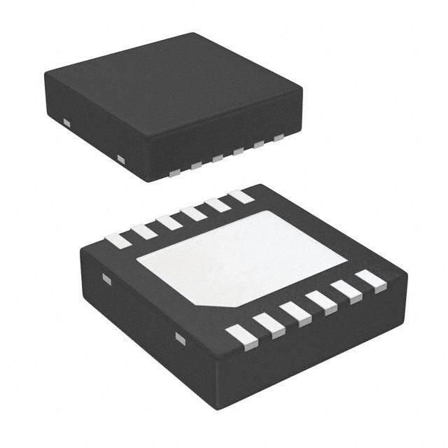
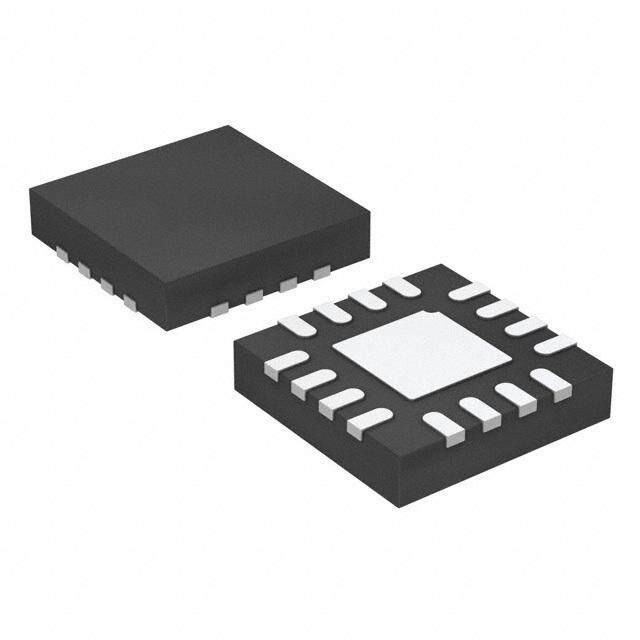
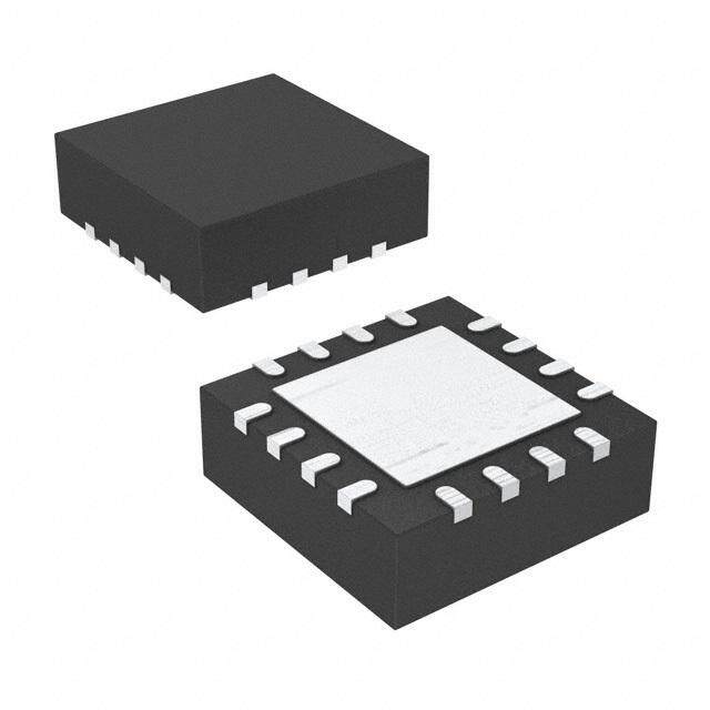
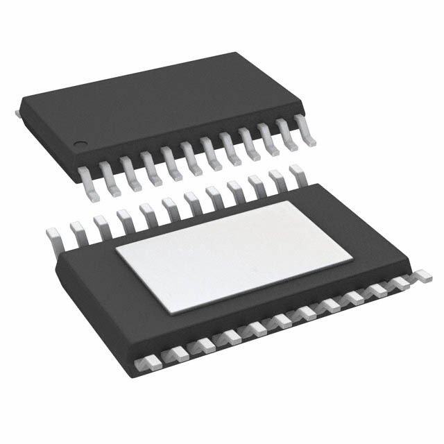
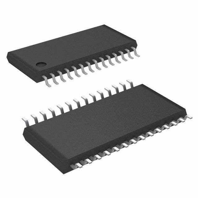
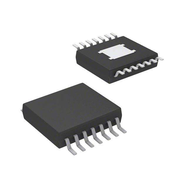
ICGOO电子元器件商城为您提供MSL1061AV-R由Atmel设计生产,在icgoo商城现货销售,并且可以通过原厂、代理商等渠道进行代购。 MSL1061AV-R价格参考。AtmelMSL1061AV-R封装/规格:PMIC - LED 驱动器, LED Driver IC 6 Output DC DC Regulator Step-Up (Boost) Analog, PWM Dimming 30mA 28-TQFN (5x5)。您可以下载MSL1061AV-R参考资料、Datasheet数据手册功能说明书,资料中有MSL1061AV-R 详细功能的应用电路图电压和使用方法及教程。
| 参数 | 数值 |
| 产品目录 | 集成电路 (IC) |
| 描述 | IC LED DRVR 6 CHAN PWM 28TQFN |
| 产品分类 | |
| 品牌 | Atmel |
| 数据手册 | |
| 产品图片 | |
| 产品型号 | MSL1061AV-R |
| rohs | 无铅 / 符合限制有害物质指令(RoHS)规范要求 |
| 产品系列 | - |
| 产品培训模块 | http://www.digikey.cn/PTM/IndividualPTM.page?site=cn&lang=zhs&ptm=25647http://www.digikey.cn/PTM/IndividualPTM.page?site=cn&lang=zhs&ptm=25677http://www.digikey.cn/PTM/IndividualPTM.page?site=cn&lang=zhs&ptm=25686 |
| 供应商器件封装 | 28-TQFN |
| 其它名称 | MSL1061AV-RDKR |
| 内部驱动器 | 是 |
| 包装 | Digi-Reel® |
| 安装类型 | 表面贴装 |
| 封装/外壳 | 28-WFQFN 裸露焊盘 |
| 工作温度 | -40°C ~ 85°C |
| 恒压 | - |
| 恒流 | - |
| 拓扑 | PWM,升压(升压) |
| 标准包装 | 1 |
| 电压-电源 | 4.75 V ~ 36 V |
| 电压-输出 | 48V |
| 类型-初级 | 背光,通用 |
| 类型-次级 | RGB,白色 LED |
| 输出数 | 6 |
| 频率 | 990kHz ~ 1.21MHz |






- 商务部:美国ITC正式对集成电路等产品启动337调查
- 曝三星4nm工艺存在良率问题 高通将骁龙8 Gen1或转产台积电
- 太阳诱电将投资9.5亿元在常州建新厂生产MLCC 预计2023年完工
- 英特尔发布欧洲新工厂建设计划 深化IDM 2.0 战略
- 台积电先进制程称霸业界 有大客户加持明年业绩稳了
- 达到5530亿美元!SIA预计今年全球半导体销售额将创下新高
- 英特尔拟将自动驾驶子公司Mobileye上市 估值或超500亿美元
- 三星加码芯片和SET,合并消费电子和移动部门,撤换高东真等 CEO
- 三星电子宣布重大人事变动 还合并消费电子和移动部门
- 海关总署:前11个月进口集成电路产品价值2.52万亿元 增长14.8%



PDF Datasheet 数据手册内容提取
Atmel LED Drivers MSL1061/MSL1064 6-string PWM LED Driver with Digitally Compensated, 1.1MHz, 48V Boost Regulator, ±1.5% Current Balance, I2C Interface Datasheet Brief
Atmel LED Drivers-MSL1061/MSL1064 6-string PWM LED Driver with Digitally Compensated, 1.1MHz, 48V Boost Regulator, ±1.5% Current Balance, I2C Interface The MSL1061/64 incorporates a current mode PWM boost regulator with 50V internal switch and a wide, 4.75V to 36V input voltage range. The General Description 1.1MHz switching frequency uses a small-sized inductor and output capacitors while maintaining high efficiency and low ripple voltage and noise. The boost regulator uses digital control and requires no external compensation. The Atmel® LED Drivers- An I2C/SMB compatible serial interface operates up to 1MHz, giving access to internal 8-bit PWM dimming and 4-bit analog current adjustment for 12- MSL1061 and MSL1064 are bit current control. Individual string enable and fault reporting are available. LED drivers with integrated The MSL1061 operates with one of four I2C slave addresses selected from a boost regulators capable of single input pin (AD0), whereas the lower cost MSL1064 has one fixed I2C slave address. driving six LED strings at The MSL1061/64 is also easy to employ without using an I2C interface, 30mA up to 48V for lighting dimming with an external PWM signal. applications to 8W, allowing Analog dimming of LED string current is available for use with an ambient up to 72 LEDs per driver light sensor (ALS) and/or temperature management with a thermistor or IC backlighting applications. temperature sensor. The MSL1064 comes in a 5 x 5mm, 24-pin TQFN package, and the MSL1061 in a 5 x5mm, 28-pin TQFN. Both packages are lead-free, halogen-free and RoHS-compliant, and operate over a -40°C to 85°C temperature range. Applications Long Life, Efficient LED Backlighting for: • Notebook PCs and Desktop PC Monitors • Medical and Industrial Instrumentation • Portable Media Players (PMPs) • Automotive Audio-visual Displays Traffic Lights Signage Ordering Information PART DESCRIPTION PACKAGE MSL1061AV 6-ch LED driver 28-pin, 5x5x0.75mm TQFN MSL1064AW 6-ch LED driver 24-pin, 5x5x0.75mm TQFN 2 Atmel LED Drivers-MSL1061/MSL1064
Atmel LED Drivers-MSL1061/MSL1064 6-string PWM LED Driver with Digitally Compensated, 1.1MHz, 48V Boost Regulator, ±1.5% Current Balance, I2C Interface Key Features • Drives 6 Strings of up to 12 LEDs per String • Individual Open-circuit and Short-circuit Fault Detection • Drives 72 White LEDs at 30mA for 8W Backlight • Faults Automatically Disable the Faulty String • Better than ±1.5% String-to-string Current Accuracy • Fault Reporting and Fault Reset Through I2C/SMB • 4.75V to 36V Wide Input Supply Range • FLTB Logic Output Indicates Faults • Integrated Boost Regulator with 50V Internal Switch • Enable Input Simplifies Operation Without I2C/SMB • 1.1MHz Current Mode PWM Boost for Low Noise • PWM Input Synchronizes PWM to System Clock • Up to 92% Boost Converter Efficiency and Allows Logic PWM Control Without I2C • Internal, Automatic Power Supply Management • Adjustable Over-voltage Protection • Adjustable LED Current up to 30mA per String • Serial I2C/SMB Compatible Interface to 1MHz • String Outputs can be Paralleled for >30mA LEDs • Four selectable I2C Slave Addresses (MSL1061) • 256:1 Internal PWM Dimming Range Through I2C • GUI Software for Ease of Evaluation • 16:1 Internal Analog Dimming Range Through I2C • -40°C - +85°C Operating Temperature Range • 12-Bit Total Internal PWM + Analog Dimming Range • Lead-free, Halogen-free, RoHS-compliant Package • ALS Interface for Automatic Brightness Setting • NTC Interface for Temperature Derating Application Circuit VIN = 4.75V to 36V VOUT = 48V max VIN SW …. EN OVP Up to 12 Fault White Alert FLTB LEDs per String OSC ILED Set String current MSL1061 ST.R 0 MSL1064 .. 1.5% maximum current ALS or . mismatch between NTC IADJ STR5 Strings SDA I C or PWM SCL SMBus I C address selection AD0 GND (MSL1061 only) Atmel LED Drivers-MSL1061/MSL1064 3
Quick Start Guide The maximum number of LEDs allowed in a string is determined by the maximum voltage rating of the boost This section summarizes for quick evaluation regulator’s internal power FET, which is 50V minus 2V the capabilities of, and differences between, the for switching noise transients, leaving 48V. The FET MSL1061 and MSL1064. is protected by the OVP trip, which has a 2% voltage tolerance, plus another 1% for the external setting The MSL1061 and MSL1064 are LED string drivers resistors R8 and R9 (Figure 6 on page 15) reducing the with integrated boost regulators, which power, monitor, maximum voltage to 46.5V. The total voltage needed and dim multiple LEDs at high efficiency for backlighting to drive a string is the forward voltage drop across the and signage applications. Each MSL1061/64 contains six desired LED strings, plus the headroom needed across outputs, each capable of sinking up to 30mA through a a string output’s current sink (600mV) to maintain string of series-connected LEDs. regulation, plus the boost regulator’s rectifier forward voltage (normally under 900mV) leaves 46.5V - 0.6V - How Many LEDs Can the Atmel LED 0.9V = 45V maximum for the LED string. The number of LEDs that the MSL1061/4 can drive per string is 45V / Drivers-MSL1061/64 Drive? {maximum LED forward voltage per LED}, or 12 LEDs The MSL1061/64 includes 6 current sinks (STR0 per string using 3.75V maximum forward voltage LEDs. through STR5) that each control the LED current of multiple series-connected white LEDs. Any combination Differences Between Atmel LED of the 6-strings may be enabled, and not all the strings Drivers-MSL1061/64 need to be used. Use the MSL1061 for applications where multiple Make sure that each enabled string contain the same drivers are connected to a single I2C bus such as RGB number of the same type of LED so that the total voltage and RGGB lighting. Use the lower cost MSL1064 for drop for each string is the same because the single boost single-driver applications, and multi-driver applications regulator supplies power to all six strings. Use a single that do not require all drivers on the same I2C MSL1061/64 LEDs of a single color/chemistry, such interface (Table 1). as white LED backlighting or single-color signage. For multicolor applications (e.g. RG, RGB, RGGB, RGBA), use separate MSL1061/64s per LED color/chemistry type. Each MSL1061/64 manages its integrated boost regulator to optimize efficiency for its strings of identical LEDs with matched electrical characteristics. 4 Atmel LED Drivers-MSL1061/MSL1064
Atmel LED Drivers-MSL1061/MSL1064 6-string PWM LED Driver with Digitally Compensated, 1.1MHz, 48V Boost Regulator, ±1.5% Current Balance, I2C Interface Table 1. Atmel LED Drivers-MSL1061 and MSL1064 Comparison FEATURE MSL1061 MSL1064 APPLICATION AND SUITABILITY 4 selectable slave addresses by Only one MSL1064 is uniquely I2C interface 1 fixed slave address (0x62) AD0 pin (0x60, 0x61, 0x62, 0x63) addressed on an I2C bus 28-lead, 5mm x 5mm TQFN, 24-lead, 5mm x 5mm TQFN, Package 0.5mm pitch 0.65mm pitch 0.2mm min gap between SW pins 0.6mm min total gap between SW IPC- If compliance is necessary use and adjacent conductors. Compliant pins and adjacent conductors. 2221A-2003 the MSL1064 or MSL1061 with to 100V with board coating, 15V Compliant to 100V with or without compliance board coating. without coating board coating Capabilities With and Without Using the Serial Interface MSL1061/64 operates as stand alone LED drivers with full digital (PWM) and analog (DAC) LED brightness control and fault reporting through I/O controls. Alternatively, LED dimming and fault reporting is managed over an I2C or SMB serial interface, allowing software/firmare LED intensity control. More detailed fault management reporting and software controlled shutdown (Table 2) via the serial interface. Table 2. Atmel LED Drivers-MSL1061/64 Stand Alone Capabilities and I2C Controlled Features FUNCTION CONTROLS AVAILABLE ON PINS ADDITIONAL CONTROLS AVAILABLE VIA I2C Global on/off control EN pin (Table 3 on page 9) Run mode/sleep mode Individual LED string on/off control Not available String enables register Analog LED current adjustment ILED pin (Table 3 on page 8) Current setting register PWM frequency register PWM LED current adjustment PWM pin (Table 3 on page 8) PWM duty ratio register Ambient light sensor (ALS) and/ or auto-matic temperature LED IADJ pin (Table 3 on page 9) Current setting register current adjustment FLTB pin indicates open-string, shorted- Status register identifies open/short circuit and over- Fault monitoring string, and over-temperature faults temperature faults to individual strings Atmel LED Drivers-MSL1061/MSL1064 5
Packages and Pin Connections Atmel LED Drivers-MSL1061/64 – 24-pin, 5mm x 5mm x 0.75mm TQFN package with 0.65mm lead pitch N N C W W C VI E N/ S S N/ 24 23 22 21 20 19 VCC 1 18 OVP VDD 2 17 STR0 TEST1 3 16 STR1 Figure 1. 24-pin, 5mm x 5mm x 0.75mm TQFN (0.65mm pin pitch) with Exposed Pad MSL1064 TEST2 4 15 STR2 SDA 5 (TOP VIEW) 14 STR3 SCL 6 13 STR4 7 8 9 10 11 12 M B C D J 5 W T S E D R L O L A T P F I I S Figure 2. 24-pin TQFN Package Dimensions 6 Atmel LED Drivers-MSL1061/MSL1064
Atmel LED Drivers-MSL1061/MSL1064 6-string PWM LED Driver with Digitally Compensated, 1.1MHz, 48V Boost Regulator, ±1.5% Current Balance, I2C Interface VIN EN SW SW SW SW N/C 28 27 26 25 24 23 22 VCC 1 21 OVP VDD 2 20 TEST3 TEST1 3 19 STR0 Figure 3. 28-pin, 5mm x 5mm x 0.75mm TQFN (0.5mm pin pitch) with Exposed Pad TEST2 4 MSL1061 18 STR1 SDA 5 (TOP VIEW) 17 STR2 SCL 6 16 STR3 AD0 7 15 STR4 8 9 10 11 12 13 14 M B C C D J 5 W LT OS N/ LE AD TR P F I I S Figure 4. 28-pin TQFN Package Dimensions Atmel LED Drivers-MSL1061/MSL1064 7
Pin Descriptions Table 3. Pin Assignments PIN NAME MSL1061 MSL1064 PIN DESCRIPTION 6V internal linear regulator output VCC powers the internal power FET switch driver. Bypass VCC to GND either with a 10µF or greater ceramic capacitor, or with a 10µF or VCC 1 1 greater tantalum capacitor in parallel with a 1µF ceramic capacitor. If the voltage at VIN is less than 6.5V, connect VCC directly to VIN to bypass the internal linear regulator, and power the driver directly from VIN 2.9V internal linear regulator output VDD 2 2 VDD powers internal logic. Bypass VDD to GND with at least a 4.7µF ceramic capacitor TEST1 3 3 Factory test connection. Leave unconnected TEST2 4 4 Factory test connection. Connect to GND I²C serial data I/O SDA 5 5 SDA is the data I/O for the I²C serial interface I²C serial clock input SCL 6 6 SCL is the clock input for the I²C serial interface I²C slave ID selection input AD0 7 - For MSL1061, connect AD0 to GND, VDD, SCL, or SDA to set the I²C slave ID to 0x60, 0x61, 0x62, or 0x63. The MSL1064 I²C slave ID is fixed at 0x62, and is not user-selectable PWM control input PWM 8 7 Drive PWM with a PWM signal up to 40kHz to pulse-width-modulate the LED current Fault indication output (active low) FLTB sinks current to GND whenever the MSL1061/64 detects a fault. FLTB 9 8 Once a fault is detected, FLTB remains low until EN is toggled low/high, input power is cycled off/on, or the fault status is reset through the I²C interface. Oscillator control input OSC 10 9 Connect a 115kΩ, 1% resistor from OSC to GND to set the internal oscillator frequency to 11MHz and the boost regulator switching frequency to 1.1MHz TEST3 11 - Factory test connection with internal 1.8kΩ pull-up to VDD. Leave unconnected Maximum LED current control input Connect a resistor from ILED to GND to set the full-scale LED string current. ILED 12 10 For example, connect a 100kΩ resistor to GND to set a 20mA sink current through each LED string 8 Atmel LED Drivers-MSL1061/MSL1064
Atmel LED Drivers-MSL1061/MSL1064 6-string PWM LED Driver with Digitally Compensated, 1.1MHz, 48V Boost Regulator, ±1.5% Current Balance, I2C Interface PIN NAME MSL1061 MSL1064 PIN DESCRIPTION Analog LED current dimming input IADJ 13 11 Apply a voltage between 0V to 1.22V to linearly control the LED current from 0 to 100%. Connect IADJ to VDD if unused LED string 5 current sink output STR5 14 12 Connect the cathode of LED String 5 to STR5. Connect STR5 to GND if unused LED string 4 current sink output STR4 15 13 Connect the cathode of LED String 4 to STR4. Connect STR4 to GND if unused LED string 3 current sink output STR3 16 14 Connect the cathode of LED String 3 to STR3. Connect STR3 to GND if unused LED string 2 current sink output STR2 17 15 Connect the cathode of LED String 2 to STR2. Connect STR2 to GND if unused LED string 1 current sink output STR1 18 16 Connect the cathode of LED String 1 to STR1. Connect STR1 to GND if unused LED string 0 current sink output STR0 19 17 Connect the cathode of LED String 0 to STR0. Connect STR0 to GND if unused Overvoltage detection input OVP 21 18 Connect a resistive voltage divider from the boost output voltage to OVP to set the overvoltage protection set point. OVP threshold is 1.28V N/C 22 19 No internal connection. Leave unconnected 23, 24, 25, Drain of the internal boost power MOSFET switch SW 20, 21 26 Connect all SW pins together and to the boost regulator inductor and rectifier N/C - 22 No internal connection. Leave unconnected Enable input (active high) EN 27 23 Drive EN high to turn on the MSL1061/64, and drive it low to turn it off. For automatic startup, connect EN to VIN through a 100kΩ resistor Supply voltage input Connect the input supply voltage to VIN. VIN 28 24 VIN powers the internal linear regulator that powers VCC. Bypass VIN to GND with a 1µF or greater ceramic capacitor Exposed Exposed GND Ground pad pad Atmel LED Drivers-MSL1061/MSL1064 9
Absolute Maximum Ratings Voltage (With Respect to GND Exposed Pad on Package Underside) VIN ................................................................................................................................................................................................................. -0.3V to +40V VCC, EN.........................................................................................................................................................................................................-0.3V to +8V VDD, OVP, IADJ, FLTB, ILED, SDA, SCL, AD0, OSC, PWM .................................................................-0.3V to +3.6V SW ................................................................................................................................................................................................................ -0.3V to +50V STR0, STR1, STR2, STR3, STR4, STR5 ................................................................................................................... -0.3V to +45V Current (Into Pin) SW ............................................................................................................................................................................................................................................±3A STR0, STR1, STR2, STR3, STR4, STR5 .................................................................................................................................... ±35mA All other pins ..........................................................................................................................................................................................................±20mA Continuous Power Dissipation at 70°C 24-Pin TQFN (see Note 8, Note 9) ........................................................................................................................................2286mW 28-Pin TQFN (see Note 8, Note 9) ........................................................................................................................................2286mW Ambient Operating Temperature Range T = T to T ..................................................... -40°C to +85°C A MIN MAX Junction Temperature ............................................................................................................................................................................ +125°C Storage Temperature Range ................................................................................................................................... -65°C to +125°C Lead Soldering Temperature, 10s ..............................................................................................................................................+300°C 10 Atmel LED Drivers-MSL1061/MSL1064
Atmel LED Drivers-MSL1061/MSL1064 6-string PWM LED Driver with Digitally Compensated, 1.1MHz, 48V Boost Regulator, ±1.5% Current Balance, I2C Interface Electrical Characteristics (Circuit of Figure 6, V = 12V, default register settings of Table 7, T = -40°C to +85°C, unless otherwise noted. Typical values are at T = +25°C) (Note 1) VIN A A PARAMETER CONDITIONS AND NOTES MIN TYP MAX UNIT DC ELECTRICAL CHARACTERISTICS V = V 4.75 6.5 V VIN operating supply voltage VIN VCC VCC unconnected 6.5 36 V V = 12V 4 14 mA VIN quiescent supply current V = 3V, V = 0V VIN EN PWM V = 6V, V = 6V 4 14 mA VIN VCC VIN shutdown supply current V = V = 0V 1 4 10 µA EN PWM VCC output voltage 5.6 6 6.3 V VCC line regulation 6.5V < V < 36V 1 2 5 mV VIN VCC dropout voltage V = 6V, I = 5mA, V = 0V 100 300 550 mV VIN VCC PWM VCC short-circuit current V = 0V 30 80 150 mA VCC VCC UVLO threshold V rising, hysteresis = 150mV 4.1 4.3 4.5 V VCC VDD output voltage I = 1mA 2.7 2.9 3.1 V VDD VDD short-circuit current V = 0V 10 35 60 mA VDD VDD UVLO threshold V rising, hysteresis = 80mV 2.4 2.5 2.6 V VDD Thermal shutdown threshold (rising) 135 °C Thermal shutdown hysteresis 10 °C PARAMETER CONDITIONS AND NOTES MIN TYP MAX UNIT DC ELECTRICAL CHARACTERISTICS - LED CURRENT CONTROL STR0 TO STR5 ILED regulation voltage R5 = 100kΩ 1.195 1.22 1.245 V STR0 to STR5 full scale sink current V = 1V, R5 = 100kΩ, V = V = 3V 19.7 20 20.3 mA STRn IADJ PWM V = 1V, R5 = 60kΩ, V = V = 3V STR0 to STR5 maximum sink current STRn IADJ PWM 30 mA (Note 10) STR0 to STR5 current matching V = 1V, R5 = 100kΩ, V = 3V (Note 11) 1.5 % STRn PWM V = 0V, V = 40V 0.1 1 µA STR0 to STR5 leakage current EN STRn V = 3V, V = 40V, V = 3V 0.1 1 µA EN STRn PWM STR0 to STR5 short circuit detection threshold 4 4.4 4.8 V STR0 to STR5 open circuit detection threshold 0.1 V PARAMETER CONDITIONS AND NOTES MIN TYP MAX UNIT DC ELECTRICAL CHARACTERISTICS - LOGIC I/OS EN logic high input voltage 2.3 V EN logic low input voltage 0.8 V EN logic input current V = 3V 20 µA EN Atmel LED Drivers-MSL1061/MSL1064 11
PARAMETER CONDITIONS AND NOTES MIN TYP MAX UNIT Between EN input package pin and internal EN logic input series resistance 10.5 kΩ Zener clamp EN logic input Zener clamp 5.8 V SCL, SDA, AD0, 2 V PWM logic high input voltage SCL, SDA, AD0, 0.9 V PWM logic low input voltage SDA, SCL, AD0 input capacitance 10 pF SDA output low voltage Sinking 6mA 0.4 V FLTB output low voltage Sinking 1mA 0.1 0.2 V IADJ, FLTB, PWM, SCL, SDA, 10 µA AD0 leakage current PARAMETER CONDITIONS AND NOTES MIN TYP MAX UNIT DC ELECTRICAL CHARACTERISTICS - BOOST REGULATOR SW on resistance I = 100mA 0.4 0.6 Ω SW SW current limit 2 A OSC regulation voltage R4 = 115kΩ ±1% 1.195 1.22 1.245 V STR0-STR5 boost regulation voltage R5= 100kΩ, PWM=100% (Note 12) 600 mV OVP threshold V rising 1.25 1.28 1.31 V OVP OVP hysteresis 60 mV OVP leakage current V = 3.6V 1 µA OVP PARAMETER CONDITIONS AND NOTES MIN TYP MAX UNIT AC ELECTRICAL CHARACTERISTICS PWM input frequency 0 50 kHz PWM input duty ratio INTPWM bit D3=0 in control register to select 0 100 % external PWM input to be used for direct LED PWM input minimum string on time string dimming control 14 µs PWM input minimum string off time 3.2 µs PWM input frequency, external PWM clock mode INTPWM bit D3=1, EXTCLK bit D2=1 in 0 12 MHz control register to select external PWM PWM input duty ratio, external PWM clock mode input to be used as clock for internal PWM 30 70 % dimming control R4 = 115kΩ ±1%, INTPWM bit D3=1, EXTCLK bit D2=0 in control register to select PWM frequency (internal oscillator) 9 11 12 MHz internal oscillator to be used as clock for internal PWM dimming control Boost regulator switching frequency R4 = 115kΩ ±1% 0.99 1.1 1.21 MHz Boost regulator maximum duty ratio R4 = 115kΩ ±1% 89 92 % Boost regulator startup time 100 120 ms 12 Atmel LED Drivers-MSL1061/MSL1064
Atmel LED Drivers-MSL1061/MSL1064 6-string PWM LED Driver with Digitally Compensated, 1.1MHz, 48V Boost Regulator, ±1.5% Current Balance, I2C Interface PARAMETER SYMBOL CONDITIONS AND NOTES MIN TYP MAX UNIT I²C SWITCHING CHARACTERISTICS TOEN bit D1=0 in control register to disable bus 0 timeout SCL clock frequency 1/t 1000 kHz SCL TOEN bit D1=1 in control register to enable bus 0.066 timeout Bus time-out period t 15 25 ms TIMEOUT STOP to START condition bus t 0.5 µs free time BUF Repeated START condition t 0.26 µs hold time HD:STA Repeated START condition t 0.26 µs set-up time SU:STA STOP condition set-up time t 0.26 µs SU:STOP SDA data hold time t 5 ns HD:DAT SDA data valid acknowledge time t (Note 3) 0.05 0.55 µs VD:ACK SDA data valid time t (Note 4) 0.05 0.55 µs VD:DAT SDA data set-up time t 100 ns SU:DAT SCL clock low period t 0.5 µs LOW SCL clock high period t 0.26 µs HIGH SDA, SCL fall time t (Note 5, Note 6) 120 ns F SDA, SCL rise time t 120 ns R SDA, SCL input suppression t (Note 7, Note 10) 50 ns filter period SP Note 1. All parameters are tested at T=25°C, unless otherwise noted. Specifications at temperature are guaranteed by design A Note 2. Minimum SCL clock frequency is limited by the bus timeout feature, which resets the serial bus interface if either SDA or SCL is held low for t . Disable the bus timeout feature for DC operation timeout Note 3. t = SCL LOW to SDA (out) low acknowledge time VD:ACK Note 4. t = minimum SDA output data-valid time following SCL low transition VD:DAT Note 5. A master device must internally provide an SDA hold time of at least 300ns to ensure an SCL low state Note 6. The maximum SDA and SCL rise times is 300ns. The maximum SDA fall time is 250ns. This allows series protection resistors to be connected between SDA and SCL inputs and the SDA/SCL bus lines without exceeding the maximum allowable rise time Note 7. MSL1061/64 includes input filters on SDA, SCL, and AD0 inputs that suppress noise less than 50ns Note 8. Subject to thermal dissipation characteristics of the device Note 9. When mounted according to JEDEC JEP149 and JESD51-12 for a two-layer PCB, θ = 24.1°C/W, and θ = 2.7°C/W JA JC Note 10. Guaranteed by design and characterization. Not production tested Note 11. STR0 to STR5 current matching is the difference of any one string current and the average of all string currents divided by the average of all string currents Note 12. The MSL1061/64 selects the string (STR0 through STR5) with the lowest voltage to control the boost regulator voltage Atmel LED Drivers-MSL1061/MSL1064 13
BlockDiagram The block diagram for the 28-pin MSL1061 is shown in Figure 5. The differences for the 24-pin MSL1064 are that the MSL1064 provides only two pins for SW instead of four pins on the MSL1061, and the AD0 pin is not pinned out but is instead bonded internally to SCL. The MSL1061 I2C slave address is selected using AD0 from one of the four address pairs, 0xC0/0xC1 - 0xC6/0xC7, whereas the MSL1064 I2C slave address is fixed at 0xC4/0xC5. Figure 5. Atmel LED Driver-MSL1061 Block Diagram 14 Atmel LED Drivers-MSL1061/MSL1064
Typical Application Circuit Figure 6. Backlight Example Driving 60 White LEDs 4.7 Table 4. Typ. Application Circuit Parameters Table 5. Typ. Application Circuit Bill of Materials PARAMETER VALUE VENDOR PART COMPONENT DESCRIPTION NUMBER Minimum input voltage 4.75V C4, C5, C6, C7* 1µF, 50V, X7R Maximum input voltage (set by 30V minimum LEDs string voltage) 10µF, 10V, X7R or C2 tantalum (see note) Number of LEDs 60 C3 33µF, 35V, X7R Number of LED strings 6 C1 4.7µF, 6.3V, X7R Number of LED per string 10 R8 1MΩ, 1% LED forward current (set by R5) 20mA R9 28.7kΩ, 1% Osram LW- White LED Y3SG R4 115kΩ, 1% Minimum LED forward voltage 2.9V R5 100kΩ, 1% Typical LED forward voltage 3.3V R7 100kΩ, 5% Maximum LED forward voltage 3.6V R2 1MΩ, 5% Minimum LED string voltage 29V L1 10µH, 1.7A Sumida CDRH6D28-100 Maximum LED string voltage 36V Central Semi D1 60V, 2A Schottky CMSH2-60M Oscillator frequency (set by R4) 1.1MHz LEDs 60 x 30mA LED Osram LW-Y2SG Overvoltage protection (OVP) trip 45.9V point (set by R8 and R9) LED driver MSL1060 MSL1060 * Note: C7 is only required if tantalum capacitor is used for C2 Atmel LED Drivers-MSL1061/MSL1064 15
Detailed Description The MSL1061/64 is an LED driver with integrated boost Internal Oscillator - R4 regulator for driving an array of LEDs with up to 8W of The MSL1061/64 uses an internal oscillator with power. The I²C/SMB serial interface, logic controls, and frequency set by resistor R4 from OSC to GND (Figure fault management make the MSL1061/64 especially 6). Use 115kΩ ±1% resistance value for R4. This sets suited to drive up to 72 white LEDs for portable device the internal LED dimming PWM frequency to 11MHz backlighting. It is also ideal for industrial lighting and and the boost regulator PWM frequency to 1.1MHz. signage applications, and can, for example, drive a 6 When using different values for R4 the MSL1061/64 string x 18 series LED array totaling 108 red LEDs performance is not guaranteed. (2.5V LED forward voltage drop). The MSL1061/64 includes six current sinks (STR0 Setting the Full-scale LED String Current - R5 through STR5) that each control the LED current of series-connected LEDs. A built-in step-up (boost) R5 sets the full-scale static LED current for all enabled regulator supplies power to the LEDs. The MSL1061/64 strings (Figure 6) from ILED to GND. The maximum full- controls the output voltage of the boost regulator such scale LED current is 30mA. The equation for calculating that all LED strings have sufficient voltage to maintain external resistor R5 (Figure 6) to set the full-scale LED regulated LED current. This control loop operates string current I is: ILED automatically without any user interaction or set-up. 2000 I = Application Information ILED R5 VCC and VDD Regulators where R5 is in kilohms and ILED is in milliamperes. The MSL1061/64 includes two linear voltage regulators A value of 100kΩ for resistor R5 sets 20mA full-scale to generate the internal voltage rails, VDD and VCC. The LED current. The minimum allowed value for R5 is regulators allow the MSL1061/64 to operate directly 66.7kΩ, which sets 30mA full-scale LED current. from the same higher voltage supply, VIN, which supplies Reduce the static LED current from full-scale using the the LED boost regulator. Use the VDD and VCC regulators LED string current register. This register reduces LED only to power the MSL1061/64’s internal circuitry, current proportional to the 4-bit IDAC register. therefore do not draw any external current from them. The VCC regulator generates a nominally 6V rail from VIN. VCC powers the boost regulator’s power switch and the VDD regulator. Bypass VCC to GND either with a 10µF or greater ceramic capacitor or with a 10µF or greater tantalum capacitor in parallel with a 1µF ceramic capacitor. In applications where there is a local 4.75V to 6.5V supply available, power VCC and VIN directly from this supply. In this case use this supply or a separate higher voltage supply to power the LED boost regulator. When using a higher voltage supply connect it to the inductor, L1 (Figure 6), and not to the MSL1061/64. The VDD regulator generates a nominally 2.9V rail from VCC. VDD operates the internal low-voltage circuits. Bypass VDD to GND with a 4.7µF or greater capacitor. 16 Atmel LED Drivers-MSL1061/MSL1064
Atmel LED Drivers-MSL1061/MSL1064 6-string PWM LED Driver with Digitally Compensated, 1.1MHz, 48V Boost Regulator, ±1.5% Current Balance, I2C Interface Boost Regulator Components Boost Supply Over-voltage Protection (OVP) - R8 and R9 The boost regulator is internally compensated, includes an internal high voltage power switch, and requires only The OVP input sets the boost regulator’s output voltage an inductor, rectifier, and bypass capacitors. The current- upper limit, and protects the boost regulator from an mode boost regulator operates in either continuous open-circuit LED fault. Set the OVP voltage V by TRIP conduction mode (CCM) or discontinuous conduction resistors R8 and R9 (Figure 6): mode (DCM). In CCM, the inductor current does not fall to zero when operating at full power, keeping inductor (R8+R9) ripple current low and switching noise at a minimum. V =V The boost regulator switching frequency is 1.1MHz set TRIP OVP R9 by the 115kΩ resistor R4 from OSC pin to GND (Figure 6). Select the inductor, rectifier diode, and output where V =1.28V, nominal. capacitors per the following guidelines. OVP To minimize losses in the rectifier, choose one with fast switching and low forward voltage drop. Ensure that the rectifier can withstand a reverse voltage equal to the regulator output voltage. The average forward current is equal to the total LED string current (for example 6 strings x 30mA = 180mA), while the peak current is equal to the inductor peak current (2A). The boost output capacitor holds the voltage at the output of the boost regulator while the internal power switch is on and the rectifier is not conducting. Use ceramic capacitors for small size and high ripple current capacity, and derate them for operating voltage because of the voltage coefficient of capacitance which decreases the effective capacitance with increased operating voltage. Use two parallel-connected 1µF 100V X7R ceramic capacitors and a 10µH inductor with a 1.7A peak current rating. Atmel LED Drivers-MSL1061/MSL1064 17
Register Map Summary Control the MSL1061/64 through an I2C interface using nine registers (Table 6). The power-up defaults (Table 7) are such that an MSL1061/64 operates as a standalone LED driver if the I2C interface is not used. The Internal register addressing auto-increments through the register map allowing sequential reads or writes without needing to write separate addresses for each byte. Table 6. Atmel LED Drivers-MSL1061/64 Register Map REGISTER DATA REGISTER FUNCTION ADDRESS D7 D6 D5 D4 D3 D2 D1 D0 Run/sleep MSTRCNTRL 0x00 - - - - - - - SLEEP mode PWM source, I2C/ SMB bus CNTRL 0x01 - - - - INTPWM EXTCLK TOEN FLTEN timeout, fault pin enable WRITES TO THIS REGISTER ADDRESS ARE IGNORED, - UNUSED 0X02 AND READS RETURN THE VALUE 0X00 Fault status STATUS 0x03 - OTDET SCDET OCDET - - - FLTDET summary Open circuit OCSTATUS 0x04 - - OC5 OC4 OC3 OC2 OC1 OC0 fault status Short circuit SCSTATUS 0x05 - - SC5 SC4 SC3 SC2 SC1 SC0 fault status PWM PWMFREQ frequency 0x06 D7 D6 D5 D4 D3 D2 D1 D0 prescaler PWM duty PWMDUTY 0x07 D7 D6 D5 D4 D3 D2 D1 D0 ratio WRITES TO THIS REGISTER ADDRESS ARE IGNORED, - UNUSED 0X08 AND READS RETURN THE VALUE 0X00 String STREN 0x09 - - STR5EN STR4EN STR3EN STR2EN STR1EN STR0EN enables - unused 0x0A writes to this register address are ignored, and reads return the value 0x00 - unused 0x0B writes to this register address are ignored, and reads return the value 0x00 - unused 0x0C writes to this register address are ignored, and reads return the value 0x00 - unused 0x0D writes to this register address are ignored, and reads return the value 0x00 - unused 0x0E writes to this register address are ignored, and reads return the value 0x00 - unused 0x0F writes to this register address are ignored, and reads return the value 0x00 LED string IDAC 0x10 - - - - DAC3 DAC2 DAC1 DAC0 current 18 Atmel LED Drivers-MSL1061/MSL1064
Atmel LED Drivers-MSL1061/MSL1064 6-string PWM LED Driver with Digitally Compensated, 1.1MHz, 48V Boost Regulator, ±1.5% Current Balance, I2C Interface Register Map Power-up Defaults Table 7. Atmel LED Drivers-MSL1061/64 Register Power-up Defaults REGISTER DATA REGISTER POWER-UP CONDITION ADDRESS D7 D6 D5 D4 D3 D2 D1 D0 MSTRCNTRL Run mode 0x00 0 0 0 0 0 0 0 0 Fault detection is enabled I²C bus timeout is disabled PWM internal 11MHz clock is used, CNTRL 0x01 0 0 0 0 0 0 0 1 prescaled by PWMFREQ PWM control is by PWM pin. PWMDUTY register is ignored No faults (open, short, or temperature) STATUS 0x03 0 0 0 0 0 0 0 0 are detected None of the six LED outputs STR0 to OCSTATUS 0x04 0 0 0 0 0 0 0 0 STR5 has an open circuit fault None of the six LED outputs STR0 to SCSTATUS 0x05 0 0 0 0 0 0 0 0 STR5 has a short circuit fault Internal PWM frequency is the PWMFREQ 0x06 0 0 0 0 0 0 0 0 maximum 43kHz PWMDUTY Internal PWM duty ratio is 0.39% 0x07 0 0 0 0 0 0 0 0 All of the six LED outputs STR0 to STREN 0x09 0 0 1 1 1 1 1 1 STR5 are enabled LED string current is 100% of the value IDAC 0x10 0 0 0 0 1 1 1 1 programmed by resistor R5 Atmel LED Drivers-MSL1061/MSL1064 19
Atmel Corporation Atmel Asia Limited Atmel Munich GmbH Atmel Japan 2325 Orchard Parkway Unit 01-5 & 16, 19F Business Campus 9F, Tonetsu Shinkawa Bldg. San Jose, CA 95131 BEA Tower, Millennium City 5 Parkring 4 1-24-8 Shinkawa USA 418 Kwun Tong Road D-85748 Garching b. Munich Chuo-ku, Tokyo 104-0033 Tel: (+1)(408) 441-0311 Kwun Tong, Kowloon GERMANY JAPAN Fax: (+1)(408) 487-2600 HONG KONG Tel: (+49) 89-31970-0 Tel: (+81)(3) 3523-3551 www.atmel.com Tel: (+852) 2245-6100 Fax: (+49) 89-3194621 Fax: (+81)(3) 3523-7581 Fax: (+852) 2722-1369 © 2011 Atmel Corporation. All rights reserved. / Rev.: MEM-MSL1061/64DB1-E-US_06-11 Atmel®, logo and combinations thereof, and others are registered trademarks or trademarks of Atmel Corporation or its subsidiaries. Other terms and product names may be trademarks of others. Disclaimer: The information in this document is provided in connection with Atmel products. No license, express or implied, by estoppel or otherwise, to any intellectual property right is granted by this document or in connection with the sale of Atmel products. EXCEPT AS SET FORTH IN THE ATMEL TERMS AND CONDITIONS OF SALES LOCATED ON THE ATMEL WEBSITE, ATMEL ASSUMES NO LIABILITY WHATSOEVER AND DISCLAIMS ANY EXPRESS, IMPLIED OR STATUTORY WARRANTY RELATING TO ITS PRODUCTS INCLUDING, BUT NOT LIMITED TO, THE IMPLIED WARRANTY OF MERCHANTABILITY, FITNESS FOR A PARTICULAR PURPOSE, OR NON-INFRINGEMENT. IN NO EVENT SHALL ATMEL BE LIABLE FOR ANY DIRECT, INDIRECT, CONSEQUENTIAL, PUNITIVE, SPECIAL OR INCIDENTAL DAMAGES (INCLUDING, WITHOUT LIMITATION, DAMAGES FOR LOSS AND PROFITS, BUSINESS INTERRUPTION, OR LOSS OF INFORMATION) ARISING OUT OF THE USE OR INABILITY TO USE THIS DOCUMENT, EVEN IF ATMEL HAS BEEN ADVISED OF THE POSSIBILITY OF SUCH DAMAGES. Atmel makes no representations or warranties with respect to the accuracy or completeness of the contents of this document and reserves the right to make changes to specifications and products descriptions at any time without notice. Atmel does not make any commitment to update the information contained herein. Unless specifically provided otherwise, Atmel products are not suitable for, and shall not be used in, automotive applications. Atmel products are not intended, authorized, or warranted for use as components in applications intended to support or sustain life.

 Datasheet下载