ICGOO在线商城 > 分立半导体产品 > 晶体管 - FET,MOSFET - 射频 > MRFE6VS25NR1
 Datasheet下载
- 型号: MRFE6VS25NR1
- 制造商: Freescale Semiconductor
- 库位|库存: xxxx|xxxx
- 要求:
| 数量阶梯 | 香港交货 | 国内含税 |
| +xxxx | $xxxx | ¥xxxx |
查看当月历史价格
查看今年历史价格
MRFE6VS25NR1产品简介:
ICGOO电子元器件商城为您提供MRFE6VS25NR1由Freescale Semiconductor设计生产,在icgoo商城现货销售,并且可以通过原厂、代理商等渠道进行代购。 MRFE6VS25NR1价格参考¥177.56-¥231.11。Freescale SemiconductorMRFE6VS25NR1封装/规格:晶体管 - FET,MOSFET - 射频, 射频 Mosfet LDMOS 50V 10mA 512MHz 25.4dB 25W TO-270-2。您可以下载MRFE6VS25NR1参考资料、Datasheet数据手册功能说明书,资料中有MRFE6VS25NR1 详细功能的应用电路图电压和使用方法及教程。
| 参数 | 数值 |
| 产品目录 | |
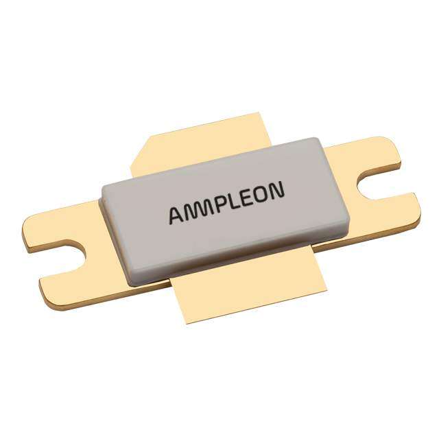
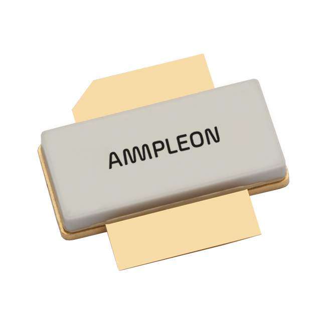
| 描述 | TRANS RF N-CH FET LDMOS TO270-2 |
| 产品分类 | RF FET |
| 品牌 | Freescale Semiconductor |
| 数据手册 | |
| 产品图片 |
|
| 产品型号 | MRFE6VS25NR1 |
| rohs | 无铅 / 符合限制有害物质指令(RoHS)规范要求 |
| 产品系列 | - |
| 供应商器件封装 | TO-270-2 |
| 其它名称 | MRFE6VS25NR1CT |
| 功率-输出 | 25W |
| 包装 | 剪切带 (CT) |
| 噪声系数 | - |
| 增益 | 25.4dB |
| 封装/外壳 | TO-270-2 |
| 晶体管类型 | LDMOS |
| 标准包装 | 1 |
| 电压-测试 | 50V |
| 电压-额定 | 133V |
| 电流-测试 | 10mA |
| 频率 | 1.8MHz ~ 2GHz |
| 额定电流 | - |


- 商务部:美国ITC正式对集成电路等产品启动337调查
- 曝三星4nm工艺存在良率问题 高通将骁龙8 Gen1或转产台积电
- 太阳诱电将投资9.5亿元在常州建新厂生产MLCC 预计2023年完工
- 英特尔发布欧洲新工厂建设计划 深化IDM 2.0 战略
- 台积电先进制程称霸业界 有大客户加持明年业绩稳了
- 达到5530亿美元!SIA预计今年全球半导体销售额将创下新高
- 英特尔拟将自动驾驶子公司Mobileye上市 估值或超500亿美元
- 三星加码芯片和SET,合并消费电子和移动部门,撤换高东真等 CEO
- 三星电子宣布重大人事变动 还合并消费电子和移动部门
- 海关总署:前11个月进口集成电路产品价值2.52万亿元 增长14.8%

PDF Datasheet 数据手册内容提取
Freescale Semiconductor DocumentNumber:MRFE6VS25N Technical Data Rev.1,12/2012 RF Power LDMOS Transistors High Ruggedness N--Channel MRFE6VS25NR1 Enhancement--Mode Lateral MOSFETs MRFE6VS25GNR1 RFpowertransistorsdesignedforbothnarrowbandandbroadbandISM, broadcastandaerospaceapplicationsoperatingatfrequenciesfrom1.8to 2000MHz.ThesedevicesarefabricatedusingFreescale’senhanced ruggednessplatformandaresuitableforuseinapplicationswherehigh 1.8--2000MHz,25W,50V VSWRsareencountered. WIDEBAND TypicalPerformance:VDD=50Volts RFPOWERLDMOSTRANSISTORS Frequency Pout Gps D IMD(1) (MHz) SignalType (W) (dB) (%) (dBc) 1.8to30(2,6) Two--Tone 25PEP 25 51 --30 (10kHzspacing) 30--512(3,6) Two--Tone 25PEP 17.1 30.1 --32 (200kHzspacing) TO--270--2 512(4) Pulse(100sec, 25Peak 25.4 74.5 — PLASTIC 20%DutyCycle) MRFE6VS25NR1 512(4) CW 25 25.5 74.7 — 1030(5) CW 25 22.5 60 — LoadMismatch/Ruggedness Frequency Pin Test (MHz) SignalType VSWR (W) Voltage Result TO--270--2GULL PLASTIC 30(2) CW >65:1 0.23 50 NoDevice MRFE6VS25GNR1 atallPhase (3dB Degradation Angles Overdrive) 512(3) CW 1.6 (3dB Overdrive) 512(4) Pulse 0.14Peak Gate 1 2 Drain (100sec,20% (3dB DutyCycle) Overdrive) 512(4) CW 0.14 (3dB Overdrive (TopView) 1030(5) CW 0.34 (3dB Note: The backside of the package is the Overdrive sourceterminalforthetransistor. 1. Distortionproductsarereferencedtooneoftwotones.Seep.13,20. Figure1.PinConnections 2. Measuredin1.8--30MHzbroadbandreferencecircuit. 3. Measuredin30--512MHzbroadbandreferencecircuit. 4. Measuredin512MHznarrowbandtestcircuit. 5. Measuredin1030MHznarrowbandtestcircuit. 6. Thevaluesshownaretheminimummeasuredperformancenumbersacrossthe indicatedfrequencyrange. Features WideOperatingFrequencyRange ExtremeRuggedness Unmatched,CapableofVeryBroadbandOperation IntegratedStabilityEnhancements LowThermalResistance ExtendedESDProtectionCircuit InTapeandReel.R1Suffix=500Units,24mmTapeWidth,13--inchReel. FreescaleSemiconductor,Inc.,2012.Allrightsreserved. MRFE6VS25NR1MRFE6VS25GNR1 RFDeviceData FreescaleSemiconductor,Inc. 1
Table1.MaximumRatings Rating Symbol Value Unit Drain--SourceVoltage VDSS --0.5,+133 Vdc Gate--SourceVoltage VGS --6.0,+10 Vdc StorageTemperatureRange Tstg --65to+150 C CaseOperatingTemperature TC --40to+150 C OperatingJunctionTemperature(1,2) TJ --40to+225 C Table2.ThermalCharacteristics Characteristic Symbol Value(2,3) Unit ThermalResistance,JunctiontoCase RJC 1.2 C/W CW:CaseTemperature80C,25WCW,50Vdc,IDQ=10mA,512MHz ThermalImpedance,JunctiontoCase ZJC 0.29 C/W Pulse:CaseTemperature77C,25WPeak,100secPulseWidth, 20%DutyCycle,50Vdc,IDQ=10mA,512MHz Table3.ESDProtectionCharacteristics TestMethodology Class HumanBodyModel(perJESD22--A114) 2,passes2500V MachineModel(perEIA/JESD22--A115) B,passes250V ChargeDeviceModel(perJESD22--C101) IV,passes2000V Table4.MoistureSensitivityLevel TestMethodology Rating PackagePeakTemperature Unit PerJESD22--A113,IPC/JEDECJ--STD--020 3 260 C Table5.ElectricalCharacteristics (TA=25Cunlessotherwisenoted) Characteristic Symbol Min Typ Max Unit OffCharacteristics Gate--SourceLeakageCurrent IGSS — — 400 nAdc (VGS=5Vdc,VDS=0Vdc) Drain--SourceBreakdownVoltage V(BR)DSS 133 142 — Vdc (VGS=0Vdc,ID=50mA) ZeroGateVoltageDrainLeakageCurrent IDSS — — 2 Adc (VDS=50Vdc,VGS=0Vdc) ZeroGateVoltageDrainLeakageCurrent IDSS — — 7 Adc (VDS=100Vdc,VGS=0Vdc) OnCharacteristics GateThresholdVoltage VGS(th) 1.5 2.0 2.5 Vdc (VDS=10Vdc,ID=85Adc) GateQuiescentVoltage VGS(Q) 2.0 2.4 3.0 Vdc (VDD=50Vdc,ID=10mAdc,MeasuredinFunctionalTest) Drain--SourceOn--Voltage VDS(on) — 0.28 — Vdc (VGS=10Vdc,ID=210mAdc) DynamicCharacteristics ReverseTransferCapacitance Crss — 0.26 — pF (VDS=50Vdc30mV(rms)ac@1MHz,VGS=0Vdc) OutputCapacitance Coss — 14.2 — pF (VDS=50Vdc30mV(rms)ac@1MHz,VGS=0Vdc) InputCapacitance Ciss — 39.2 — pF (VDS=50Vdc,VGS=0Vdc30mV(rms)ac@1MHz) 1. ContinuoususeatmaximumtemperaturewillaffectMTTF. 2. MTTFcalculatoravailableathttp://www.freescale.com/rf.SelectSoftware&Tools/DevelopmentTools/CalculatorstoaccessMTTF calculatorsbyproduct. 3. RefertoAN1955,ThermalMeasurementMethodologyofRFPowerAmplifiers.Gotohttp://www.freescale.com/rf.Select Documentation/ApplicationNotes--AN1955. (continued) MRFE6VS25NR1MRFE6VS25GNR1 RFDeviceData 2 FreescaleSemiconductor,Inc.
Table5.ElectricalCharacteristics(TA=25Cunlessotherwisenoted)(continued) Characteristic Symbol Min Typ Max Unit FunctionalTests(1)(InFreescaleTestFixture,50ohmsystem)VDD=50Vdc,IDQ=10mA,Pout=25WPeak(5WAvg.),f=512MHz, 100secPulseWidth,20%DutyCycle PowerGain Gps 24.0 25.4 27.0 dB DrainEfficiency D 70.0 74.5 — % InputReturnLoss IRL — --16 --10 dB LoadMismatch/Ruggedness(InFreescaleTestFixture,50ohmsystem)IDQ=10mA Frequency Signal Pin (MHz) Type VSWR (W) TestVoltage,VDD Result 512 Pulse >65:1 0.14Peak 50 NoDeviceDegradation (100sec,20%DutyCycle) atallPhaseAngles (3dBOverdrive) CW 0.14 (3dBOverdrive) 1. Measurementsmadewithdeviceinstraightleadconfigurationbeforeanyleadformingoperationisapplied.Leadformingisusedforgullwing (GN)parts. MRFE6VS25NR1MRFE6VS25GNR1 RFDeviceData FreescaleSemiconductor,Inc. 3
TYPICALCHARACTERISTICS 100 1.06 Ciss IDQ=10mA VDD=50Vdc 1.04 Coss pF) 10 S(Q) 1.02 ( G E V C D N E CITA ALIZ 1 A M CAP 1 OR 0.98 100mA N C, Crss 150mA 0.96 Measuredwith30mV(rms)ac@1MHz 50mA 0.1 VGS=0Vdc 0.94 0 10 20 30 40 50 60 --40 --20 0 20 40 60 80 100 VDS,DRAIN--SOURCEVOLTAGE(VOLTS) TC,CASETEMPERATURE(C) Figure2.CapacitanceversusDrain--SourceVoltage Figure3.NormalizedVGSandQuiescentCurrent versusCaseTemperature IDQ(mA) Slope(mV/C) 10 --2.160 50 --1.790 100 --1.760 150 --1.680 108 ID=0.6Amps VDD=50Vdc 107 S) R OU 106 0.7Amps H ( F T T 0.9Amps M 105 104 90 110 130 150 170 190 210 230 250 TJ,JUNCTIONTEMPERATURE(C) Note:MTTFvaluerepresentsthetotalcumulativeoperatingtime underindicatedtestconditions. Figure4.MTTFversusJunctionTemperature-- CW MRFE6VS25NR1MRFE6VS25GNR1 RFDeviceData 4 FreescaleSemiconductor,Inc.
512MHzNARROWBANDPRODUCTIONTESTFIXTURE C1 C14 B2 C13 B1 C2 C3 C4 L3 C15 C5* L1 C12 L2 A E R A C6 C8 UT C10* C11 C7 O C9* T U C MRFE6VS25N Rev.1 *C5,C9andC10aremountedvertically. Figure5.MRFE6VS25NR1NarrowbandTestCircuitComponentLayout—512MHz Table6.MRFE6VS25NR1NarrowbandTestCircuitComponentDesignationsandValues—512MHz Part Description PartNumber Manufacturer B1,B2 LongFerriteBeads 2743021447 Fair-Rite C1 22F,35VTantalumCapacitor T491X226K035AT Kemet C2,C13 0.1FChipCapacitors CDR33BX104AKWY AVX C3,C14 0.01FChipCapacitors C0805C103K5RAC Kemet C4,C11,C12 180pFChipCapacitors ATC100B181JT300XT ATC C5 18pFChipCapacitor ATC100B180JT500XT ATC C6 2.7pFChipCapacitor ATC100B2R7BT500XT ATC C7 15pFChipCapacitor ATC100B150JT500XT ATC C8 36pFChipCapacitor ATC100B360JT500XT ATC C9 4.3pFChipCapacitor ATC100B4R3CT500XT ATC C10 13pFChipCapacitor ATC100B130JT500XT ATC C15 470F,63VElectrolyticCapacitor MCGPR63V477M13X26-RH Multicomp L1 33nHInductor 1812SMS-33NJLC Coilcraft L2 12.5nHInductor A04TJLC Coilcraft L3 82nHInductor 1812SMS-82NJLC Coilcraft PCB 0.030,r=2.55 AD255A Arlon MRFE6VS25NR1MRFE6VS25GNR1 RFDeviceData FreescaleSemiconductor,Inc. 5
L3 B2 VSUPPLY B1 + VBIAS C12 C13 C14 C15 + C1 C2 C3 C4 L2 L1 RF OUTPUT Z11 Z12 Z13 Z14 Z15 Z16 Z17 Z18 Z19 RF INPUT Z1 Z2 Z3 Z4 Z5 Z6 Z7 Z8 Z9 Z10 C11 C9 C10 C5 DUT C6 C7 C8 Figure6.MRFE6VS25NR1NarrowbandTestCircuitSchematic—512MHz Table7.MRFE6VS25NR1NarrowbandTestCircuitMicrostrips—512MHz Microstrip Description Microstrip Description Z1 0.2350.082Microstrip Z11 0.4750.270Microstrip Z2 0.0420.082Microstrip Z12 0.0910.082Microstrip Z3 0.6820.082Microstrip Z13 0.1700.082Microstrip Z4* 0.2000.060Microstrip Z14* 0.6700.082Microstrip Z5 0.3240.060Microstrip Z15 0.2800.082Microstrip Z6* 0.2000.060Microstrip Z16* 0.4130.082Microstrip Z7 0.0670.082Microstrip Z17* 0.2590.082Microstrip Z8 0.1420.082Microstrip Z18 0.7610.082Microstrip Z9 0.4810.082Microstrip Z19 0.3410.082Microstrip Z10 0.1900.270Microstrip *Linelengthincludesmicrostripbends MRFE6VS25NR1MRFE6VS25GNR1 RFDeviceData 6 FreescaleSemiconductor,Inc.
TYPICALCHARACTERISTICS—512MHz 35 50 VDD=50Vdc VDD=50Vdc TTS) 30 Pf=in5=102.0M7HWz m) 45 IfD=Q5=1210MmHAz WA 25 dB 40 R( R( WE 20 WE 35 O O P P UT 15 UT 30 P P UT UT O 10 O 25 P,out P,out 5 20 0 15 0 1 2 3 4 0 5 10 15 20 25 VGS,GATE--SOURCEVOLTAGE(VOLTS) Pin,INPUTPOWER(dBm) Figure7.CWOutputPowerversusGate--Source VoltageataConstantInputPower f P1dB P3dB (MHz) (W) (W) 512 27.8 31.4 Figure8.CWOutputPowerversusInputPower 27 90 VDD=50Vdc --30_C 26 IDQ=10mA 80 f=512MHz 25 70 %) N(dB) 24 Gps 25_C 60 NCY( GAI CIE POWER 2232 TC=--30_C 85_C 5400 AINEFFI G,ps 21 25_C 85_C D 30 DRD, 20 20 19 10 0.3 1 10 50 Pout,OUTPUTPOWER(WATTS) Figure9.PowerGainandDrainEfficiency versusCWOutputPower MRFE6VS25NR1MRFE6VS25GNR1 RFDeviceData FreescaleSemiconductor,Inc. 7
512MHzNARROWBANDPRODUCTIONTESTFIXTURE VDD=50Vdc,IDQ=10mA,Pout=25WPeak f Zsource Zload MHz 512 1.56+j11.6 9.5+j18.3 Zsource = Testcircuitimpedanceasmeasuredfrom gatetoground. Zload = Testcircuitimpedanceasmeasuredfrom draintoground. Input Device Output Matching Under Matching Network Test Network 50 50 Zsource Zload Figure10.NarrowbandSeriesEquivalentSourceandLoadImpedance—512MHz MRFE6VS25NR1MRFE6VS25GNR1 RFDeviceData 8 FreescaleSemiconductor,Inc.
1.8--30MHzBROADBANDREFERENCECIRCUIT Table8.1.8--30MHzBroadbandPerformance(InFreescaleReferenceCircuit,50ohmsystem) VDD=50Volts,IDQ=100mA Pout f Gps D IMD SignalType (W) (MHz) (dB) (%) (dBc) Two-Tone 25PEP 1.8 25.7 51.5 --30.7 (10kHzspacing) 10 25.8 50.7 --34.8 30 24.8 50.7 --33.0 Table9.LoadMismatch/Ruggedness(InFreescaleReferenceCircuit) Frequency Pin (MHz) SignalType VSWR (W) TestVoltage,VDD Result 30 CW >65:1 0.23 50 NoDevice atallPhase (3dBOverdrive) Degradation Angles MRFE6VS25NR1MRFE6VS25GNR1 RFDeviceData FreescaleSemiconductor,Inc. 9
1.8--30MHzBROADBANDREFERENCECIRCUIT C2 C8 C3 C4 C5 C6 C7 R1 + E1,L1 C10 C9 C1* E2,L2 C11* Q1 MRFE6VS25L/N EA Rev.0 R A T U O T U C *C1andC11aremountedvertically. Figure11.MRFE6VS25NR1BroadbandReferenceCircuitComponentLayout—1.8--30MHz Table10.MRFE6VS25NR1BroadbandReferenceCircuitComponentDesignationsandValues—1.8--30MHz Part Description PartNumber Manufacturer C1,C5,C6,C9,C11 20KpFChipCapacitors ATC200B203KT50XT ATC C2 10F,35VTantalumCapacitor T491D106K035AT Kemet C3 0.1FChipCapacitor CDR33BX104AKWY AVX C4 2.2FChipCapacitor C3225X7R1H225KT TDK C7 0.1FChipCapacitor GRM319R72A104KA01D Murata C8 2.2FChipCapacitor G2225X7R225KT3AB ATC C10 220F,100VElectolyticCapacitor MCGPR100V227M16X26-RH Multicomp E1 #43FerriteToroid 5943001101 Fair--Rite E2 #61FerriteToroid 5961001101 Fair--Rite L1 4Turns,22AWG,ToroidTransformerwithFerriteE1 8077CopperMagneticWire Belden L2 26Turns,22AWG,ToroidTransformerwithFerriteE2 8077CopperMagneticWire Belden Q1 RFPowerLDMOSTransistor MRFE6VS25NR1 Freescale R1 1k,3WAxialLeadedResistor CPF31K0000FKE14 Vishay PCB 0.030,r=4.8 S1000 ShenzhenMultilayer PCBTechnology MRFE6VS25NR1MRFE6VS25GNR1 RFDeviceData 10 FreescaleSemiconductor,Inc.
E1,L1 Z4 R1 VBIAS + C2 C3 C4 C5 Z8 VSUPPLY Z3 + C6 C7 C8 C10 C9 E2,L2 RF Z7 OUTPUT RF Z6 Z9 Z10 INPUT Z1 Z2 Z5 C11 C1 DUT Figure12.MRFE6VS25NR1BroadbandReferenceCircuitSchematic—1.8--30MHz Table11.MRFE6VS25NR1BroadbandReferenceTestCircuitMicrostrips—1.8--30MHz Microstrip Description Microstrip Description Z1,Z10 0.1410.047Microstrip Z4,Z8 0.4220.241Microstrip Z2,Z9 0.6250.047Microstrip Z5,Z6 0.4690.263Microstrip Z3 0.1190.219Microstrip Z7 0.1190.063Microstrip MRFE6VS25NR1MRFE6VS25GNR1 RFDeviceData FreescaleSemiconductor,Inc. 11
TYPICALCHARACTERISTICS—1.8--30MHz BROADBANDREFERENCECIRCUIT 28 75 VDD=50Vdc,Pin=0.1W %) 27 IDQ=25mA 72 AINCY( N(dB) 2265 D 6696 ,DRDFFICIEN AI E G Gps R 24 63 E W PO 23 28 G,ps 22 Pout 26 PUTATTS) TW 21 24 OUR( P,outOWE 20 22 P 0 5 10 15 20 25 30 f,FREQUENCY(MHz) Figure13.PowerGain,CWOutputPowerandDrain EfficiencyversusFrequencyataConstantInputPower 35 46 f=10MHz 30 S) 44 ATT 25 f=10MHz Bm) W d WER( 20 WER( 42 1.8MHz PO PO 30MHz OUTPUT 1105 1.8MHz OUTPUT 40 P,out 5 30MHz VDD=50Vdc P,out 38 VIDDQD==2550mVAdc Pin=0.1W 0 36 0 0.5 1 1.5 2 2.5 3 3.5 12 14 16 18 20 22 24 26 28 VGS,GATE--SOURCEVOLTAGE(VOLTS) Pin,INPUTPOWER(dBm) Figure14.CWOutputPowerversusGate--Source f P1dB P3dB VoltageataConstantInputPower (MHz) (W) (W) 1.8 23 28 10 25 30 30 25 30 Figure15.CWOutputPowerversusInputPower 26 90 1.8MHz 25 80 Gps 1.8MHz 24 10MHz 70 %) N(dB) 23 30MHz 10MHz 60 NCY( GAI 30MHz CIE WER 22 D 50 EFFI PO 21 40 AIN G,ps 20 30 DRD, 19 VDD=50Vdc 20 IDQ=25mA 18 10 5 10 15 20 25 30 35 Pout,OUTPUTPOWER(WATTS) Figure16.PowerGainandDrainEfficiencyversusCWOutputPower MRFE6VS25NR1MRFE6VS25GNR1 RFDeviceData 12 FreescaleSemiconductor,Inc.
TYPICALCHARACTERISTICS—1.8--30MHz BROADBANDREFERENCECIRCUIT—TWO--TONE(1) --20 --25 TION(dBc) --30 VfT1wD=Do-1-=T.7o59n05eVMMdHce,azIs,DufQ2re==m11e0.n80t0sm5AMHz TION(dBc) --30 VfT1wD=Do-9-=T.9o59n05eVMMdHce,azIs,DufQ2re==m11e00n0.t0sm05AMHz R R --35 O 3rdOrder O T T DIS --40 DIS --40 3rdOrder N N O O ATI ATI --45 L --50 L U U D D MO MO --50 5thOrder R R NTE --60 7thOrder NTE --55 D,I 5thOrder D,I 7thOrder M M I --70 I --60 2 10 30 2 10 30 Pout,OUTPUTPOWER(WATTS)PEP Pout,OUTPUTPOWER(WATTS)PEP Figure17.IntermodulationDistortion Figure18.IntermodulationDistortion ProductsversusOutputPower—1.8MHz ProductsversusOutputPower—10MHz --25 Bc) VDD=50Vdc,IDQ=100mA (d --30 f1=29.995MHz,f2=30.005MHz N O Two--ToneMeasurements TI R --35 O T S DI --40 3rdOrder N O ATI --45 L U D MO --50 5thOrder R E T N --55 D,I 7thOrder M I --60 2 10 30 Pout,OUTPUTPOWER(WATTS)PEP Figure19.IntermodulationDistortion ProductsversusOutputPower—30MHz 1. Thedistortionproductsarereferencedtooneofthetwotonesandthepeakenvelopepower(PEP)is6dBabovethepowerinasingletone. MRFE6VS25NR1MRFE6VS25GNR1 RFDeviceData FreescaleSemiconductor,Inc. 13
1.8--30MHzBROADBANDREFERENCECIRCUIT Zo=50 f=1.8MHz Zsource f=1.8MHz f=30MHz Zload f=30MHz VDD=50Vdc,IDQ=25mA,Pout=25WCW f Zsource Zload MHz 1.8 44.4+j12.8 50.8-j0.70 5 47.2+j4.40 50.0-j0.70 10 46.4+j1.50 49.7-j0.90 15 46.0+j0.70 49.4-j1.60 20 45.7-j0.40 48.8-j2.90 25 45.1-j1.60 47.9-j4.30 30 44.6-j2.90 47.0-j5.70 Zsource = Testcircuitimpedanceasmeasuredfrom gatetoground. Zload = Testcircuitimpedanceasmeasuredfrom draintoground. Input Device Output Matching Under Matching Network Test Network 50 50 Zsource Zload Figure20.BroadbandSeriesEquivalentSourceandLoadImpedance—1.8--30MHz MRFE6VS25NR1MRFE6VS25GNR1 RFDeviceData 14 FreescaleSemiconductor,Inc.
30--512MHzBROADBANDREFERENCECIRCUIT Table12.30--512MHzBroadbandPerformance(InFreescaleReferenceCircuit,50ohmsystem) VDD=50Volts,IDQ=100mA Pout f Gps D IMD SignalType (W) (MHz) (dB) (%) (dBc) Two-Tone 25PEP 30 17.1 34.8 --32.4 (200kHzspacing) 100 18.1 37.7 --33.3 512 17.3 30.1 --38.5 Table13.LoadMismatch/Ruggedness(InFreescaleReferenceCircuit) Frequency Pin (MHz) SignalType VSWR (W) TestVoltage,VDD Result 512 CW >65:1 1.6 50 NoDevice atallPhase (3dBOverdrive) Degradation Angles MRFE6VS25NR1MRFE6VS25GNR1 RFDeviceData FreescaleSemiconductor,Inc. 15
30--512MHzBROADBANDREFERENCECIRCUIT D1 C5 C6 C10 C9 C11 E2,L2 C8 R1 R3 T2 C7 E3 L1 C2 R2 C4 Q1 C1 C3 E1 E4 T1 T3 MRFE6VS25L/N Rev.0 Note: SeeFigure21aforamoredetailedviewofthesemi--flexcableswithshieldsand#61multi--aperturecores. Figure21.MRFE6VS25NR1BroadbandReferenceCircuitComponentLayout—30--512MHz Table14.MRFE6VS25NR1BroadbandReferenceCircuitComponentDesignationsandValues—30--512MHz Part Description PartNumber Manufacturer C1,C3,C6,C7,C8 1,000pFChipCapacitors ATC100B102JT50XT ATC C2 2.7pFChipCapacitor ATC100B2R7BT500XT ATC C4 15nFChipCapacitor C3225CH2A153JT TDK C5,C9 10nFChipCapacitors GRM3195C1E103JA01 Murata C10 1FChipCapacitor C3225JB2A105KT TDK C11 220F,100VElectrolyticCapacitor MCGPR100V227M16X26-RH Multicomp D1 8.2V,1WZenerDiode 1N4738A FairchildSemiconductor E1,E3,E4 #61Multi-apertureCores 2861001502 Fair-Rite E2 FerriteCoreBead 21-201-J Ferronics L1 47nHInductor 1812SMS-47NJLC Coilcraft L2 4Turns,20AWG,ToroidTransformerwith 8076CopperMagneticWire Belden FerriteE2 Q1 RFPowerLDMOSTransistor MRFE6VS25NR1 Freescale R1 5.6k,1/4WChipResistor CRCW12065K60FKEA Vishay R2 15,1/4WChipResistor CRCW120615R0FKEA Vishay R3 5kPotentiometerCMSCermetMulti--turn 3224W-1-502E Bourns T1 25Semi-flexCable,0.945ShieldLength D260-4118-0000 Microdot T2,T3 25Semi-flexCables,1.340ShieldLength D260-4118-0000 Microdot PCB 0.030,r=3.5 TC350 Arlon MRFE6VS25NR1MRFE6VS25GNR1 RFDeviceData 16 FreescaleSemiconductor,Inc.
Centerconductor T2 connectiontoPCB E3 C2 Shieldconnection C3 toPCB C4 E1 T2 E3 E4 T1 S Z12 S E1 T3 T3 T1 S S E4 T3 NOTTOSCALE S S S=Shield Figure21a.DetailedViewofSemi--flexCableswithShieldsand#61Multi--apertureCores VSUPPLY R1 + C8 C9 C10 C11 L1 L2,E2 D1 R3 C5 C6 T2 C7 Z8 E3 Z9 Z12 RF R2 OUTPUT RF Z10 Z11 T3 Z14 Z15 Z16 INPUT Z1 Z2 Z3 Z4 T1 Z6 Z7 C4 E4 E1 Z13 C1 C3 DUT C2 Z5 Figure22.MRFE6VS25NR1BroadbandReferenceCircuitSchematic—30--512MHz Table15.MRFE6VS25NR1BroadbandReferenceCircuitMicrostrips—30--512MHz Microstrip Description Microstrip Description Z1 0.1800.080Microstrip Z9 0.0800.310Microstrip Z2 0.0800.190Microstrip Z10 0.2600.260Microstrip Z3 0.2300.190Microstrip Z11 0.1400.190Microstrip Z4 0.1500.190Microstrip Z12 0.1700.080Microstrip Z5 0.1800.190Microstrip Z13 0.2100.060Microstrip Z6 0.2200.190Microstrip Z14 0.4200.190Microstrip Z7 0.2300.260Microstrip Z15 0.0700.140Microstrip Z8 0.1400.150Microstrip Z16 0.1900.080Microstrip MRFE6VS25NR1MRFE6VS25GNR1 RFDeviceData FreescaleSemiconductor,Inc. 17
TYPICALCHARACTERISTICS—30--512MHz BROADBANDREFERENCECIRCUIT 20 100 VDD=50Vdc,Pin=0.8W 18 90 IDQ=25mA 16 Gps 80 S) GAIN(dB) 1142 7600 WER(WATT CIENCY(%) R 10 50 O FI WE D TP EF O 8 40 U N G,Pps 64 Pout 3200 P,OUTPout ,DRAID 2 10 0 0 0 50 100 150 200 250 300 350 400 450 500 550 f,FREQUENCY(MHz) Figure23.PowerGain,CWOutputPowerandDrain EfficiencyversusFrequencyataConstantInputPower 45 40 TTS) 4305 VPDinD==05.605VWdc f=100MHz 30MHz TTS) 3305 VPDinD==05.302V5dWc A A W 30 512MHz W f=512MHz R( R( 25 E E W 25 W O O 20 P 20 P T T U U P P 15 UT 15 UT 100MHz O O 10 P,out10 P,out 30MHz 5 5 0 0 0 0.5 1 1.5 2 2.5 3 3.5 4 4.5 0 0.5 1 1.5 2 2.5 3 3.5 4 VGS,GATE--SOURCEVOLTAGE(VOLTS) VGS,GATE--SOURCEVOLTAGE(VOLTS) Figure24.CWOutputPowerversusGate--Source Figure25.CWOutputPowerversusGate--Source VoltageataConstantInputPower—0.65W VoltageataConstantInputPower—0.325W MRFE6VS25NR1MRFE6VS25GNR1 RFDeviceData 18 FreescaleSemiconductor,Inc.
TYPICALCHARACTERISTICS—30--512MHz BROADBANDREFERENCECIRCUIT 48 46 VDD=50Vdc TS) 44 IDQ=25mA T A W 42 ( R WE 40 PO f=100MHz 30MHz T 38 U P T 36 U O 512MHz P,out34 32 30 16 18 20 22 24 26 28 30 32 Pin,INPUTPOWER(dBm) f P1dB P3dB (MHz) (W) (W) 30 34.4 52.5 100 37.2 47.8 512 30.1 34.3 Figure26.CWOutputPowerversusInputPower 19 70 VDD=50Vdc 18 IDQ=25mA 60 N(dB) 17 f=100MHz Gps 50 NCY(%) GAI 16 40 CIE WER 15 30MHz 30 EFFI G,POps 14 512MHz 10030MMHzHz 20 DRAIND, 512MHz 13 10 D 12 0 1 10 60 Pout,OUTPUTPOWER(WATTS) Figure27.PowerGainandDrainEfficiency versusCWOutputPower MRFE6VS25NR1MRFE6VS25GNR1 RFDeviceData FreescaleSemiconductor,Inc. 19
TYPICALCHARACTERISTICS—30--512MHz BROADBANDREFERENCECIRCUIT—TWO--TONE(1) --20 --20 Bc) --25 VDD=50Vdc,IDQ=100mA Bc) --25 VDD=50Vdc,IDQ=100mA d f1=29.9MHz,f2=30.1MHz,Two--ToneMeasurements d f1=99.9MHz,f2=100.1MHz,Two--ToneMeasurements ( ( N --30 N --30 O O RTI --35 RTI --35 O O ST --40 3rdOrder ST --40 3rdOrder DI DI N --45 N --45 O O TI --50 TI --50 A A L L U --55 U --55 D D O 5thOrder O M --60 M --60 5thOrder R R TE --65 TE --65 N 7thOrder N 7thOrder D,I --70 D,I --70 M M I --75 I --75 1 10 40 1 10 40 Pout,OUTPUTPOWER(WATTS)PEP Pout,OUTPUTPOWER(WATTS)PEP Figure28.IntermodulationDistortion Figure29.IntermodulationDistortion ProductsversusOutputPower—30MHz ProductsversusOutputPower—100MHz --20 Bc) --25 VDD=50Vdc,IDQ=100mA d f1=511.9MHz,f2=512.1MHz,Two--ToneMeasurements ( N --30 O RTI --35 O 3rdOrder ST --40 DI N --45 O TI --50 A L DU --55 5thOrder O M --60 R TE --65 N 7thOrder D,I --70 M I --75 1 10 40 Pout,OUTPUTPOWER(WATTS)PEP Figure30.IntermodulationDistortion ProductsversusOutputPower—512MHz 1. Thedistortionproductsarereferencedtooneofthetwotonesandthepeakenvelopepower(PEP)is6dBabovethepowerinasingletone. MRFE6VS25NR1MRFE6VS25GNR1 RFDeviceData 20 FreescaleSemiconductor,Inc.
30--512MHzBROADBANDREFERENCECIRCUIT Zo=50 f=512MHz f=30MHz Zsource Zload f=512MHz f=30MHz VDD=50Vdc,IDQ=25mA,Pout=25WCW f Zsource Zload MHz 30 7.60-j0.40 18.3+j9.40 64 9.30+j1.40 21.9+j4.00 88 10.3+j1.40 22.2+j1.90 98 10.6+j1.20 22.2+j1.40 100 10.7+j1.20 22.3+j1.30 108 10.9+j0.90 22.5+j0.50 144 10.7-j0.40 21.2-j1.50 170 9.70-j0.60 19.8-j1.80 230 8.10+j0.30 17.4-j0.80 352 7.20+j4.30 17.0+j2.80 450 7.40+j5.00 21.3+j4.60 512 8.10+j7.60 25.2+j5.90 Zsource = Testcircuitimpedanceasmeasuredfrom gatetoground. Zload = Testcircuitimpedanceasmeasuredfrom draintoground. Input Device Output Matching Under Matching Network Test Network 50 50 Zsource Zload Figure31.BroadbandSeriesEquivalentSourceandLoadImpedance—30--512MHz MRFE6VS25NR1MRFE6VS25GNR1 RFDeviceData FreescaleSemiconductor,Inc. 21
1030MHzNARROWBANDREFERENCECIRCUIT Table16.1030MHzNarrowbandPerformance(InFreescaleReferenceCircuit,50ohmsystem) VDD=50Volts,IDQ=25mA Pout f Gps D SignalType (W) (MHz) (dB) (%) CW 25 1030 22.5 60.0 Table17.LoadMismatch/Ruggedness(InFreescaleReferenceCircuit) Frequency Pin (MHz) SignalType VSWR (W) TestVoltage,VDD Result 1030 CW >65:1 0.34 50 NoDevice atallPhase (3dBOverdrive) Degradation Angles MRFE6VS25NR1MRFE6VS25GNR1 RFDeviceData 22 FreescaleSemiconductor,Inc.
1030MHzNARROWBANDREFERENCETESTFIXTURE C4 C5 C7 MRFE6VS25N Rev.0 C8 B1 C6 C14 C9 C10 C11 C12 C13 L1 C20 C15 C1 Q1 L2 C2 C17 C3 C18 C19 C16 A E R A T U O T U C Figure32.MRFE6VS25NR1NarrowbandReferenceCircuitComponentLayout—1030MHz Table18.MRFE6VS25NR1NarrowbandReferenceCircuitComponentDesignationsandValues—1030MHz Part Description PartNumber Manufacturer B1 ShortFerriteBead 2743019447 Fair-Rite C1,C3 22pFChipCapacitors ATC100B220JT500XT ATC C2 6.2pFChipCapacitor ATC100B6R2BT500XT ATC C4 10FChipCapacitor GRM55DR61H106KA88L Murata C5 0.01FChipCapacitor GRM319R72A103KA01D Murata C6 43pFChipCapacitor ATC100B430JT500XT ATC C7 0.1FChipCapacitor GRM32MR71H104JA01L Murata C8 1.0FChipCapacitor GRM31MR71H105KA88L Murata C9 0.1FChipCapacitor C1206C104K1RAC-TU Kemet C10 20KpFChipCapacitor ATC200B203KT50XT ATC C11 470pFChipCapacitor ATC100B471JT200XT ATC C12,C13 22FChipCapacitors C5750KF1H226ZT TDK C14 470pF,63VElectrolyticCapacitor MCGPR63V477M13X26-RH Multicomp C15,C17 4.3pFChipCapacitors ATC100B4R3CT500XT ATC C16,C19 0.6-4.5pFTuningCapacitors 27271SL JohansonComponents C18 2.2pFChipCapacitor ATC100B2R2JT500XT ATC C20 20pFChipCapacitor ATC100B200JT500XT ATC L1 43nH,10TurnInductor B10TJLC Coilcraft L2 2.5nH,1TurnInductor A01TKLC Coilcraft Q1 RFPowerLDMOSTransistor MRFE6VS25NR1 Freescale PCB 0.030,r=3.5 TL350 Arlon MRFE6VS25NR1MRFE6VS25GNR1 RFDeviceData FreescaleSemiconductor,Inc. 23
VSUPPLY B1 Z10 Z9 + VBIAS C11 C10 C9 C12 C13 C14 C4 C5 C7 C8 C6 L1 Z8 RF OUTPUT Z11 Z12 Z13 L2 Z14 Z15 Z16 RF INPUT Z1 Z2 Z3 Z4 Z5 Z6 Z7 C20 C16 C17 C15 C18 C19 C1 DUT C2 C3 Figure33.MRFE6VS25NR1NarrowbandReferenceCircuitSchematic—1030MHz Table19.MRFE6VS25NR1NarrowbandReverenceTestCircuitMicrostrips—1030MHz Microstrip Description Microstrip Description Z1 0.2000.080Microstrip Z9 0.3500.378Microstrip Z2 0.5690.120Microstrip Z10 0.1510.108Microstrip Z3 0.3390.320Microstrip Z11 0.6990.620Microstrip Z4 0.2720.320Microstrip Z13 0.2430.320Microstrip Z5,Z12 0.1600.3200.620Taper Z14 0.3500.320Microstrip Z6 0.5220.620Microstrip Z15 0.4500.107Microstrip Z7 0.2180.620Microstrip Z16 0.2000.107Microstrip Z8* 0.0941.121Microstrip *Linelengthincludesmicrostripbends MRFE6VS25NR1MRFE6VS25GNR1 RFDeviceData 24 FreescaleSemiconductor,Inc.
TYPICALCHARACTERISTICS—1030MHz NARROWBANDREFERENCECIRCUIT 30 46 VDD=50Vdc VDD=50Vdc TTS) 25 Pf=in1=003.014MWHz m) 44 IfD=Q1=03205MmHAz A B WER(W 20 WER(d 42 PO 15 PO OUTPUT 10 OUTPUT 40 P,out 5 P,out 38 0 36 0 0.5 1 1.5 2 2.5 3 3.5 4 16 18 20 22 24 26 VGS,GATE--SOURCEVOLTAGE(VOLTS) Pin,INPUTPOWER(dBm) Figure34.CWOutputPowerversusGate--Source VoltageataConstantInputPower f P1dB P3dB (MHz) (W) (W) 1030 29 31 Figure35.CWOutputPowerversusInputPower 23 65 22.5 VDD=50Vdc 60 IDQ=25mA 22 f=1030MHz 55 %) N(dB) 21.5 50 NCY( GAI CIE WER 21 Gps 45 EFFI PO 20.5 40 AIN G,ps 20 35 DRD, 19.5 30 D 19 25 0 5 10 15 20 25 30 35 Pout,OUTPUTPOWER(WATTS) Figure36.PowerGainandDrainEfficiency versusCWOutputPower MRFE6VS25NR1MRFE6VS25GNR1 RFDeviceData FreescaleSemiconductor,Inc. 25
1030MHzNARROWBANDREFERENCECIRCUIT VDD=50Vdc,IDQ=25mA,Pout=25WCW f Zsource Zload MHz 1030 0.74+j4.53 3.08+j7.78 Zsource = Testcircuitimpedanceasmeasuredfrom gatetoground. Zload = Testcircuitimpedanceasmeasuredfrom draintoground. Input Device Output Matching Under Matching Network Test Network 50 50 Zsource Zload Figure37.NarrowbandSeriesEquivalentSourceandLoadImpedance—1030MHz MRFE6VS25NR1MRFE6VS25GNR1 RFDeviceData 26 FreescaleSemiconductor,Inc.
PACKAGEDIMENSIONS MRFE6VS25NR1MRFE6VS25GNR1 RFDeviceData FreescaleSemiconductor,Inc. 27
MRFE6VS25NR1MRFE6VS25GNR1 RFDeviceData 28 FreescaleSemiconductor,Inc.
MRFE6VS25NR1MRFE6VS25GNR1 RFDeviceData FreescaleSemiconductor,Inc. 29
MRFE6VS25NR1MRFE6VS25GNR1 RFDeviceData 30 FreescaleSemiconductor,Inc.
MRFE6VS25NR1MRFE6VS25GNR1 RFDeviceData FreescaleSemiconductor,Inc. 31
MRFE6VS25NR1MRFE6VS25GNR1 RFDeviceData 32 FreescaleSemiconductor,Inc.
PRODUCTDOCUMENTATION,SOFTWAREANDTOOLS Refertothefollowingdocuments,softwareandtoolstoaidyourdesignprocess. ApplicationNotes AN1907:SolderReflowAttachMethodforHighPowerRFDevicesinOver--MoldedPlasticPackages AN1955:ThermalMeasurementMethodologyofRFPowerAmplifiers AN3263:BoltDownMountingMethodforHighPowerRFTransistorsandRFICsinOver--MoldedPlasticPackages AN3789:ClampingofHighPowerRFTransistorsandRFICsinOver--MoldedPlasticPackages EngineeringBulletins EB212:UsingDataSheetImpedancesforRFLDMOSDevices EB38:MeasuringtheIntermodulationDistortionofLinearAmplifiers Software ElectromigrationMTTFCalculator RFHighPowerModel .s2pFile DevelopmentTools PrintedCircuitBoards ForSoftwareandTools,doaPartNumbersearchathttp://www.freescale.com,andselectthe“PartNumber”link.Gotothe Software&Toolstabonthepart’sProductSummarypagetodownloadtherespectivetool. REVISIONHISTORY Thefollowingtablesummarizesrevisionstothisdocument. Revision Date Description 0 June2012 InitialReleaseofDataSheet 1 Dec.2012 AddedpartnumberMRFE6VS25GNR1,p.1 Added1265A--03(TO--270--2Gull)packageisometric,p.1,andMechanicalOutline,p.30--32 LoadMismatch/Ruggednesstables:changedoutputpowertoinputpowertoclarifytheconditionsused duringtest,p.1,3,9,22 Figs.17,18and19,IntermodulationDistortionProductsversusOutputPower(1.8,10,30MHz):corrected x--axisdatatoshowWatts(PEP)measurement,p.13 Added30--512MHzBroadbandReferenceCircuitasfollows: --TypicalPerformancetable,p.1 --Table12,BroadbandPerformance,p.15 --Table13,LoadMismatch/Ruggedness,p.15 --Fig.21,BroadbandReferenceCircuitComponentLayout,p.16 --Table14,BroadbandReferenceCircuitComponentDesignationsandValues,p.16 --Fig.21a,DetailedViewofSemi--flexCableswithShieldsand#61Multi--apertureCores,p.17 --Fig.22,BroadbandReferenceCircuitSchematic,p.17 --Table15,BroadbandReferenceCircuitMicrostrips,p.17 --Fig.23,PowerGain,CWOutputPowerandDrainEfficiencyversusFrequencyataConstantInput Power,p.18 --Fig.24,CWOutputPowerversusGate--SourceVoltageataConstantInputPower,Pin=0.65W,p.18 --Fig.25,CWOutputPowerversusGate--SourceVoltageataConstantInputPower,Pin=0.325W,p.18 --Fig.26,CWOutputPowerversusInputPower,p.19 --Fig.27,PowerGainandDrainEfficiencyversusCWOutputPower,p.19 --Fig.28,IntermodulationDistortionProductsversusOutputPower--30MHz,p.20 --Fig.29,IntermodulationDistortionProductsversusOutputPower--100MHz,p.20 --Fig.30,IntermodulationDistortionProductsversusOutputPower--512MHz,p.20 --Fig.31,BroadbandSeriesEquivalentSourceandLoadImpedance,p.21 MRFE6VS25NR1MRFE6VS25GNR1 RFDeviceData FreescaleSemiconductor,Inc. 33
HowtoReachUs: Informationinthisdocumentisprovidedsolelytoenablesystemandsoftware implementerstouseFreescaleproducts.Therearenoexpressorimpliedcopyright HomePage: licensesgrantedhereundertodesignorfabricateanyintegratedcircuitsbasedonthe freescale.com informationinthisdocument. WebSupport: Freescalereservestherighttomakechangeswithoutfurthernoticetoanyproducts freescale.com/support herein.Freescalemakesnowarranty,representation,orguaranteeregardingthe suitabilityofitsproductsforanyparticularpurpose,nordoesFreescaleassumeany liabilityarisingoutoftheapplicationoruseofanyproductorcircuit,andspecifically disclaimsanyandallliability,includingwithoutlimitationconsequentialorincidental damages.“Typical”parametersthatmaybeprovidedinFreescaledatasheetsand/or specificationscananddovaryindifferentapplications,andactualperformancemay varyovertime.Alloperatingparameters,including“typicals,”mustbevalidatedfor eachcustomerapplicationbycustomer’stechnicalexperts.Freescaledoesnotconvey anylicenseunderitspatentrightsnortherightsofothers.Freescalesellsproducts pursuanttostandardtermsandconditionsofsale,whichcanbefoundatthefollowing address:freescale.com/SalesTermsandConditions. Freescale,theFreescalelogo,AltiVec,C--5,CodeTest,CodeWarrior,ColdFire, C--Ware,EnergyEfficientSolutionslogo,Kinetis,mobileGT,PowerQUICC,Processor Expert,QorIQ,Qorivva,StarCore,Symphony,andVortiQaaretrademarksof FreescaleSemiconductor,Inc.,Reg.U.S.Pat.&Tm.Off.Airfast,BeeKit,BeeStack, ColdFire+,CoreNet,Flexis,MagniV,MXC,PlatforminaPackage,QorIQQonverge, QUICCEngine,ReadyPlay,SafeAssure,SMARTMOS,TurboLink,Vybrid,andXtrinsic aretrademarksofFreescaleSemiconductor,Inc.Allotherproductorservicenames arethepropertyoftheirrespectiveowners. E2012FreescaleSemiconductor,Inc. MRFE6VS25NR1MRFE6VS25GNR1 DocumentNumber:MRFE6VS25N RFDeviceData 3R4ev.1,12/2012 FreescaleSemiconductor,Inc.
Mouser Electronics Authorized Distributor Click to View Pricing, Inventory, Delivery & Lifecycle Information: N XP: MRFE6VS25NR1 MRFE6VS25GNR1