ICGOO在线商城 > 分立半导体产品 > 晶体管 - FET,MOSFET - 射频 > MRF6VP2600HR5
 Datasheet下载
- 型号: MRF6VP2600HR5
- 制造商: Freescale Semiconductor
- 库位|库存: xxxx|xxxx
- 要求:
| 数量阶梯 | 香港交货 | 国内含税 |
| +xxxx | $xxxx | ¥xxxx |
查看当月历史价格
查看今年历史价格
MRF6VP2600HR5产品简介:
ICGOO电子元器件商城为您提供MRF6VP2600HR5由Freescale Semiconductor设计生产,在icgoo商城现货销售,并且可以通过原厂、代理商等渠道进行代购。 MRF6VP2600HR5价格参考。Freescale SemiconductorMRF6VP2600HR5封装/规格:晶体管 - FET,MOSFET - 射频, RF Mosfet LDMOS (Dual) 50V 2.6A 225MHz 25dB 125W NI-1230。您可以下载MRF6VP2600HR5参考资料、Datasheet数据手册功能说明书,资料中有MRF6VP2600HR5 详细功能的应用电路图电压和使用方法及教程。
| 参数 | 数值 |
| 产品目录 | |
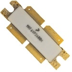
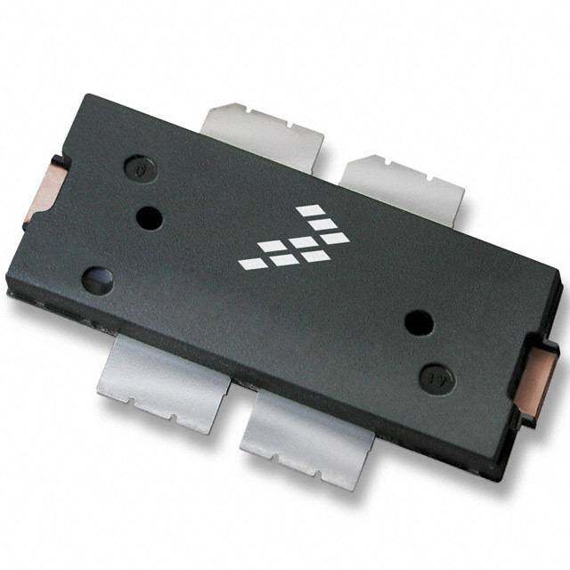
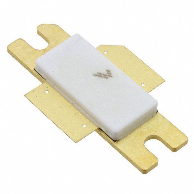
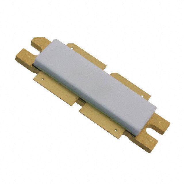
| 描述 | MOSFET RF N-CH 50V NI-1230射频MOSFET晶体管 VHV6 600W 225MHZ NI1230 |
| 产品分类 | RF FET分离式半导体 |
| 品牌 | Freescale Semiconductor |
| 产品手册 | |
| 产品图片 |
|
| rohs | 符合RoHS无铅 / 符合限制有害物质指令(RoHS)规范要求 |
| 产品系列 | 晶体管,晶体管射频,射频MOSFET晶体管,Freescale Semiconductor MRF6VP2600HR5- |
| 数据手册 | |
| 产品型号 | MRF6VP2600HR5 |
| Vds-Drain-SourceBreakdownVoltage | 110 V |
| Vds-漏源极击穿电压 | 110 V |
| Vgs-Gate-SourceBreakdownVoltage | 10 V |
| Vgs-栅源极击穿电压 | 10 V |
| Vgsth-Gate-SourceThresholdVoltage | 3 V |
| Vgsth-栅源极阈值电压 | 3 V |
| 产品目录页面 | |
| 产品种类 | 射频MOSFET晶体管 |
| 产品类型 | RF MOSFET Power |
| 供应商器件封装 | NI-1230 |
| 其它名称 | MRF6VP2600HR5TR |
| 功率-输出 | 125W |
| 包装 | 带卷 (TR) |
| 单位重量 | 13.155 g |
| 商标 | Freescale Semiconductor |
| 噪声系数 | - |
| 增益 | 25dB |
| 安装风格 | SMD/SMT |
| 封装 | Reel |
| 封装/外壳 | NI-1230 |
| 封装/箱体 | NI-1230 |
| 工厂包装数量 | 50 |
| 技术 | MOSFET |
| 晶体管极性 | N-Channel |
| 晶体管类型 | LDMOS(双) |
| 最大工作温度 | + 150 C |
| 标准包装 | 50 |
| 汲极/源极击穿电压 | 110 V |
| 电压-测试 | 50V |
| 电压-额定 | 110V |
| 电流-测试 | 2.6A |
| 系列 | MRF6VP2600H |
| 输出功率 | 600 W at Peak |
| 配置 | Dual |
| 闸/源击穿电压 | 10 V |
| 频率 | 225MHz |
| 额定电流 | 2.5mA |


- 商务部:美国ITC正式对集成电路等产品启动337调查
- 曝三星4nm工艺存在良率问题 高通将骁龙8 Gen1或转产台积电
- 太阳诱电将投资9.5亿元在常州建新厂生产MLCC 预计2023年完工
- 英特尔发布欧洲新工厂建设计划 深化IDM 2.0 战略
- 台积电先进制程称霸业界 有大客户加持明年业绩稳了
- 达到5530亿美元!SIA预计今年全球半导体销售额将创下新高
- 英特尔拟将自动驾驶子公司Mobileye上市 估值或超500亿美元
- 三星加码芯片和SET,合并消费电子和移动部门,撤换高东真等 CEO
- 三星电子宣布重大人事变动 还合并消费电子和移动部门
- 海关总署:前11个月进口集成电路产品价值2.52万亿元 增长14.8%

PDF Datasheet 数据手册内容提取
Freescale Semiconductor DocumentNumber:MRF6VP2600H Technical Data Rev.5.1,7/2010 RF Power Field Effect Transistor N--Channel Enhancement--Mode Lateral MOSFET MRF6VP2600HR6 Designedprimarilyforwidebandapplicationswithfrequenciesupto500MHz. Deviceisunmatchedandissuitableforuseinbroadcastapplications. • TypicalDVB--TOFDMPerformance:VDD=50Volts,IDQ=2600mA, Pout=125WattsAvg.,f=225MHz,ChannelBandwidth=7.61MHz, 2--500MHz,600W,50V InputSignalPAR=9.3dB@0.01%ProbabilityonCCDF. LATERALN--CHANNEL PowerGain(cid:151)25dB BROADBAND DrainEfficiency(cid:151)28.5% RFPOWERMOSFET ACPR@4MHzOffset(cid:151)--61dBc@4kHzBandwidth • TypicalPulsedPerformance:VDD=50Volts,IDQ=2600mA, Pout=600WattsPeak,f=225MHz,PulseWidth=100μsec,Duty Cycle=20% PowerGain(cid:151)25.3dB DrainEfficiency(cid:151)59% • CapableofHandling10:1VSWR,@50Vdc,225MHz,600WattsPeak Power,PulseWidth=100μsec,DutyCycle=20% Features • CharacterizedwithSeriesEquivalentLarge--SignalImpedanceParameters CASE375D--05,STYLE1 • CWOperationCapabilitywithAdequateCooling NI--1230 • QualifiedUptoaMaximumof50VDDOperation PARTISPUSH--PULL • IntegratedESDProtection • DesignedforPush--PullOperation • GreaterNegativeGate--SourceVoltageRangeforImprovedClassC Operation • RoHSCompliant • InTapeandReel.R6Suffix=150Unitsper56mm,13inchReel. RFinA/VGSA 3 1 RFoutA/VDSA RFinB/VGSB 4 2 RFoutB/VDSB (TopView) Figure1.PinConnections Table1.MaximumRatings Rating Symbol Value Unit Drain--SourceVoltage VDSS --0.5,+110 Vdc Gate--SourceVoltage VGS --6.0,+10 Vdc StorageTemperatureRange Tstg --65to+150 °C CaseOperatingTemperature TC 150 °C OperatingJunctionTemperature(1,2) TJ 225 °C Table2.ThermalCharacteristics Characteristic Symbol Value(2,3) Unit ThermalResistance,JunctiontoCase RθJC °C/W CaseTemperature99°C,125WCW,225MHz,50Vdc,IDQ=2600mA 0.20 CaseTemperature64°C,610WCW,352.2MHz,50Vdc,IDQ=150mA 0.14 CaseTemperature81°C,610WCW,88--108MHz,50Vdc,IDQ=150mA 0.16 1. ContinuoususeatmaximumtemperaturewillaffectMTTF. 2. MTTFcalculatoravailableathttp://www.freescale.com/rf.SelectSoftware&Tools/DevelopmentTools/CalculatorstoaccessMTTF calculatorsbyproduct. 3. RefertoAN1955,ThermalMeasurementMethodologyofRFPowerAmplifiers.Gotohttp://www.freescale.com/rf. SelectDocumentation/ApplicationNotes--AN1955. ©FreescaleSemiconductor,Inc.,2008--2010.Allrightsreserved. MRF6VP2600HR6 RFDeviceData FreescaleSemiconductor 1
Table3.ESDProtectionCharacteristics TestMethodology Class HumanBodyModel(perJESD22--A114) 2(Minimum) MachineModel(perEIA/JESD22--A115) A(Minimum) ChargeDeviceModel(perJESD22--C101) IV(Minimum) Table4.ElectricalCharacteristics (TA=25°Cunlessotherwisenoted) Characteristic Symbol Min Typ Max Unit OffCharacteristics(1) Gate--SourceLeakageCurrent IGSS (cid:151) (cid:151) 10 μAdc (VGS=5Vdc,VDS=0Vdc) Drain--SourceBreakdownVoltage V(BR)DSS 110 (cid:151) (cid:151) Vdc (ID=150mA,VGS=0Vdc) ZeroGateVoltageDrainLeakageCurrent IDSS (cid:151) (cid:151) 50 μAdc (VDS=50Vdc,VGS=0Vdc) ZeroGateVoltageDrainLeakageCurrent IDSS (cid:151) (cid:151) 2.5 mA (VDS=100Vdc,VGS=0Vdc) OnCharacteristics GateThresholdVoltage(1) VGS(th) 1 1.65 3 Vdc (VDS=10Vdc,ID=800μAdc) GateQuiescentVoltage(2) VGS(Q) 1.5 2.7 3.5 Vdc (VDD=50Vdc,ID=2600mAdc,MeasuredinFunctionalTest) Drain--SourceOn--Voltage(1) VDS(on) (cid:151) 0.25 (cid:151) Vdc (VGS=10Vdc,ID=2Adc) DynamicCharacteristics(1) ReverseTransferCapacitance Crss (cid:151) 1.7 (cid:151) pF (VDS=50Vdc±30mV(rms)ac@1MHz,VGS=0Vdc) OutputCapacitance Coss (cid:151) 101 (cid:151) pF (VDS=50Vdc±30mV(rms)ac@1MHz,VGS=0Vdc) InputCapacitance Ciss (cid:151) 287 (cid:151) pF (VDS=50Vdc,VGS=0Vdc±30mV(rms)ac@1MHz) FunctionalTests(2)(InFreescaleTestFixture,50ohmsystem)VDD=50Vdc,IDQ=2600mA,Pout=125WAvg.,f=225MHz,DVB--T OFDMSingleChannel.ACPRmeasuredin7.61MHzChannelBandwidth@±4MHzOffset. PowerGain Gps 24 25 27 dB DrainEfficiency ηD 27 28.5 (cid:151) % AdjacentChannelPowerRatio ACPR (cid:151) --61 --59 dBc InputReturnLoss IRL (cid:151) --18 --9 dB TypicalPerformance(cid:151)352.2MHz(InFreescale352.2MHzTestFixture,50ohmsystem)VDD=50Vdc,IDQ=150mA,Pout=600WCW PowerGain Gps (cid:151) 22 (cid:151) dB DrainEfficiency ηD (cid:151) 68 (cid:151) % InputReturnLoss IRL (cid:151) --15 (cid:151) dB TypicalPerformance(cid:151)88--108MHz(InFreescale88--108MHzTestFixture,50ohmsystem)VDD=50Vdc,IDQ=150mA,Pout=600W CW PowerGain Gps (cid:151) 24.5 (cid:151) dB DrainEfficiency ηD (cid:151) 74 (cid:151) % InputReturnLoss IRL (cid:151) --5 (cid:151) dB 1. Eachsideofdevicemeasuredseparately. 2. Measurementmadewithdeviceinpush--pullconfiguration. MRF6VP2600HR6 RFDeviceData 2 FreescaleSemiconductor
R1 VBIAS B1 L3 L2 VSUPPLY + + + L4 + + + C16 C15 C14 C13 C12 C11 C9 C8 C7 C10 C6 C19 C17 C18 C20 C21 C22 C23 C24 C25 Z9 Z11 Z13 Z15 Z17 Z5 Z7 RF RF INPUT OUTPUT Z1 Z2 L1 Z3 Z4 Z19 Z20 DUT C3 C4 J1 J2 Z6 Z8 C1 C2 Z10 Z12 Z14 Z16 Z18 C5 T1 T2 Z1 1.049″x0.080″Microstrip Z13,Z14 0.224″x0.253″Microstrip Z2* 0.143″x0.080″Microstrip Z15*,Z16* 0.095″x0.253″Microstrip Z3* 0.188″x0.080″Microstrip Z17,Z18 0.052″x0.253″Microstrip Z4 0.192″x0.133″Microstrip Z19 0.053″x0.080″Microstrip Z5,Z6 0.418″x0.193″Microstrip Z20 1.062″x0.080″Microstrip Z7,Z8 0.217″x0.518″Microstrip PCB ArlonCuClad250GX--0300--55--22,0.030″,εr=2.55 Z9,Z10 0.200″x0.518″Microstrip *Linelengthincludesmicrostripbends Z11,Z12 0.375″x0.214″Microstrip Figure2.MRF6VP2600HR6TestCircuitSchematic Table5.MRF6VP2600HR6TestCircuitComponentDesignationsandValues Part Description PartNumber Manufacturer B1 95Ω,100MHzLongFerriteBead 2743021447 Fair--Rite C1 47pFChipCapacitor ATC100B470JT500XT ATC C2,C4 43pFChipCapacitors ATC100B430JT500XT ATC C3 100pFChipCapacitor ATC100B101JT500XT ATC C5 10pFChipCapacitor ATC100B7R5CT500XT ATC C6,C9 2.2μF,50VChipCapacitors C1825C225J5RAC Kemet C7,C13,C20 10KpFChipCapacitors ATC200B103KT50XT ATC C8 220nF,50VChipCapacitor C1812C224J5RAC Kemet C10,C17,C18 1000pFChipCapacitors ATC100B102JT50XT ATC C11,C22 0.1μF,50VChipCapacitors CDR33BX104AKYS Kemet C12,C21 20KpFChipCapacitors ATC200B203KT50XT ATC C14 10μF,35VTantalumCapacitor T491D106K035AT Kemet C15 22μF,35VTantalumCapacitor T491X226K035AT Kemet C16 47μF,50VElectrolyticCapacitor 476KXM050M IllinoisCap C19 2.2μF,ChipCapacitor 2225X7R225KT3AB ATC C23,C24,C25 470μF63VElectrolyticCapacitors MCGPR63V477M13X26--RH Multicomp J1,J2 JumpersfromPCBtoT1&T2 CopperFoil L1 17.5nH,6TurnInductor B06T CoilCraft L2 8Turn,#20AWGID=0.125″Inductor,HandWound CopperWire L3 82nH,Inductor 1812SMS--82NJ CoilCraft L4* 9Turn,#18AWGInductor,HandWound CopperWire R1 20Ω,3WAxialLeadedResistor 5093NW20R00J Vishay T1 Balun TUI--9 CommConcepts T2 Balun TUO--4 CommConcepts *L4iswrappedaroundR1. MRF6VP2600HR6 RFDeviceData FreescaleSemiconductor 3
-- B1 C23 C13 C16 C22 C12 + C21 C11 C20 C24 C25 -- L4,R1* -- C15 L3 C14 C9 C18 C19 C8 L2 C17 C7 C10 T2 C6 T1 J1 C4 J2 A E R A C1 L1 C2 UT C5 O T U C C3(onside) MRF6VP2600H 225MHz Rev.3 *L4iswrappedaroundR1. Figure3.MRF6VP2600HR6TestCircuitComponentLayout MRF6VP2600HR6 RFDeviceData 4 FreescaleSemiconductor
TYPICALCHARACTERISTICS 1000 100 Ciss pF) 100 Coss AMPS) TJ=200_C NCE( ENT( TJ=150_C TJ=175_C TA Measuredwith±30mV(rms)ac@1MHz RR 10 ACI VGS=0Vdc CU CAP 10 Crss AIN C, DR ,D I TC=25_C 1 1 0 10 20 30 40 50 1 10 100 VDS,DRAIN--SOURCEVOLTAGE(VOLTS) VDS,DRAIN--SOURCEVOLTAGE(VOLTS) Note:Eachsideofdevicemeasuredseparately. Note:Eachsideofdevicemeasuredseparately. Figure4.CapacitanceversusDrain--SourceVoltage Figure5.DCSafeOperatingArea 26.5 80 64 Gps P3dB=59.7dBm(938W) Ideal 26 70 62 25.5 60 %) m) P2dB=59.1dBm(827W) G,POWERGAIN(dB)ps2243222..55543 VfPD=DuulDt2sye2=C5W5yM0cidlHeVthzd=c=2,10ID0%Q0μ=s2e6c00mA ηD 5432100000 DRAINEFFICIENCY(ηD, P,OUTPUTPOWER(dBout 56558064 P1dB=53.3dBm(670VDWD)=50Vdc,IDQ=2600mA,f=225AcMtuHazl PulseWidth=12μsec,DutyCycle=1% 22.5 0 52 10 100 1000 27 28 29 30 31 32 33 34 35 36 37 38 Pout,OUTPUTPOWER(WATTS)PULSED Pin,INPUTPOWER(dBm) Figure6.PulsedPowerGainandDrainEfficiency Figure7.PulsedCWOutputPowerversus versusOutputPower InputPower 26 28 80 27 Gps 70 25 TC=--30_C AIN(dB) 24 50V AIN(dB) 2256 25_C 5600 ENCY(%) RG 45V RG 85_C FICI WE 40V WE 24 40 EF G,POps 2232 VIfD=DQD2=2=5256M00H0VzdmcA 35V G,POps 23 VfP=DulD2se2=5W5M0idHVthzdc=,1ID0Q0μ=s2e6c00mA ηD 30 DRAINηD, PulseWidth=100μsec 22 DutyCycle=20% 20 DutyCycle=20% VDD=30V 21 21 10 0 100 200 300 400 500 600 700 10 100 1000 Pout,OUTPUTPOWER(WATTS)PULSED Pout,OUTPUTPOWER(WATTS)PULSED Figure8.PulsedPowerGainversus Figure9.PulsedPowerGainandDrainEfficiency OutputPower versusOutputPower MRF6VP2600HR6 RFDeviceData FreescaleSemiconductor 5
TYPICALCHARACTERISTICS(cid:151)TWO--TONE --20 --10 Bc) VDD=50Vdc,IDQ=2600mA,f1=222MHz Bc) VDD=50Vdc,Pout=500W(PEP),IDQ=2600mA (d f2=228MHz,Two--ToneMeasurements (d Two--ToneMeasurements ON --30 ON --20 TI TI R R O O T T DIS --40 DIS --30 3rdOrder N 3rdOrder N O O TI TI LA --50 LA --40 5thOrder U U D D O 5thOrder O M M ER --60 ER --50 7thOrder T T N 7thOrder N I I D, D, M M I --70 I --60 5 10 100 700 0.1 1 10 40 Pout,OUTPUTPOWER(WATTS)PEP TWO--TONESPACING(MHz) Figure10.IntermodulationDistortion Figure11.IntermodulationDistortion ProductsversusOutputPower ProductsversusToneSpacing 26 --20 VDD=50Vdc,f1=222MHz,f2=228MHz IDQ=2600mA dBc) --25 Two--ToneMeasurements,6MHzToneSpacing 25.5 ( N ERGAIN(dB) 25 22030000mmAA RDORDERNDISTORTIO ----3305 IDQ=1300mA G,POWps24.5 1800mA IMD,THIODULATIO --40 18002m60A0mA M 24 1300mA VDD=50Vdc,f1=222MHz,f2=228MHz NTER --45 2000mA Two--ToneMeasurements,6MHzToneSpacing I 2300mA 23.5 --50 20 100 700 20 100 700 Pout,OUTPUTPOWER(WATTS)PEP Pout,OUTPUTPOWER(WATTS)PEP Figure12.Two--TonePowerGainversus Figure13.ThirdOrderIntermodulation OutputPower DistortionversusOutputPower MRF6VP2600HR6 RFDeviceData 6 FreescaleSemiconductor
TYPICALCHARACTERISTICS(cid:151)OFDM 100 --20 7.61MHz 10 --30 --40 %) 1 --50 4kHzBW 4kHzBW ( Y T --60 ABILI 0.1 8KModeDVB--TOFDM dB) --70 ACPRMeasuredat4MHzOffset B ( fromCenterFrequency O 64QAMDataCarrierModulation R 0.01 --80 P 5Symbols --90 8KModeDVB--TOFDM 0.001 --100 64QAMDataCarrierModulation,5Symbols --110 0.0001 0 2 4 6 8 10 12 --5 --4 --3 --2 --1 0 1 2 3 4 5 PEAK--TO--AVERAGE(dB) f,FREQUENCY(MHz) Figure14.Single--CarrierDVB--TOFDM Figure15.8KModeDVB--TOFDMSpectrum 25.8 c) --56 B 25.6 IDQ=2600mA ATIO(d --58 V8KDDM=od5e0OVdFcD,Mf=,6242Q5AMMHzDataCarrier R Modulation,5Symbols B)25.4 2300mA ER N(d25.2 2000mA OW --60 AI P G L E R 25 N --62 E N OW 1800mA HA IDQ=1300mA P24.8 C G,ps24.6 1300mA VDD=50Vdc,f=225MHz DJACENT ----6646 1800mA 24.4 8KModeOFDM,64QAMDataCarrier A 2000mA Modulation,5Symbols PR, 2300mA 2600mA 24.2 C --68 A 30 100 200 20 100 200 Pout,OUTPUTPOWER(WATTS)AVG. Pout,OUTPUTPOWER(WATTS)AVG. Figure16.Single--CarrierDVB--TOFDMPower Figure17.Single--CarrierDVB--TOFDMACPR GainversusOutputPower versusOutputPower B) 45 --56 Bc) (d 25_C --30_C (d N O GAI 40 85_C --58 ATI R R E R W ACPR E O 35 --60 W P O G,ps ηD ELP NCY(%), 3205 25_C TC=--30_C Gps ----6624 TCHANN FICIE 85_C VDD=50Vdc,IDQ=2600MHz ACEN EF 20 f=225MHz,8KModeOFDM --66 DJ N 64QAMDataCarrierModulation A AI R, R 5Symbols P D 15 --68 C ,ηD 30 100 400 A Pout,OUTPUTPOWER(WATTS)AVG. Figure18.Single--CarrierDVB--TOFDMACPRPower GainandDrainEfficiencyversusOutputPower MRF6VP2600HR6 RFDeviceData FreescaleSemiconductor 7
TYPICALCHARACTERISTICS 109 108 S) R U O 107 H ( F T T M 106 105 90 110 130 150 170 190 210 230 250 TJ,JUNCTIONTEMPERATURE(°C) ThisabovegraphdisplayscalculatedMTTFinhourswhenthedevice isoperatedatVDD=50Vdc,Pout=125WAvg.,andηD=28.5%. MTTFcalculatoravailableathttp://www.freescale.com/rf.Select Software&Tools/DevelopmentTools/CalculatorstoaccessMTTF calculatorsbyproduct. Figure19.MTTFversusJunctionTemperature-- CW MRF6VP2600HR6 RFDeviceData 8 FreescaleSemiconductor
Zsource f=225MHz Zo=10Ω Zload f=225MHz VDD=50Vdc,IDQ=2600mA,Pout=125WAvg. f Zsource Zload MHz Ω Ω 225 1.42+j8.09 4.45+j1.16 Zsource = Testcircuitimpedanceasmeasuredfrom gatetogate,balancedconfiguration. Zload = Testcircuitimpedanceasmeasuredfrom draintodrain,balancedconfiguration. Input Device Output Matching + Under -- Matching Network Test Network -- + Z Z source load Figure20.SeriesEquivalentSourceandLoadImpedance MRF6VP2600HR6 RFDeviceData FreescaleSemiconductor 9
COAX1 C18 C16 C17 + C15 C14 + + C1 J1 C3 B1 C5 R1 C7 C4 L3 C8 C9 A E L1 T1 R A C10 T U L4 O L2 T C2 U C6 C C11 C12 COAX3 MRF6VP2600KHRev.2 C13 88--108MHz COAX2 Figure21.MRF6VP2600HR6TestCircuitComponentLayout(cid:151)88--108MHz Table6.MRF6VP2600HR6TestCircuitComponentDesignationsandValues(cid:151)88--108MHz Part Description PartNumber Manufacturer B1 95Ω,100MHzLongFerriteBead 2743021447 Fair--Rite C1 6.8μF,50VChipCapacitor C4532X7R1H685K TDK C2 30pFChipCapacitor ATC100B300JT500XT ATC C3,C13,C14 1000pFChipCapacitors ATC100B102JT50XT ATC C4,C5,C6 1μF,100VChipCapacitors GRM31CR72A105KA01L Murata C7,C8,C9,C10, 3900pFChipCapacitors ATC700B392JT50X ATC C11,C12 C15 4.7μF,100VChipCapacitor GRM55ER72A475KA01B Murata C16,C17 470μF,63VElectrolyticCapacitors MCGPR63V477M13X26--RH Multicomp C18 220μF,100VElectrolyticCapacitor MCGPR100V227M16X26--RH Multicomp J1 JumperwithCopperTape L1 82nHInductor 1812SMS--82NJ CoilCraft L2 8Turn,#14AWGID=0.250″Inductor,HandWound CopperWire Freescale L3,L4 8nHInductors A03TKLC CoilCraft R1 15Ω,1/4WChipResistor CRCW120615R0FKEA Vishay T1 BalunTransformer TUI--LF--9 CommConcepts Coax1,Coax2 25Ω,SemiRigidRFCable,3mmLine,16cmLength UT--141C--25 Micro--Coax Coax3 25Ω,SemiRigidRFCable,3mmLine,15cmLength UT--141C--25 Micro--Coax PCB 0.030″,εr=2.55 GX0300--55--22 Arlon MRF6VP2600HR6 RFDeviceData 10 FreescaleSemiconductor
TYPICALCHARACTERISTICS(cid:151)88--108MHz 30 85 29 VDD=50Vdc,IDQ=150mA 108MHz 80 28 75 AIN(dB) 2267 98MHz108MHz Gps 88M98HMzHz 6750 ENCY(%) G CI WER 25 88MHz 60 EFFI O 24 55 N P AI G,ps 23 ηD 50 DR,D 22 45 η 21 40 20 35 100 200 300 400 500 600 700800 Pout,OUTPUTPOWER(WATTS) Figure22.BroadbandCWPowerGainandDrain EfficiencyversusOutputPower(cid:151)88--108MHz 27 82 26.5 VDD=50Vdc,IDQ=150mA 81 Pout=600W,CW 26 80 %) dB) 25.5 Gps 79 CY( N( 25 78 EN AI CI G 24.5 77 FI R F E E W 24 76 N O AI G,Pps 23.5 ηD 75 ,DRD 23 74 η 22.5 73 22 72 86 90 94 98 102 106 110 f,FREQUENCY(MHz) Figure23.CWPowerGainandDrainEfficiency versusFrequency(cid:151)88--108MHz MRF6VP2600HR6 RFDeviceData FreescaleSemiconductor 11
f=88MHz f=108MHz Zsource Zo=25Ω Zload f=108MHz f=88MHz VDD=50Vdc,IDQ=150mA,Pout=600WAvg. f Zsource Zload MHz Ω Ω 88 3.20+j14.50 10.35+j2.80 98 4.20+j15.00 9.50+j3.00 108 4.00+j15.00 8.90+j3.50 Zsource = Testcircuitimpedanceasmeasuredfrom gatetogate,balancedconfiguration. Zload = Testcircuitimpedanceasmeasuredfrom draintodrain,balancedconfiguration. Input Device Output Matching + Under -- Matching Network Test Network -- + Z Z source load Figure24.SeriesEquivalentSourceandLoadImpedance(cid:151)88--108MHz MRF6VP2600HR6 RFDeviceData 12 FreescaleSemiconductor
-- -- C11 C9 C20 C22 MRF6VP2600H B1 C7 352.2MHz C5 Rev.1 L3 C18 COAX1 L1 COAX3 C14 C1 C3* C13 C15 C2 C4* EA C16 C24* R C17 A T U O T U COAX2 L2 C COAX4 C19 L4 C6 B2 C10 -- -- C21 C23 C8 C12 *Mountedonside Figure25.MRF6VP2600HR6TestCircuitComponentLayout(cid:151)352.2MHz Table7.MRF6VP2600HR6TestCircuitComponentDesignationsandValues(cid:151)352.2MHz Part Description PartNumber Manufacturer B1,B2 47Ω,100MHzShortFerriteBeads 2743019447 Fair--Rite C1,C2 100pFChipCapacitors ATC100B101JT500XT ATC C3*,C24* 22pFChipCapacitors ATC100B221JT300XT ATC C4* 20pFChipCapacitor ATC100B200JT500XT ATC C5,C6 2.2μFChipCapacitors C1825C225J5RAC--TU Kemet C7,C8 220nFChipCapacitors C1812C224K5RAC--TU Kemet C9,C10 0.1μFChipCapacitors CDR33BX104AKWS AVX C11,C12 47μF,50VElectrolyticCapacitors 476KXM050M IllinoisCap C13 39pF,500VChipCapacitor MCM01--009DD390J--F CDE C14,C15,C16, 240pFChipCapacitors ATC100B241JT200XT ATC C17 C18,C19 2.2μFChipCapacitors G2225X7R225KT3AB ATC C20,C21,C22, 470μF,63VElectrolyticCapacitors MCGPR63V477M13X26--RH Multicomp C23 Coax1,2,3,4 25Ω,SemiRigidCoax,2.2″ UT141--25 PrecisionTubeCompany L1,L2 2.5nH,1TurnInductors A01TKLC Coilcraft L3,L4 10Turn,#16AWGID=0.160″Inductors,HandWound CopperWire Freescale *Mountedonside MRF6VP2600HR6 RFDeviceData FreescaleSemiconductor 13
TYPICALCHARACTERISTICS(cid:151)352.2MHz 23 80 Gps 22 VDD=50Vdc 70 IDQ=150mA 21 f=352.2MHz 60 %) N(dB) 20 50 NCY( GAI ηD CIE WER 19 40 EFFI PO 18 30 AIN G,ps 17 20 DRD, η 16 10 15 0 10 100 1000 Pout,OUTPUTPOWER(WATTS)CW Figure26.CWPowerGainandDrainEfficiency versusOutputPower MRF6VP2600HR6 RFDeviceData 14 FreescaleSemiconductor
Zo=10Ω f=352.2MHz Zsource f=352.2MHz Zload VDD=50Vdc,IDQ=150mA,Pout=600WCW f Zsource Zload MHz Ω Ω 352.2 1.10+j3.80 2.26+j3.57 Zsource = Testcircuitimpedanceasmeasuredfrom gatetogate,balancedconfiguration. Zload = Testcircuitimpedanceasmeasuredfrom draintodrain,balancedconfiguration. Input Device Output Matching + Under -- Matching Network Test Network -- + Z Z source load Figure27.SeriesEquivalentSourceandLoadImpedance(cid:151)352.2MHz MRF6VP2600HR6 RFDeviceData FreescaleSemiconductor 15
PACKAGEDIMENSIONS MRF6VP2600HR6 RFDeviceData 16 FreescaleSemiconductor
MRF6VP2600HR6 RFDeviceData FreescaleSemiconductor 17
PRODUCTDOCUMENTATIONANDSOFTWARE Refertothefollowingdocumentstoaidyourdesignprocess. ApplicationNotes • AN1955:ThermalMeasurementMethodologyofRFPowerAmplifiers EngineeringBulletins • EB212:UsingDataSheetImpedancesforRFLDMOSDevices Software • ElectromigrationMTTFCalculator • RFHighPowerModel ForSoftware,doaPartNumbersearchathttp://www.freescale.com,andselectthe(cid:147)PartNumber(cid:148)link.GototheSoftware& Toolstabonthepart(cid:146)sProductSummarypagetodownloadtherespectivetool. REVISIONHISTORY Thefollowingtablesummarizesrevisionstothisdocument. Revision Date Description 0 Mar.2008 • InitialReleaseofDataSheet 1 July2008 • RemovedCapableofHandling5:1VSWRbullet,p.1 • CorrectedZsourceandZloadvaluesfrom1.58+j6.47to1.42+j8.09and4.60+j1.85to4.45+j1.16andre- plotteddatainFig.21,SeriesEquivalentSourceandLoadImpedance,p.9 2 Sept.2008 • AddedNotetoFig.4,CapacitanceversusDrain--SourceVoltageandFig.5,DCSafeOperatingAreatode- notethateachsideofdeviceismeasuredseparately,p.5 • UpdatedFig.5,DCSafeOperatingArea,toshowonesideofthedevice,p.5 • Figs.21and27,SeriesEquivalentSourceandLoadImpedance,correctedZsourcecopytoread(cid:147)Testcircuit impedanceasmeasuredfromgatetogate,balancedconfiguration(cid:148)andZloadcopytoread(cid:147)Testcircuit impedanceasmeasuredfromgatetogate,balancedconfiguration(cid:148),p.9,14 2.1 Nov.2008 • CorrectedFigs.21and27RevisionHistoryZloadcopytoread(cid:148)Testcircuitimpedanceasmeasuredfrom draintodrain,balancedconfiguration(cid:148),p.9,14 4 May2009 • UpdatedbulletsinFeaturessectiontoreflectconsistentlistingacrossproducts,p.1 • Addedthermaldatafor352.2MHzapplicationtoTable2,ThermalCharacteristics,p.1 • AddedTypicalPerformancestablefor352.2MHzapplication,p.2 • AddedFig.28,TestCircuitComponentLayout--352.2MHzandTable7,TestCircuitComponentDesignations andValues--352.2MHz,p.15 • AddedFig.29,CWPowerGainandDrainEfficiencyversusOutputPower--352.2MHzp.16 • AddedFig.30,SeriesEquivalentSourceandLoadImpedance--352.2MHz,p.17 4.1 June2009 • Changed(cid:147)EKME630ELL471MK25S(cid:148)partnumberto(cid:147)MCGPR63V477M13X26--RH(cid:148),Table5,TestCircuit ComponentDesignationsandValuesandTable6,TestCircuitComponentDesignationsandValues(cid:151) 88--108MHz,p.3,11 • AddedElectromigrationMTTFCalculatorandRFHighPowerModelavailabilitytoProductDocumentation, ToolsandSoftware,p.20 5 May2010 • Changed10--500MHzto2--500MHzinDeviceDescriptionbox,p.1 • OperatingJunctionTemperatureincreasedfrom200°Cto225°CinMaximumRatingstableandrelated (cid:147)ContinuoususeatmaximumtemperaturewillaffectMTTF(cid:148)footnoteadded,p.1 • Addedthermaldatafor88--108MHzapplicationtoThermalCharacteristicstable,p.1 • AddedTypicalPerformancetablefor88--108MHzapplication,p.2 • RemovedFig.20,MTTFversusJunctionTemperature--Pulsedandrenumberedaccordingly,p.8 • ReplacedFig.22TestCircuitComponentLayout,Table6.TestCircuitComponentDesignationsandValues, theTypicalCharacteristiccurvesandFig.27SeriesImpedancefor88--108MHzwithimprovedcircuit performancefigures.The88--108MHzapplicationcircuitisalsonowamorecompactsize.,p.10--12 5.1 July2010 • Fig.24,SeriesImpedancefor88--108MHz,tableandplotupdatedtoreflectcorrectlocationofZsourceand Zload,p.12 MRF6VP2600HR6 RFDeviceData 18 FreescaleSemiconductor
HowtoReachUs: HomePage: www.freescale.com WebSupport: http://www.freescale.com/support USA/EuropeorLocationsNotListed: FreescaleSemiconductor,Inc. TechnicalInformationCenter,EL516 2100EastElliotRoad Tempe,Arizona85284 1--800--521--6274or+1--480--768--2130 www.freescale.com/support Europe,MiddleEast,andAfrica: FreescaleHalbleiterDeutschlandGmbH Informationinthisdocumentisprovidedsolelytoenablesystemandsoftware TechnicalInformationCenter implementerstouseFreescaleSemiconductorproducts.Therearenoexpressor Schatzbogen7 81829Muenchen,Germany impliedcopyrightlicensesgrantedhereundertodesignorfabricateanyintegrated +441296380456(English) circuitsorintegratedcircuitsbasedontheinformationinthisdocument. +46852200080(English) +498992103559(German) FreescaleSemiconductorreservestherighttomakechangeswithoutfurthernoticeto +33169354848(French) anyproductsherein.FreescaleSemiconductormakesnowarranty,representationor www.freescale.com/support guaranteeregardingthesuitabilityofitsproductsforanyparticularpurpose,nordoes FreescaleSemiconductorassumeanyliabilityarisingoutoftheapplicationoruseof Japan: anyproductorcircuit,andspecificallydisclaimsanyandallliability,includingwithout FreescaleSemiconductorJapanLtd. Headquarters limitationconsequentialorincidentaldamages.(cid:147)Typical(cid:148)parametersthatmaybe ARCOTower15F providedinFreescaleSemiconductordatasheetsand/orspecificationscananddo 1--8--1,Shimo--Meguro,Meguro--ku, varyindifferentapplicationsandactualperformancemayvaryovertime.Alloperating Tokyo153--0064 parameters,including(cid:147)Typicals(cid:148),mustbevalidatedforeachcustomerapplicationby Japan customer(cid:146)stechnicalexperts.FreescaleSemiconductordoesnotconveyanylicense 0120191014or+81354379125 underitspatentrightsnortherightsofothers.FreescaleSemiconductorproductsare support.japan@freescale.com notdesigned,intended,orauthorizedforuseascomponentsinsystemsintendedfor surgicalimplantintothebody,orotherapplicationsintendedtosupportorsustainlife, Asia/Pacific: FreescaleSemiconductorChinaLtd. orforanyotherapplicationinwhichthefailureoftheFreescaleSemiconductorproduct ExchangeBuilding23F couldcreateasituationwherepersonalinjuryordeathmayoccur.ShouldBuyer No.118JianguoRoad purchaseoruseFreescaleSemiconductorproductsforanysuchunintendedor ChaoyangDistrict unauthorizedapplication,BuyershallindemnifyandholdFreescaleSemiconductor Beijing100022 anditsofficers,employees,subsidiaries,affiliates,anddistributorsharmlessagainstall China claims,costs,damages,andexpenses,andreasonableattorneyfeesarisingoutof, +861058798000 directlyorindirectly,anyclaimofpersonalinjuryordeathassociatedwithsuch support.asia@freescale.com unintendedorunauthorizeduse,evenifsuchclaimallegesthatFreescale Semiconductorwasnegligentregardingthedesignormanufactureofthepart. ForLiteratureRequestsOnly: FreescaleSemiconductorLiteratureDistributionCenter 1--800--441--2447or+1--303--675--2140 FreescaletandtheFreescalelogoaretrademarksofFreescaleSemiconductor,Inc. Fax:+1--303--675--2150 Allotherproductorservicenamesarethepropertyoftheirrespectiveowners. LDCForFreescaleSemiconductor@hibbertgroup.com ©FreescaleSemiconductor,Inc.2008--2010.Allrightsreserved. MRF6VP2600HR6 RDFocDumeevnicteNuDmabetar:MRF6VP2600H FRreeve.s5.c1a,7le/20S10emiconductor 19
Mouser Electronics Authorized Distributor Click to View Pricing, Inventory, Delivery & Lifecycle Information: N XP: MRF6VP2600HR6 MRF6VP2600HR5