ICGOO在线商城 > 分立半导体产品 > 晶体管 - FET,MOSFET - 射频 > MRF6V2010NR1
 Datasheet下载
- 型号: MRF6V2010NR1
- 制造商: Freescale Semiconductor
- 库位|库存: xxxx|xxxx
- 要求:
| 数量阶梯 | 香港交货 | 国内含税 |
| +xxxx | $xxxx | ¥xxxx |
查看当月历史价格
查看今年历史价格
MRF6V2010NR1产品简介:
ICGOO电子元器件商城为您提供MRF6V2010NR1由Freescale Semiconductor设计生产,在icgoo商城现货销售,并且可以通过原厂、代理商等渠道进行代购。 MRF6V2010NR1价格参考。Freescale SemiconductorMRF6V2010NR1封装/规格:晶体管 - FET,MOSFET - 射频, 射频 Mosfet LDMOS 50V 30mA 220MHz 23.9dB 10W TO-270-2。您可以下载MRF6V2010NR1参考资料、Datasheet数据手册功能说明书,资料中有MRF6V2010NR1 详细功能的应用电路图电压和使用方法及教程。
| 参数 | 数值 |
| 产品目录 | |
| 描述 | IC MOSFET RF N-CHAN TO270-2 |
| 产品分类 | RF FET |
| 品牌 | Freescale Semiconductor |
| 数据手册 | |
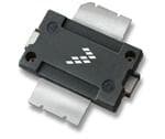
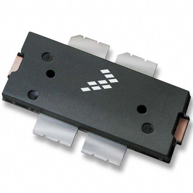
| 产品图片 |
|
| 产品型号 | MRF6V2010NR1 |
| rohs | 含铅 / 符合限制有害物质指令(RoHS)规范要求 |
| 产品系列 | - |
| 供应商器件封装 | TO-270-2 |
| 其它名称 | MRF6V2010NR1DKR |
| 功率-输出 | 10W |
| 包装 | Digi-Reel® |
| 噪声系数 | - |
| 增益 | 23.9dB |
| 封装/外壳 | TO-270AA |
| 晶体管类型 | LDMOS |
| 标准包装 | 1 |
| 电压-测试 | 50V |
| 电压-额定 | 110V |
| 电流-测试 | 30mA |
| 频率 | 220MHz |
| 额定电流 | 2.5mA |


- 商务部:美国ITC正式对集成电路等产品启动337调查
- 曝三星4nm工艺存在良率问题 高通将骁龙8 Gen1或转产台积电
- 太阳诱电将投资9.5亿元在常州建新厂生产MLCC 预计2023年完工
- 英特尔发布欧洲新工厂建设计划 深化IDM 2.0 战略
- 台积电先进制程称霸业界 有大客户加持明年业绩稳了
- 达到5530亿美元!SIA预计今年全球半导体销售额将创下新高
- 英特尔拟将自动驾驶子公司Mobileye上市 估值或超500亿美元
- 三星加码芯片和SET,合并消费电子和移动部门,撤换高东真等 CEO
- 三星电子宣布重大人事变动 还合并消费电子和移动部门
- 海关总署:前11个月进口集成电路产品价值2.52万亿元 增长14.8%


PDF Datasheet 数据手册内容提取
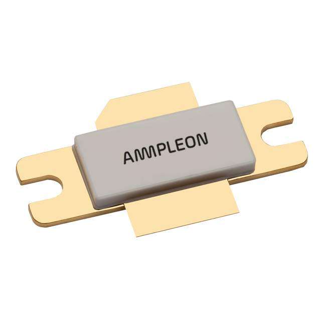
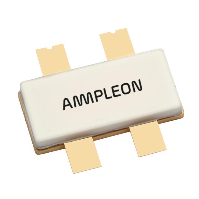
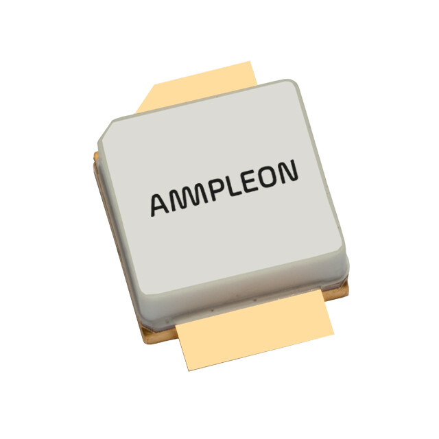
NXP Semiconductors DocumentNumber:MRF6V2010N Technical Data Rev.6,9/2016 RF Power Field Effect Transistors MRF6V2010N N--Channel Enhancement--Mode Lateral MOSFETs MRF6V2010NB DesignedprimarilyforCWlarge--signaloutputanddriverapplicationswith MRF6V2010GN frequenciesupto450MHz.Devicesareunmatchedandaresuitableforusein industrial,medicalandscientificapplications. TypicalCWperformanceat220MHz:VDD=50Vdc,IDQ=30mA, 10--450MHz,10W,50V P =10W out LATERALN--CHANNEL Powergain—23.9dB BROADBAND Drainefficiency—62% RFPOWERMOSFETs Capableofhandling10:1VSWR@50Vdc,220MHz,10WCW outputpower Features Characterizedwithseriesequivalentlarge--signalimpedanceparameters TO--270--2 PLASTIC Qualifieduptoamaximumof50VDDoperation MRF6V2010N IntegratedESDprotection 225Ccapableplasticpackage TO--272--2 PLASTIC MRF6V2010NB TO--270G--2 PLASTIC MRF6V2010GN Gate 2 1 Drain (TopView) Note: Exposedbacksideofthepackageis thesourceterminalforthetransistor. Figure1.PinConnections 2007–2008,2010,2016NXPB.V. MRF6V2010NMRF6V2010NBMRF6V2010GN RFDeviceData NXPSemiconductors 1
Table1.MaximumRatings Rating Symbol Value Unit Drain--SourceVoltage VDSS --0.5,+110 Vdc Gate--SourceVoltage VGS --0.5,+10 Vdc StorageTemperatureRange Tstg --65to+150 C CaseOperatingTemperature TC 150 C OperatingJunctionTemperature(1,2) TJ 225 C Table2.ThermalCharacteristics Characteristic Symbol Value(2,3) Unit ThermalResistance,JunctiontoCase CaseTemperature81C,10WCW RJC 3.0 C/W Table3.ESDProtectionCharacteristics TestMethodology Class HumanBodyModel(perJESD22--A114) 2 MachineModel(perEIA/JESD22--A115) A ChargeDeviceModel(perJESD22--C101) IV Table4.MoistureSensitivityLevel TestMethodology Rating PackagePeakTemperature Unit PerJESD22--A113,IPC/JEDECJ--STD--020 3 260 C Table5.ElectricalCharacteristics (TA=25Cunlessotherwisenoted) Characteristic Symbol Min Typ Max Unit OffCharacteristics Gate--SourceLeakageCurrent IGSS — — 10 Adc (VGS=5Vdc,VDS=0Vdc) Drain--SourceBreakdownVoltage V(BR)DSS 110 — — Vdc (ID=5mA,VGS=0Vdc) ZeroGateVoltageDrainLeakageCurrent IDSS — — 50 Adc (VDS=50Vdc,VGS=0Vdc) ZeroGateVoltageDrainLeakageCurrent IDSS — — 2.5 mA (VDS=100Vdc,VGS=0Vdc) OnCharacteristics GateThresholdVoltage VGS(th) 1 1.68 3 Vdc (VDS=10Vdc,ID=28Adc) GateQuiescentVoltage VGS(Q) 1.5 2.68 3.5 Vdc (VDD=50Vdc,ID=30mAdc,MeasuredinFunctionalTest) Drain--SourceOn--Voltage VDS(on) — 0.26 — Vdc (VGS=10Vdc,ID=70mAdc) DynamicCharacteristics ReverseTransferCapacitance Crss — 0.13 — pF (VDS=50Vdc30mV(rms)ac@1MHz,VGS=0Vdc) OutputCapacitance Coss — 7.3 — pF (VDS=50Vdc30mV(rms)ac@1MHz,VGS=0Vdc) InputCapacitance Ciss — 16.3 — pF (VDS=50Vdc,VGS=0Vdc30mV(rms)ac@1MHz) 1. ContinuoususeatmaximumtemperaturewillaffectMTTF. 2. MTTFcalculatoravailableathttp://www.nxp.com/RF/calculators. 3. RefertoAN1955,ThermalMeasurementMethodologyofRFPowerAmplifiers.Gotohttp://www.nxp.com/RFandsearchforAN1955. (continued) MRF6V2010NMRF6V2010NBMRF6V2010GN RFDeviceData 2 NXPSemiconductors
Table5.ElectricalCharacteristics (TA=25Cunlessotherwisenoted)(continued) Characteristic Symbol Min Typ Max Unit FunctionalTests(InNXPTestFixture,50ohmsystem)VDD=50Vdc,IDQ=30mA,Pout=10W,f=220MHz,CW PowerGain Gps 22.5 23.9 25.5 dB DrainEfficiency D 58 62 — % InputReturnLoss IRL — --14 --9 dB Table6.OrderingInformation Device TapeandReelInformation Package MRF6V2010NR1 R1Suffix=500Units,24mmTapeWidth,13--inchReel TO--270--2 MRF6V2010NBR1 R1Suffix=500Units,44mmTapeWidth,13--inchReel TO--272--2 MRF6V2010GNR1 R1Suffix=500Units,24mmTapeWidth,13--inchReel TO--270G--2 ATTENTION:TheMRF6V2010N,MRF6V2010NBandMRF6V2010GNarehighpowerdevicesandspecial considerationsmustbefollowedinboarddesignandmounting.Incorrectmountingcanleadtointernal temperatureswhichexceedthemaximumallowableoperatingjunctiontemperature.RefertoNXPApplication NoteAN3263(forboltdownmounting)orAN1907(forsolderreflowmounting)PRIORTOSTARTING SYSTEMDESIGNtoensurepropermountingofthesedevices. MRF6V2010NMRF6V2010NBMRF6V2010GN RFDeviceData NXPSemiconductors 3
L2 B2 VSUPPLY B1 + VBIAS C11 C12 C13 C14 C15 C16 + + C2 C3 C4 C5 C6 C7 C8 L3 RF R1 L1 OUTPUT Z5 Z6 Z7 Z8 Z9 Z10 Z11 RF INPUT Z1 Z2 Z3 Z4 C18 C9 C10 C17 C1 DUT Z1 0.235x0.082Microstrip Z7 0.062x0.270Microstrip Z2 1.190x0.082Microstrip Z8 0.198x0.082Microstrip Z3 0.619x0.082Microstrip Z9 5.600x0.082Microstrip Z4 0.190x0.270Microstrip Z10 0.442x0.082Microstrip Z5 0.293x0.270Microstrip Z11 0.341x0.082Microstrip Z6 0.120x0.270Microstrip PCB ArlonCuClad250GX--0300--55--22,0.030,r=2.55 Figure2.MRF6V2010N(NB)TestCircuitSchematic Table7.MRF6V2010N(NB)TestCircuitComponentDesignationsandValues Part Description PartNumber Manufacturer B1,B2 95,100MHzLongFerriteBeads 2743021447 Fair--Rite C1,C8,C11,C18 1000pFChipCapacitors ATC100B102JT50XT ATC C2 10F,35VTantalumCapacitor T491D106K035AT Kemet C3 22F,35VTantalumCapacitor T491X226K035AT Kemet C4,C13 39KpFChipCapacitors ATC200B393KT50XT ATC C5,C14 22KpFChipCapacitors ATC200B223KT50XT ATC C6,C15 0.1FChipCapacitors CDR33BX104AKYS Kemet C7,C12 2.2F,50VChipCapacitors C1825C225J5RAC Kemet C9 0.6--4.5pFVariableCapacitor,Gigatrim 27271SL Johanson C10 12pFChipCapacitor ATC100B120JT500XT ATC C16 470F,63VElectrolyticCapacitor ESMG630ELL471MK205 UnitedChemi--Con C17 27pFChipCapacitor ATC100B270JT500XT ATC L1 17.5nHInductor B06T CoilCraft L2,L3 82nHInductors 1812SMS--82NJ CoilCraft R1 120,1/4WChipResistor CRCW1206120RFKEA Vishay MRF6V2010NMRF6V2010NBMRF6V2010GN RFDeviceData 4 NXPSemiconductors
C5 C14 C4 C6 C13 C15 B2 B1 L2 C16 C7 C12 C2 C3 R1 C11 C8 C17 C18 L1 L3 A C10 E R A T C1 U O C9 T U C MRF6V2010N/NB Rev.3 Figure3.MRF6V2010N(NB)TestCircuitComponentLayout MRF6V2010NMRF6V2010NBMRF6V2010GN RFDeviceData NXPSemiconductors 5
TYPICALCHARACTERISTICS 100 100 Ciss S) P pF) 10 AM 10 ( ( CE Coss NT N E A R T R CI U A C C,CAP 1 MVGeSas=u0reVddwcith30mV(rms)ac@1MHz DRAIN 1 ,D I Crss TC=25C 0.1 0.1 0 10 20 30 40 50 1 10 100 200 VDS,DRAIN--SOURCEVOLTAGE(VOLTS) VDS,DRAIN--SOURCEVOLTAGE(VOLTS) Figure4.CapacitanceversusDrain--SourceVoltage Figure5.DCSafeOperatingArea 0.35 25 0.3 24 IIDDQQ==4455mmAA S) VGS=3V 3388mmAA P 0.25 B) 23 M d (A N( 30mA NT 0.2 GAI 22 E 2.75V R R 23mA R E U 0.15 W 21 NC 2.63V PO DRAI 0.1 2.5V G,ps 20 15mA I,D 0.05 19 VDD=50Vdc f1=220MHz 2.25V 0 18 0 20 40 60 80 100 120 0.1 1 10 20 DRAINVOLTAGE(VOLTS) Pout,OUTPUTPOWER(WATTS)CW Figure6.DCDrainCurrentversusDrainVoltage Figure7.CWPowerGainversusOutputPower --20 15mA 47 ON --25 23mA Ideal ATI m) 45 RINTERMODULRTION(dBc) ------334050 30m3A8mA 45mA UTPOWER(dB 43 P1dB=40P.34d3BdB=m40(.1817.0d4BWm)(12.2W) ORDEDISTO --45 OUTP 41 Actual HIRD Vf1D=D2=2500MVHdzc,f2=220.1MHz P,out 39 D,T --50 IDQ=60mA Two--ToneMeasurements VDD=50Vdc,IDQ=30mA M 100kHzToneSpacing f=220MHz I --55 37 1 10 20 13 15 17 19 21 23 Pout,OUTPUTPOWER(WATTS)PEP Pin,INPUTPOWER(dBm) Figure8.ThirdOrderIntermodulationDistortion Figure9.CWOutputPowerversusInputPower versusOutputPower MRF6V2010NMRF6V2010NBMRF6V2010GN RFDeviceData 6 NXPSemiconductors
TYPICALCHARACTERISTICS 26 45 24 TC=--30_C 22 m) 40 dB) (dB 25_C 85_C AIN( 20 WER 35 G 50V O ER 18 45V TP POW 16 35V 40V UTPU 30 G,ps 1142 25V 30V IDQ=30mA P,Oout 25 VIfD=DQD2=2=0350M0mHVAzdc f=220MHz VDD=20V 10 20 0 2 4 6 8 10 12 14 0 5 10 15 20 25 Pout,OUTPUTPOWER(WATTS)CW Pin,INPUTPOWER(dBm) Figure10.PowerGainversusOutputPower Figure11.PowerOutputversusPowerInput 26 72 25_C --30_C 25 63 24 Gps 54 %) N(dB) 23 TC=--30_C 85_C 45 NCY( GAI CIE WER 22 36 EFFI PO 21 85_C 25_C D 27 AIN G,ps 20 18 DRD, VDD=50Vdc 19 IDQ=30mA 9 f=220MHz 18 0 0.1 1 10 20 Pout,OUTPUTPOWER(WATTS)CW Figure12.PowerGainandDrainEfficiencyversusCWOutputPower 27 80 108 Gps@130MHz Gps@64MHz 26 70 Gps@220MHz D@130MHz 25 60 %) N(dB) 24 50 NCY( S) 107 G,POWERGAIps 222312 D@450MHz D@D22@0M64HzMHz 432000 DRAINEFFICIED, MTTF(HOUR 106 20 Gps@450MHz VIDDQD==3500mVAdc 10 19 0 105 0 2 4 6 8 10 12 90 110 130 150 170 190 210 230 250 Pout,OUTPUTPOWER(WATTS)CW TJ,JUNCTIONTEMPERATURE(C) Figure13.PowerGainandDrainEfficiency ThisabovegraphdisplayscalculatedMTTFinhourswhenthedevice versusCWOutputPower isoperatedatVDD=50Vdc,Pout=10WCW,andD=62%. MTTFcalculatoravailableathttp://www.nxp.com/RF/calculators. Figure14.MTTFversusJunctionTemperature MRF6V2010NMRF6V2010NBMRF6V2010GN RFDeviceData NXPSemiconductors 7
Zo=50 Zsource f=220MHz f=220MHz Zload VDD=50Vdc,IDQ=30mA,Pout=10WCW f Zsource Zload MHz 220 20+j25 75+j44 Zsource = Testcircuitimpedanceasmeasuredfrom gatetoground. Zload = Testcircuitimpedanceasmeasured fromdraintoground. Input Device Output Matching Under Matching Network Test Network Z Z source load Figure15.SeriesEquivalentSourceandLoadImpedance MRF6V2010NMRF6V2010NBMRF6V2010GN RFDeviceData 8 NXPSemiconductors
C10 C9 C8 C6 C14 C16 C7 C15 B2 L5 B1 C5 C13 C17 C18 C4 L1 L4 C19 L2 L3 A E R A C1 T R1 U C11 C3 O C2 T U C12 C 130MHz Rev.1 Figure16.MRF6V2010N(NB)TestCircuitComponentLayout—130MHz Table8.MRF6V2010N(NB)TestCircuitComponentDesignationsandValues—130MHz Part Description PartNumber Manufacturer B1,B2 95,100MHzLongFerriteBeads,SurfaceMount 2743021447 Fair--Rite C1,C5,C18,C19 1000pFChipCapacitors ATC100B102JT50XT ATC C2,C12 0.6--4.5pFVariableCapacitors,Gigatrim 27271SL Johanson C3 27pFChipCapacitor ATC100B270JT500XT ATC C4,C13 2.2F,50VChipCapacitors C1825C225J5RAC Kemet C6,C14 0.1F,50VChipCapacitors CDR33BX104AKYM Kemet C7,C15 22KpFChipCapacitors ATC200B223KT50XT ATC C8,C16 39KpFChipCapacitors ATC200B393KT50XT ATC C9 22F,35VTantalumCapacitor T491X226K035AT Kemet C10 10F,35VTantalumCapacitor T491D106K035AT Kemet C11 16pFChipCapacitor ATC100B160JT500XT ATC C17 330F,63VElectrolyticCapacitor MCRH63V337M13X21--RH Multicomp L1 17.5nHInductor B06T CoilCraft L2,L5 82nHInductors 1812SMS--82NJ CoilCraft L3 35.5nHInductor B09T CoilCraft L4 43nHInductor B10T CoilCraft R1 100,1/4WChipResistor CRCW1206100RFKEA Vishay PCB PCBMaterial0.030” CuClad250GX--0300--55--22, Arlon 0.030,r=2.55 MRF6V2010NMRF6V2010NBMRF6V2010GN RFDeviceData NXPSemiconductors 9
C10 C9 C8 C6 C16 C18 C7 C17 B2 L4 B1 C20 C11 C19 C5 C3 C4 L1 C12 C13 C15 L2 L3 A E R A C2 T C14 C1 R1 U O T U C 450MHz Rev.1 Figure17.MRF6V2010N(NB)TestCircuitComponentLayout—450MHz Table9.MRF6V2010N(NB)TestCircuitComponentDesignationsandValues—450MHz Part Description PartNumber Manufacturer B1,B2 95,100MHzLongFerriteBeads,SurfaceMount 2743021447 Fair--Rite C1,C5,C12,C15 240pFChipCapacitors ATC100B241JT200XT ATC C2,C3 10pFChipCapacitors ATC100B100JT500XT ATC C4,C11 2.2F,50VChipCapacitors C1825C225J5RAC Kemet C6,C16 0.1uF50VChipCapacitors CDR33BX104AKYM Kemet C7,C17 22KpFChipCapacitors ATC200B223KT50XT ATC C8,C18 39KpFChipCapacitors ATC200B393KT50XT ATC C9 22F,35VTantalumCapacitor T491X226K035AT Kemet C10 10F,35VTantalumCapacitor T491D106K035AT Kemet C13,C14 6.2pFChipCapacitors ATC100B6R2BT500XT ATC C19 470F,63VElectrolyticCapacitor MCGPR63V477M13X26--RH Multicomp C20 47F,50VElectrolyticCapacitor 476KXM050M IllinoisCap L1 17.5nHInductor B06T CoilCraft L2,L4 82nHInductors 1812SMS--82NJ CoilCraft L3 5.0nHInductor A02T CoilCraft R1 120,1/4WChipResistor CRCW1206120RFKEA Vishay PCB PCBMaterial0.030” CuClad250GX--0300--55--22, Arlon 0.030,r=2.55 MRF6V2010NMRF6V2010NBMRF6V2010GN RFDeviceData 10 NXPSemiconductors
C11 C10 C9 C7 C18 C20 C8 C19 B2 L6 B1 C6 C5 C16 C21 C17 L1 C4 L2 L5 C15 L3 L4 A E R A C1 C2 C3 T C14 R1 U O C12 C13 T U C 64MHz Rev.1 Figure18.MRF6V2010N(NB)TestCircuitComponentLayout—64MHz Table10.MRF6V2010N(NB)TestCircuitComponentDesignationsandValues—64MHz Part Description PartNumber Manufacturer B1,B2 95100MHzLongFerriteBeads,SurfaceMount 2743021447 Fair--Rite C1,C5,C15,C17 1000pFChipCapacitors ATC100B102JT50XT ATC C2 91pFChipCapacitor ATC100B910JT500XT ATC C3,C14 22pFChipCapacitors ATC100B220JT500XT ATC C4,C16 2.2F,50VChipCapacitors C1825C225J5RAC Kemet C6 220nF,50VChipCapacitor C1812C224J5RAC Kemet C7,C18 0.1F,50VChipCapacitors CDR33BX104AKYM Kemet C8,C19 100KpFChipCapacitors ATC200B104KT50XT ATC C9,C20 22KpFChipCapacitors ATC200B223KT50XT ATC C10 22F,35VTantalumCapacitor T491X226K035AT Kemet C11 10F,35VTantalumCapacitor T491D106K035AT Kemet C12 68pFChipCapacitor ATC100B680JT500XT ATC C13 27pFChipCapacitor ATC100B270JT500XT ATC C21 330F,63VElectrolyticCapacitor MCRH63V337M13X21--RH Multicomp L1 17.5nHInductor B06T CoilCraft L2 43nHInductor B10T CoilCraft L3,L4,L5,L6 82nHInductors 1812SMS--82NJ CoilCraft R1 180,1/4WChipResistor CRCW1206180RFKEA Vishay PCB PCBMaterial0.030 CuClad250GX--0300--55--22, Arlon 0.030,r=2.55 MRF6V2010NMRF6V2010NBMRF6V2010GN RFDeviceData NXPSemiconductors 11
Zo=50 f=450MHzZsource f=450MHzZload f=220MHzZsource f=130MHzZsource f=220MHzZload f=64MHzZsource f=130MHzZload f=64MHzZload VDD=50Vdc,IDQ=30mA,Pout=10WCW f Zsource Zload MHz 64 37.5+j15.1 94.5+j16.7 130 26.7+j21.3 83.8+j35.0 220 20.0+j25.4 75.0+j44.0 450 7.70+j21.0 43.0+j49.0 Zsource = Testcircuitimpedanceasmeasuredfrom gatetoground. Zload = Testcircuitimpedanceasmeasured fromdraintoground. Input Device Output Matching Under Matching Network Test Network Z Z source load Figure19.SeriesEquivalentSourceandLoadImpedance MRF6V2010NMRF6V2010NBMRF6V2010GN RFDeviceData 12 NXPSemiconductors
50OHMTYPICALCHARACTERISTICS Table11.CommonSourceS--Parameters(VDD=50V,IDQ=30mA,TA=25C,50OhmSystem) f S11 S21 S12 S22 MHz |S11| |S21| |S12| |S22| 10 0.997 --5.0 11.520 175.6 0.000790 84.6 0.960 --0.8 20 0.994 --9.5 11.419 171.6 0.00157 84.3 0.962 --3.5 30 0.992 --14.5 11.356 167.9 0.00232 78.1 0.963 --5.5 40 0.987 --19.3 11.278 164.1 0.00307 74.6 0.964 --7.7 50 0.981 --24.0 11.187 160.1 0.00380 71.0 0.964 --9.9 60 0.974 --28.6 11.042 156.1 0.00449 67.4 0.963 --12.1 70 0.965 --33.0 10.848 152.1 0.00513 63.8 0.961 --14.2 80 0.955 --37.4 10.636 148.2 0.00574 60.4 0.958 --16.3 90 0.944 --41.6 10.405 144.5 0.00631 57.0 0.955 --18.4 100 0.933 --45.7 10.147 140.8 0.00683 53.8 0.951 --20.4 120 0.912 --53.3 9.603 134.2 0.00776 47.9 0.944 --24.2 140 0.892 --60.4 9.061 127.9 0.00851 42.4 0.936 --27.9 160 0.873 --66.7 8.516 122.2 0.00914 37.6 0.929 --31.3 180 0.856 --72.7 7.993 116.9 0.00967 32.9 0.923 --34.6 200 0.841 --78.1 7.497 112.1 0.0101 28.7 0.918 --37.9 220 0.828 --83.0 7.040 107.5 0.0104 24.9 0.914 --41.1 240 0.819 --87.5 6.612 103.3 0.0107 21.3 0.912 --44.2 260 0.810 --91.7 6.214 99.3 0.0109 18.0 0.909 --47.2 280 0.804 --95.5 5.845 95.7 0.0110 15.0 0.908 --50.2 300 0.799 --99.0 5.507 92.2 0.0112 11.9 0.907 --53.0 320 0.796 --102.2 5.192 88.8 0.0112 9.1 0.906 --55.9 340 0.794 --105.1 4.901 85.7 0.0113 6.5 0.906 --58.6 360 0.793 --107.8 4.630 82.8 0.0112 4.1 0.906 --61.4 380 0.793 --110.4 4.382 79.9 0.0112 2.0 0.906 --64.1 400 0.794 --112.7 4.152 77.2 0.0112 --0.3 0.906 --66.7 420 0.796 --114.9 3.937 74.6 0.0112 --2.5 0.907 --69.3 440 0.798 --116.9 3.733 72.2 0.0111 --4.4 0.907 --71.8 460 0.800 --118.8 3.547 69.8 0.0110 --6.5 0.908 --74.2 480 0.803 --120.5 3.372 67.6 0.0109 --8.5 0.908 --76.7 500 0.807 --122.2 3.213 65.4 0.0108 --10.0 0.909 --79.0 520 0.810 --123.8 3.061 63.3 0.0107 --11.9 0.910 --81.3 540 0.814 --125.4 2.919 61.2 0.0105 --13.5 0.911 --83.6 560 0.817 --126.8 2.784 59.3 0.0104 --14.9 0.912 --85.8 580 0.821 --128.1 2.661 57.5 0.0103 --16.6 0.914 --87.9 600 0.825 --129.3 2.545 55.7 0.0101 --18.1 0.915 --90.0 620 0.829 --130.5 2.436 53.9 0.00996 --19.6 0.917 --92.1 640 0.833 --131.6 2.334 52.2 0.00981 --21.0 0.918 --94.1 660 0.837 --132.7 2.237 50.5 0.00963 --22.4 0.920 --96.0 680 0.840 --133.8 2.144 48.9 0.00946 --23.7 0.921 --97.9 700 0.843 --134.8 2.058 47.3 0.00928 --25.0 0.923 --99.7 720 0.847 --135.8 1.977 45.8 0.00910 --26.1 0.924 --101.4 740 0.850 --136.8 1.900 44.4 0.00894 --27.3 0.926 --103.0 760 0.854 --137.8 1.828 43.0 0.00876 --28.6 0.928 --104.7 780 0.857 --138.7 1.760 41.6 0.00859 --29.7 0.930 --106.2 (continued) MRF6V2010NMRF6V2010NBMRF6V2010GN RFDeviceData NXPSemiconductors 13
50OHMTYPICALCHARACTERISTICS Table10.CommonSourceS--Parameters(VDD=50V,IDQ=30mA,TA=25C,50OhmSystem)(continued) f S11 S21 S12 S22 MHz |S11| |S21| |S12| |S22| 800 0.858 --139.7 1.697 40.2 0.00839 --31.1 0.932 --107.6 820 0.861 --140.7 1.636 38.9 0.00818 --32.1 0.934 --109.0 840 0.864 --141.6 1.578 37.6 0.00798 --33.1 0.935 --110.4 860 0.867 --142.6 1.523 36.4 0.00781 --33.8 0.936 --111.7 880 0.870 --143.5 1.471 35.1 0.00763 --34.8 0.938 --112.9 900 0.873 --144.5 1.421 33.9 0.00745 --35.9 0.939 --114.1 MRF6V2010NMRF6V2010NBMRF6V2010GN RFDeviceData 14 NXPSemiconductors
PACKAGEDIMENSIONS MRF6V2010NMRF6V2010NBMRF6V2010GN RFDeviceData NXPSemiconductors 15
MRF6V2010NMRF6V2010NBMRF6V2010GN RFDeviceData 16 NXPSemiconductors
MRF6V2010NMRF6V2010NBMRF6V2010GN RFDeviceData NXPSemiconductors 17
MRF6V2010NMRF6V2010NBMRF6V2010GN RFDeviceData 18 NXPSemiconductors
MRF6V2010NMRF6V2010NBMRF6V2010GN RFDeviceData NXPSemiconductors 19
MRF6V2010NMRF6V2010NBMRF6V2010GN RFDeviceData 20 NXPSemiconductors
MRF6V2010NMRF6V2010NBMRF6V2010GN RFDeviceData NXPSemiconductors 21
MRF6V2010NMRF6V2010NBMRF6V2010GN RFDeviceData 22 NXPSemiconductors
MRF6V2010NMRF6V2010NBMRF6V2010GN RFDeviceData NXPSemiconductors 23
PRODUCTDOCUMENTATIONANDSOFTWARE Refertothefollowingresourcestoaidyourdesignprocess. ApplicationNotes AN1907:SolderReflowAttachMethodforHighPowerRFDevicesinPlasticPackages AN1955:ThermalMeasurementMethodologyofRFPowerAmplifiers AN3263:BoltDownMountingMethodforHighPowerRFTransistorsandRFICsinOver--MoldedPlasticPackages AN3789:ClampingofHighPowerRFTransistorsandRFICsinOver--MoldedPlasticPackages EngineeringBulletins EB212:UsingDataSheetImpedancesforRFLDMOSDevices Software ElectromigrationMTTFCalculator RFHighPowerModel ToDownloadResourcesSpecifictoaGivenPartNumber: 1.Gotohttp://www.nxp.com/RF 2.Searchbypartnumber 3.Clickpartnumberlink 4.Choosethedesiredresourcefromthedropdownmenu REVISIONHISTORY Thefollowingtablesummarizesrevisionstothisdocument. Revision Date Description 0 Feb.2007 Initialreleaseofdatasheet 1 May2007 CorrectedTestCircuitComponentpartnumbersinTable6,ComponentDesignationsandValuesforC1, C8,C11,C18,C4,C13,C5,andC14,p.3 CorrectedSeriesImpedanceZsourceandZloadvalues,Fig.13,SeriesEquivalentSourceandLoad Impedance,p.7 2 Aug.2007 ReplacedCaseOutline1265--08with1265--09,IssueK,p.1,12--14.Correctedcrosshatchpatternin bottomviewandchangeditsdimensions(D2andE3)tominimumvalueonsourcecontact(D2changed fromMin--Max.290--.320to.290Min;E3changedfromMin--Max.150--.180to.150Min).AddedJEDEC StandardPackageNumber. ReplacedCaseOutline1337--03with1337--04,p.1,15--17.IssueD:RemovedDrain--IDlabelfromView Y--YonSheet2.RenamedE2toE3.Addedcross--hatchregiondimensionsD2andE2. CorrectedTestCircuitComponentpartnumberinTable6,ComponentDesignationsandValuesforR1,p.3 AddedFigure12,PowerGainandDrainEfficiencyversusCWOutputPower,p.6 Correctedplotpointstoshow50OhmsinFigure14,SeriesEquivalentSourceandLoadImpedance,p.7 AddedFigures15--17,TestCircuitComponentLayoutandTables7--9,TestCircuitComponent DesignationsandValuestoshow130,450and64MHz,respectively,p.8--10 AddedFigure18,SeriesEquivalentSourceandLoadImpedancetoshow64,130,220and450MHzplot points,p.11 3 Feb.2008 AddedCaseOperatingTemperaturelimittotheMaximumRatingstableandsetlimitto150C,p.1 CorrectedCisstestconditiontoindicateACstimulusontheVGSconnectionversustheVDSconnection, DynamicCharacteristicstable,p.2 ReplacedCaseOutline1337--04,IssueD,with1337--04,IssueE,p.15--17.Correcteddocumentnumber 98ASA99191DonSheet3. 4 Mar.2008 CorrectedZsource(37.5+j15.1)andZload(94.5+j16.7)64MHzvaluesandreplottedboth,p.11 AddedS--Parametertable,p.12,13 (continued) MRF6V2010NMRF6V2010NBMRF6V2010GN RFDeviceData 24 NXPSemiconductors
REVISIONHISTORY(continued) Revision Date Description 5 Apr.2010 OperatingJunctionTemperatureincreasedfrom200Cto225CinMaximumRatingstable,related “ContinuoususeatmaximumtemperaturewillaffectMTTF”footnoteaddedandchanged200Cto225C inCapablePlasticPackagebullet,p.1 AddedElectromigrationMTTFCalculatorandRFHighPowerModelavailabilitytoProductSoftware, p.20 6 Sept.2016 AddedpartnumberMRF6V2010GN,pp.1,3 AddedTO--270G--2packageisometric,p.1,andMechanicalOutline,pp.21--23 Table3,ESDProtectionCharacteristics,removedtheword“Minimum”aftertheESDclassrating.ESD ratingsarecharacterizedduringnewproductdevelopmentbutarenot100%testedduringproduction. ESDratingsprovidedinthedatasheetareintendedtobeusedasaguidelinewhenhandlingESD sensitivedevices,p.2 Fig.14,MTTFversusJunctionTemperature:MTTFendtemperatureongraphchangedtomatch maximumoperatingjunctiontemperature,p.7 ReplacedCaseOutlineTO--270--2,IssueK(Case1265--09), withTO--270--2,IssueR,pp.15--17. IssueP:changeddimensionAtoAAandDtoDDonSheets1and3.Addedtolerancebbbandfeature controlframetodimensionsEandE5.IssueR:incorporatedNXPlogo. MRF6V2010NMRF6V2010NBMRF6V2010GN RFDeviceData NXPSemiconductors 25
HowtoReachUs: Informationinthisdocumentisprovidedsolelytoenablesystemandsoftware implementerstouseNXPproducts.Therearenoexpressorimpliedcopyrightlicenses HomePage: grantedhereundertodesignorfabricateanyintegratedcircuitsbasedontheinformation nxp.com inthisdocument.NXPreservestherighttomakechangeswithoutfurthernoticetoany productsherein. WebSupport: nxp.com/support NXPmakesnowarranty,representation,orguaranteeregardingthesuitabilityofits productsforanyparticularpurpose,nordoesNXPassumeanyliabilityarisingoutofthe applicationoruseofanyproductorcircuit,andspecificallydisclaimsanyandallliability, includingwithoutlimitationconsequentialorincidentaldamages.“Typical”parameters thatmaybeprovidedinNXPdatasheetsand/orspecificationscananddovaryin differentapplications,andactualperformancemayvaryovertime.Alloperating parameters,including“typicals,”mustbevalidatedforeachcustomerapplicationby customer’stechnicalexperts.NXPdoesnotconveyanylicenseunderitspatentrights northerightsofothers.NXPsellsproductspursuanttostandardtermsandconditionsof sale,whichcanbefoundatthefollowingaddress:nxp.com/SalesTermsandConditions. NXP,theNXPlogo,Freescale,andtheFreescalelogoaretrademarksofNXPB.V. Allotherproductorservicenamesarethepropertyoftheirrespectiveowners. E2007–2008,2010,2016NXPB.V. MRF6V2010NMRF6V2010NBMRF6V2010GN DocumentNumber:MRF6V2010N RFDeviceData 2Re6v.6,9/2016 NXPSemiconductors
Mouser Electronics Authorized Distributor Click to View Pricing, Inventory, Delivery & Lifecycle Information: N XP: MRF6V2010NBR1 MRF6V2010NR1 MRF6V2010GNR1 MRF6V2010GNR5 MRF6V2010NBR5