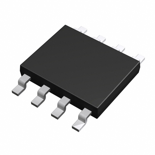
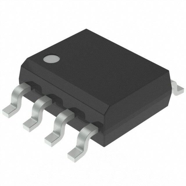
- 型号: MR44V064AMAZAAB
- 制造商: ROHM Semiconductor
- 库位|库存: xxxx|xxxx
- 要求:
| 数量阶梯 | 香港交货 | 国内含税 |
| +xxxx | $xxxx | ¥xxxx |
查看当月历史价格
查看今年历史价格
MR44V064AMAZAAB产品简介:
ICGOO电子元器件商城为您提供MR44V064AMAZAAB由ROHM Semiconductor设计生产,在icgoo商城现货销售,并且可以通过原厂、代理商等渠道进行代购。 MR44V064AMAZAAB价格参考。ROHM SemiconductorMR44V064AMAZAAB封装/规格:存储器, FRAM (Ferroelectric RAM) Memory IC 64Kb (8K x 8) I²C 3.4MHz 130ns 8-SOP。您可以下载MR44V064AMAZAAB参考资料、Datasheet数据手册功能说明书,资料中有MR44V064AMAZAAB 详细功能的应用电路图电压和使用方法及教程。
| 参数 | 数值 |
| 产品目录 | 集成电路 (IC) |
| 描述 | IC FRAM 64KBIT 3.4MHZ 8SOP |
| 产品分类 | |
| 品牌 | Rohm Semiconductor |
| 数据手册 | |
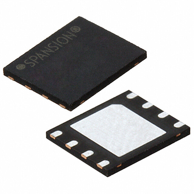
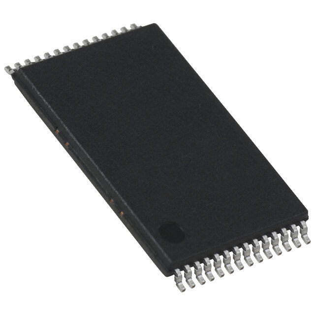
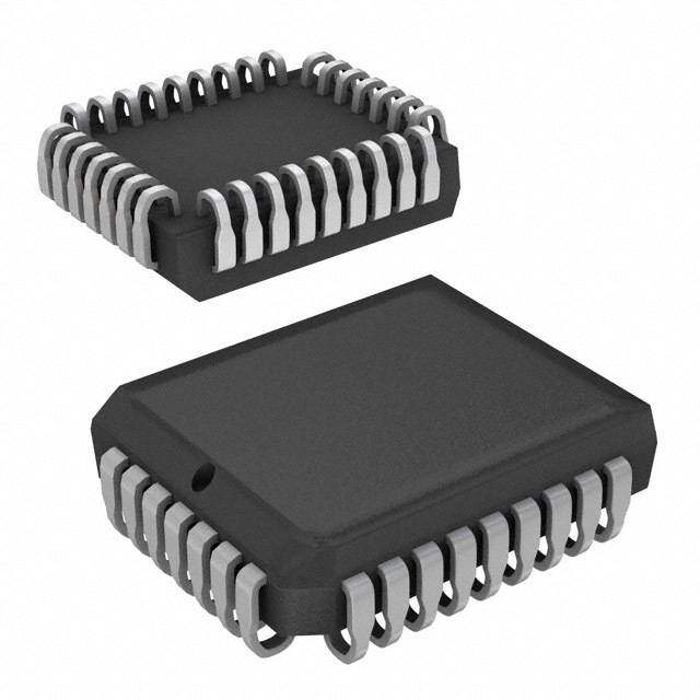
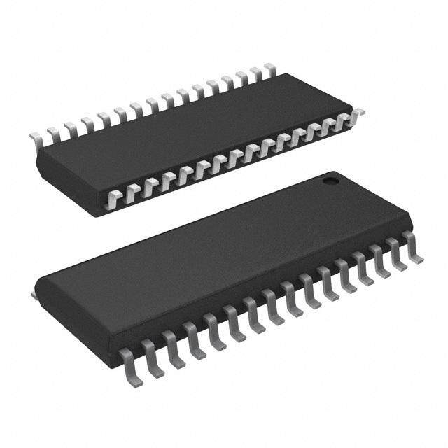
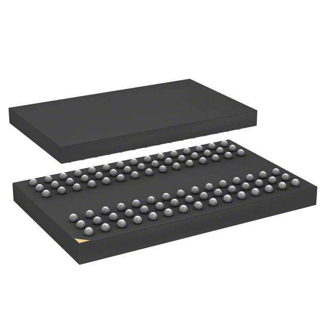
| 产品图片 |
|
| 产品型号 | MR44V064AMAZAAB |
| rohs | 无铅 / 符合限制有害物质指令(RoHS)规范要求 |
| 产品系列 | - |
| 供应商器件封装 | 8-SOP |
| 其它名称 | MR44V064AMAZAABDKR |
| 包装 | Digi-Reel® |
| 存储器类型 | FRAM(Ferroelectric RAM) |
| 存储容量 | 64K (8K x 8) |
| 封装/外壳 | 8-SOIC(0.154",3.90mm 宽) |
| 工作温度 | -40°C ~ 85°C |
| 接口 | I²C,2 线串口 |
| 标准包装 | 1 |
| 格式-存储器 | RAM |
| 电压-电源 | 2.5 V ~ 3.6 V |
| 速度 | 3.4MHz |





- 商务部:美国ITC正式对集成电路等产品启动337调查
- 曝三星4nm工艺存在良率问题 高通将骁龙8 Gen1或转产台积电
- 太阳诱电将投资9.5亿元在常州建新厂生产MLCC 预计2023年完工
- 英特尔发布欧洲新工厂建设计划 深化IDM 2.0 战略
- 台积电先进制程称霸业界 有大客户加持明年业绩稳了
- 达到5530亿美元!SIA预计今年全球半导体销售额将创下新高
- 英特尔拟将自动驾驶子公司Mobileye上市 估值或超500亿美元
- 三星加码芯片和SET,合并消费电子和移动部门,撤换高东真等 CEO
- 三星电子宣布重大人事变动 还合并消费电子和移动部门
- 海关总署:前11个月进口集成电路产品价值2.52万亿元 增长14.8%

PDF Datasheet 数据手册内容提取
FEDR44V064A-02 Issue Date: Sep. 1, 2017 MR44V064A 64k Bit(8,192-Word × 8-Bit) FeRAM (Ferroelectric Random Access Memory) I2C GENERAL DESCRIPTION The MR44V064A is a nonvolatile 8,192-word x 8-bit ferroelectric random access memory (FeRAM) developed in the ferroelectric process and silicon-gate CMOS technology. The MR44V064A is accessed using Two-wire Serial Interface ( I2C BUS ).Unlike SRAMs, this device, whose cells are nonvolatile, eliminates battery backup required to hold data. This device has no mechanisms of erasing and programming memory cells and blocks, such as those used for various EEPROMs. Therefore, the write cycle time can be equal to the read cycle time and the power consumption during a write can be reduced significantly. The MR44V064A can be used in various applications, because the device is guaranteed for the write/read tolerance of 1012 cycles per bit and the rewrite count can be extended significantly. FEATURES • 8,192-word × 8-bit configuration I2C BUS Interface • A single 3.3 V typ (2.5V to 3.6V) power supply • Operating frequency: 3.4MHz(Max) HS-mode 400KHz(Max) F/S-mode • Read/write tolerance 1012 cycles/bit • Data retention 10 years • Guaranteed operating temperature range −40 to 85°C • Package options: 8-pin plastic SOP (P-SOP8-200-1.27-T2K) • RoHS (Restriction of hazardous substances) compliant 1/16
FEDR44V064A-02 MR44V064A PIN CONFIGURATION 8-pin plastic SOP A0 1 8 VCC M R A1 2 4 7 WP 4V A2 3 06 6 SCL 4A VSS 4 5 SDA PIN DESCRIPTIONS Pin Name Description Address ( input ) A0 – A2 Address pin indicates device address. When Address value is match the device address code from SDA, the device will be selected. The address pins are pulled down internally. Serial data input serial data output ( input / output ) SDA SDA is a bi-directional line for I2C interface. The output driver is open-drain. A pull-up resistor is required. Serial Clock ( input ) SCL Serial Clock is the clock input pin for setting for serial data timing. Inputs are latched on the rising edge and outputs occur on the falling edge. Write protect ( input ) Write Protect pin controls write-operation to the memory. When WP is high, all address in WP the memory will be protected. When WP is low, all address in the memory will be written. WP pin is pulled down internally. Power supply V , V CC SS Apply the specified voltage to V . Connect V to ground. CC SS 2/16
FEDR44V064A-02 MR44V064A I2C BUS The MR44V064A employs a bi-directional two-wire I2C BUS interface, works as a slave device. An example of I2C interface system with MR44V064A Pull-up resistor SCL SDA SCL SDA SCL SDA SCL SDA I2C BUS MR44V064A MR44V064A master (slave) (slave) A2 A1 A0 A2 A1 A0 0 0 0 0 0 1 I2C BUS COMUNICATION I2C BUS data communication starts by start condition input, and ends by stop condition input. Data is always 8bit long, acknowledge is always required after each byte. I2C BUS carries out data transmission with plural devices connected by 2 communication lines of serial data ( SDA ) and serial clock ( SCL ). 1-7 8 9 1-7 8 9 1-7 8 9 SCL SDA START ADDRESS R/W ACK DATA ACK DATA ACK STOP condition condition START CONDITION Before executing each command, start condition ( start bit ) where SDA goes from “HIGH” down to “LOW” when SCL is “HIGH” is necessary. MR44V064A always detects whether SDA and SCL are in start condition ( start bit ) or not, therefore, unless this condition is satisfied, any command is executed. STOP CONDITION Each command can be ended by SDA rising from “LOW” to “HIGH” when stop condition ( stop bit ), namely,SCL is “HIGH”. 3/16
FEDR44V064A-02 MR44V064A ACKNOWLEDGE ( ACK ) SIGNAL This acknowledge ( ACK ) signal is a software rule to show whether data transfer has been made normally or not. In master and slave, the device (μ-COM at slave address input of write command, read command, and this IC at data output of read command) at the transmitter (sending) side releases the bus after output of 8bit data. The device (this IC at slave address input of write command, read command, and μ-COM at data output of read command) at the receiver (receiving) side sets SDA “LOW” during 9 clock cycles, and outputs acknowledge signal ( ACK signal) showing that it has received the 8bit data. This IC, after recognizing start condition and slave address (8bit), outputs acknowledge signal ( ACK signal) “LOW”. Each write action outputs acknowledge signal ( ACK signal ) “LOW”, at receiving 8bit data ( word address and write data ). Each read action outputs 8bit data ( read data ), and detects acknowledge signal ( ACK signal ) “LOW”. When acknowledge signal ( ACK signal ) is detect, and stop condition is not sent from the master (μ-COM) side, this IC continues data output. When acknowledge signal ( ACK signal ) is not detected, this IC stops data transfer, and recognizes stop condition ( stop bit ), and ends read action. And this IC gets in status. SLAVE ADDRESS Output slave address after start condition from master. The significant 4 bits of slave address are used for recognizing a device type. The device code of this IC is fixed to “1010”. Next slave addresses (A2 A1 A0 … device address) are for selecting devices, and plural ones can be used on a same bus according to the number of device addresses. The most insignificant bit (R/W…READ/WRITE) of slave address is used for designating write or read action, and is as shown below. Setting R/W to 0 write (setting 0 to word address setting of random read) Setting R/W to 1 read 1 2 3 4 5 6 7 8 9 1 2 SCL SDA 1 0 1 0 A2 A1 A0 R/W START ACK condition WRITE PROTECT When WP terminal is set Vcc(H level), data rewrite of all addresses is prohibited. When it is set Vss(L level), data rewrite of all address is enabled. Be sure to connect this terminal to Vcc or Vss, or control it to H level or L level. Because this terminal is pulled down internally, in the case of Open the terminal will be recognized as L level During write cycle WP terminal must be always “L” level. WP terminal must be fixed from start condition to stop condition. 4/16
FEDR44V064A-02 MR44V064A WRITE COMMAND BYTE WRITE CYCLE Arbitrary data is written to FeRAM. When to write only 1 byte, byte write is normally used. start condition slave address with LSB is 0 (write) 1st and 2nd word address byte of write data. stop condition S W S T R T A I O R Slave address T 1st WORD address 2nd WORD address Write data P T E W W W W 1 0 1 0 A2 A1 A0 0 0 0 A A A A D D 12 8 7 0 7 0 A A A A C C C C K K K K PAGE WRITE CYCLE When to write continuous data of 2 bytes or more, simultaneous write is possible by page write cycle. The address reaches the final address, the address will be rolled over to the first address. By page write cycle, up to 8,192 bytes data can be written. When data above the maximum bytes are sent, data from the first byte will be overwritten. S W S T R T A I O R Slave address T 1st WORD address 2nd WORD address Write data Write data P T E 1 0 1 0 A2 A1 A0 0 0 0 WA WA WA WA D D D D 12 8 7 0 7 0 7 0 A A A A A C C C C C K K K K K READ COMMAND CURRENT READ CYCLE Current read cycle is a command to read data of internal address register without designating address. When the last read address is (n)-th address just before current read cycle, the current read command outputs data of (n+1)-th address. When the last write address is (n)-th address just before current read cycle, the current read command outputs data of (n)-th address. The previous read or write sequence should be complete up to stop condition. Just after POWER ON, the internal address resister is unstable. S R S T E T A A O R Slave address D Read data P T 1 0 1 0 A2 A1 A0 D7 D0 A N C A K C K 5/16
FEDR44V064A-02 MR44V064A RANDOM READ CYCLE Random read cycle is a command to read data by designating address. start condition slave address with LSB is 0 (write) 1st and 2nd word address start condition slave address with LSB is 1 (read) read out byte of data. ACK to “H” stop condition S W S R S T R T E T A I A A O R Slave address T 1st WORD address 2nd WORD address R Slave address D Read data P T E T W W W W 1 0 1 0 A2 A1 A0 0 0 0 A A A A 1 0 1 0A2A1A0 D D 12 8 7 0 7 0 A A A A N C C C C A K K K K C K SEQUENTIAL READ CYCLE When ACK signal “L” after D0 is detected, and stop condition is not sent from master side, the next address data can be read in succession. The address reaches the final address, the address will be rolled over to the first address. S W S R S T R T E T A I A A O R Slave address T 1st WORD address 2nd WORD address R Slave address D Read data P T E T W W W W 1 0 1 0 A2 A1 A0 0 0 0 A A A A 1 0 1 0A2A1A0 D D D 12 8 7 0 0 7 0 A A A A A N C C C C C DA K K K K K C7 K HIGH SPEED MODE The MR44V064A support a maximum 3.4MHz high speed mode. When HS-mode operation is needed, the HS-mode command is required before any command. After the HS-mode command is issued, MR44V064A will be the HS-mode, until stop condition is issued. CURRENT ADDRESS READ CYCLE ( HS-MODE ) S S R S T T E T A A A O R HS-mode command R Slave address D Read data P T T 0 0 0 0 1 X X X 1 0 1 0 A2 A1 A0 D7 D0 NA CA NA C K C K K BYTE WRITE CYCLE ( HS-MODE ) S S W S T T R T A A I O R HS-mode command R Slave address T 1stWORD address 2ndWORD address Write data P T T E W W W W 0 0 0 0 1 X X X 1 0 1 0 A2 A1 A0 0 0 0 A A A A D D 12 8 7 0 7 0 N A A A A A C C C C C K K K K K 6/16
FEDR44V064A-02 MR44V064A ELECTRICAL CHARACTERISTICS ABSOLUTE MAXIMUM RATINGS The application of stress (voltage, current, or temperature) that exceeds the absolute maximum rating may damage the device. Therefore, do not allow actual characteristics to exceed any one parameter ratings PIN VOLTAGES Rating Parameter Symbol Unit Note Min. Max. Pin Voltage (Input Signal) VIN –0.5 VCC + 0.5 V Pin Voltage (Input/Output VINQ, VOUTQ –0.5 VCC + 0.5 V Voltage) Power Supply Voltage VCC –0.5 4.0 V TEMPERATURE RANGE Rating Parameter Symbol Unit Note Min. Max. Storage Temperature Tstg –55 125 °C Operating Temperature Topr –40 85 °C OTHERS Ta=25°C Parameter Symbol Rating Note Power Dissipation PD 1,000mW Allowable Input Current IIN +/- 20mA Ta=25°C Allowable Output Current IOUT +/- 20mA Ta=25°C 7/16
FEDR44V064A-02 MR44V064A RECOMMENDED OPERATING CONDITIONS POWER SUPPLY VOLTAGE Parameter Symbol Min. Typ. Max. Unit Note Power Supply Voltage VCC 2.5 3.3 3.6 V Ground Voltage VSS 0 0 0 V DC INPUT VOLTAGE Parameter Symbol Min. Max. Unit Note Input High Voltage VIH VCC x 0.7 VCC+0.3 V Input Low Voltage VIL –0.3 VCC x 0.3 V 8/16
FEDR44V064A-02 MR44V064A DC CHARACTERISTICS DC INPUT/OUTPUT CHARACTERISTICS Parameter Symbol Condition Min. Max. Unit Note Output Low Voltage VOL IOL =2mA ― 0.4 V Input Leakage Current ILI ― –10 10 µA Output Leakage ILO ― –10 10 µA Current POWER SUPPLY CURRENT V =Max.to Min, Ta=Topr CC Parameter Symbol Condition Max. Unit Note Power Supply SCL,SDA= VCC, Current ICCS 400 µA (Standby) A2,A1,A0,WP= VCC or VSS Power Supply fSCL=3.4MHz 1 mA Current ICCA fSCL=400KHz 600 uA (Operating) 9/16
FEDR44V064A-02 MR44V064A AC CHARACTERISTICS V =Max. to Min., Ta=Topr. CC F/S-mode HS-mode Parameter Symbol Unit Note Min. Max. Min. Max. Clock frequency fSCL D.C. 400 DC 3400 KHz Clock Low time tLOW 1300 160 ns Clock High time tHIGH 600 60 ns Output Data delay time tAA 900 130 ns BUS release time before tBUF 1300 300 ns transfer start Start condition hold time tHD:STA 600 160 ns Start condition setup time tSU:STA 600 160 ns Input data hold time tHD:DAT 0 0 ns Input data setup time tSU:DAT 100 10 ns SDA, SCL rise time tR 300 80 ns 1 SDA, SCL fall time tF 300 80 ns 1 Stop condition setup time tSU:STO 600 160 ns Output data hold time tDH 0 0 ns Noise removal time (SDA, tSP 50 5 ns SCL) Note: 1. Not 100% tested Equivalent AC Load Circuit 3.3V 1kΩ Output 100pF 10/16
FEDR44V064A-02 MR44V064A TIMING 1/fSCL tR tF tHIGH tSP tSP SCL VIH VIH VIH VIH VIH VIH VIL VIL VIL VIL VIL VIL tF tSU:DAT tLOW tHD:DAT SDA VIH VIH VIH (input) VIL VIL VIL tR tBUF tAA tDH SDA VIH VIH (output) VIL VIL SCL VIH VIH VIH tSU:STA tHD:STA tSU:STO SDA VIH (input) VIL VIL START BIT STOP BIT 11/16
FEDR44V064A-02 MR44V064A •POWER-ON AND POWER-OFF CHARACTERISTICS (Under recommended operating conditions) Parameter Symbol Min. Max. Unit Note Power-On SCL,SDA High Hold Time t 50 ⎯ μs 1, 2 VHEL Power-Off SCL, SDA High Hold Time t 100 ⎯ ns 1 EHVL Power-On Interval Time t 1 ⎯ μs 2 VLVH Notes: 1. To prevent an erroneous operation, be sure to maintain SCL=SDA="H", and set the FeRAM in an inactive state (standby mode) before and after power-on and power-off. 2. Powering on at the intermediate voltage level will cause an erroneous operation; thus, be sure to power up from 0 V. 3. Enter all signals at the same time as power-on or enter all signals after power-on. •Power-On and Power-Off Sequences t t EHVL VHEL VCC VCC VCC Min. VCC Min. VIH Min. VIH Min. t VLVH VIL Max. VIL Max. S CL,SDA SCL,SDA 0V 0V • After Power-Off, terminal state When MR44V064A only goes power-off while the other IC’s on I2C bus are active, all the input pins including I/O pin of MR44V064A must be GND level. 12/16
FEDR44V064A-02 MR44V064A READ/WRITE CYCLES AND DATA RETENTION (Under recommended operating conditions) Parameter Min. Max. Unit Note Read/Write Cycle 1012 ⎯ Cycle Data Retention 10 ⎯ Year CAPACITANCE V =3.3V, V = V = GND, f = 1MHz, and Ta = 25°C CC IN OUT Signal Symbol Min. Max. Unit Note Input Capacitance CIN ⎯ 10 pF 1 Input/Output Capacitance COUT ⎯ 10 pF 1 Note: 1. Sampling value. 13/16
FEDR44V064A-02 MR44V064A PACKAGE DIMENSIONS (Unit: mm) Notes for Mounting the Surface Mount Type Package The surface mount type packages are very susceptible to heat in reflow mounting and humidity absorbed in storage. Therefore, before you perform reflow mounting, contact a ROHM sales office for the product name, package name, pin number, package code and desired mounting conditions (reflow method, temperature and times). 14/16
FEDR44V064A-02 MR44V064A REVISION HISTORY Page Document No. Date Previous Current Description Edition Edition FEDR44V064A-01 Apr. 22, 2013 – – Final edition 1 1 1 Changed New company logo. 9 9 Corrected a condition of power supply current 11 11 Added VIH/VIL FEDR44V064A-02 Sep. 01, 2017 12 12 Added “After Power-Off, terminal state” 16 16 Changed Notes – – Corrected a vague description. 15/16
FEDR44V064A-02 MR44V064A Notes 1) The information contained herein is subject to change without notice. 2) Although LAPIS Semiconductor is continuously working to improve product reliability and quality, semiconductors can break down and malfunction due to various factors. Therefore, in order to prevent personal injury or fire arising from failure, please take safety measures such as complying with the derating characteristics, implementing redundant and fire prevention designs, and utilizing backups and fail-safe procedures. LAPIS Semiconductor shall have no responsibility for any damages arising out of the use of our Products beyond the rating specified by LAPIS Semiconductor. 3) Examples of application circuits, circuit constants and any other information contained herein are provided only to illustrate the standard usage and operations of the Products. The peripheral conditions must be taken into account when designing circuits for mass production. 4) The technical information specified herein is intended only to show the typical functions of the Products and examples of application circuits for the Products. No license, expressly or implied, is granted hereby under any intellectual property rights or other rights of LAPIS Semiconductor or any third party with respect to the information contained in this document; therefore LAPIS Semiconductor shall have no responsibility whatsoever for any dispute, concerning such rights owned by third parties, arising out of the use of such technical information. 5) The Products are intended for use in general electronic equipment (i.e. AV/OA devices, communication, consumer systems, gaming/entertainment sets) as well as the applications indicated in this document. 6) The Products specified in this document are not designed to be radiation tolerant. 7) For use of our Products in applications requiring a high degree of reliability (as exemplified below), please contact and consult with a LAPIS Semiconductor representative: transportation equipment (i.e. cars, ships, trains), primary communication equipment, traffic lights, fire/crime prevention, safety equipment, medical systems, servers, solar cells, and power transmission systems. 8) Do not use our Products in applications requiring extremely high reliability, such as aerospace equipment, nuclear power control systems, and submarine repeaters. 9) LAPIS Semiconductor shall have no responsibility for any damages or injury arising from non-compliance with the recommended usage conditions and specifications contained herein. 10) LAPIS Semiconductor has used reasonable care to ensure the accuracy of the information contained in this document. However, LAPIS Semiconductor does not warrant that such information is error-free and LAPIS Semiconductor shall have no responsibility for any damages arising from any inaccuracy or misprint of such information. 11) Please use the Products in accordance with any applicable environmental laws and regulations, such as the RoHS Directive. For more details, including RoHS compatibility, please contact a ROHM sales office. LAPIS Semiconductor shall have no responsibility for any damages or losses resulting non-compliance with any applicable laws or regulations. 12) When providing our Products and technologies contained in this document to other countries, you must abide by the procedures and provisions stipulated in all applicable export laws and regulations, including without limitation the US Export Administration Regulations and the Foreign Exchange and Foreign Trade Act. 13) This document, in part or in whole, may not be reprinted or reproduced without prior consent of LAPIS Semiconductor. Copyright 2013 – 2017 LAPIS Semiconductor Co., Ltd. 2-4-8 Shinyokohama, Kouhoku-ku, Yokohama 222-8575, Japan http://www.lapis-semi.com/en/ 16/16
 Datasheet下载