
 Datasheet下载
- 型号: MR25H10CDF
- 制造商: EVERSPIN TECHNOLOGIES
- 库位|库存: xxxx|xxxx
- 要求:
| 数量阶梯 | 香港交货 | 国内含税 |
| +xxxx | $xxxx | ¥xxxx |
查看当月历史价格
查看今年历史价格
MR25H10CDF产品简介:
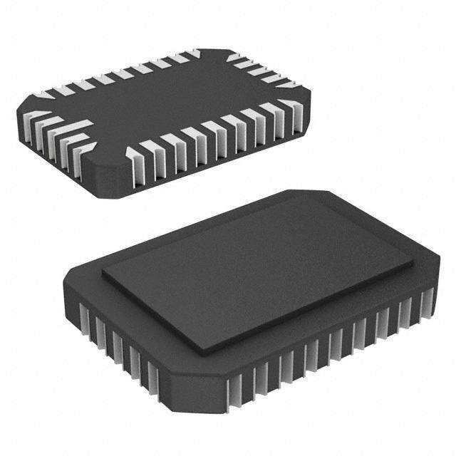
ICGOO电子元器件商城为您提供MR25H10CDF由EVERSPIN TECHNOLOGIES设计生产,在icgoo商城现货销售,并且可以通过原厂、代理商等渠道进行代购。 MR25H10CDF价格参考。EVERSPIN TECHNOLOGIESMR25H10CDF封装/规格:存储器, MRAM(磁阻式 RAM) 存储器 IC 1Mb (128K x 8) SPI 40MHz 8-DFN-EP,小标志(5x6)。您可以下载MR25H10CDF参考资料、Datasheet数据手册功能说明书,资料中有MR25H10CDF 详细功能的应用电路图电压和使用方法及教程。
Everspin Technologies Inc.生产的MR25H10CDF是一款基于磁阻随机存取存储器(MRAM)技术的存储器。这款存储器具有非易失性、高速读写和低功耗的特点,适用于多种应用场景。

1. 工业自动化:
在工业自动化领域,MR25H10CDF可用于保存关键配置数据、校准参数和运行日志。由于其非易失性和高可靠性,即使在断电情况下也能确保数据的安全性和完整性,特别适合用于工厂自动化控制系统、机器人控制器和传感器网络中。

2. 汽车电子:
汽车电子系统对存储器的可靠性和耐久性要求极高。MR25H10CDF可用于汽车发动机控制单元(ECU)、防抱死制动系统(ABS)、电子稳定程序(ESP)等关键子系统的数据存储。其快速响应和高耐久性有助于提高车辆的安全性和性能。

3. 通信设备:
在通信基础设施中,如基站、路由器和交换机,MR25H10CDF可以用来存储配置文件、固件更新和日志信息。其高速读写性能和低功耗特性使其成为通信设备的理想选择,特别是在需要频繁读写操作的场景下。

4. 物联网(IoT)设备:
物联网设备通常需要在有限的电源条件下长时间运行,并且需要频繁地保存和读取数据。MR25H10CDF的低功耗和非易失性特点非常适合应用于智能家居、智能城市和工业物联网设备中,确保数据的可靠性和实时性。

5. 数据中心与服务器:
数据中心和服务器需要高性能和高可靠的存储解决方案。MR25H10CDF可以在缓存、日志记录和临时数据存储方面发挥作用,提供快速的数据访问速度和持久的数据保护,减少因断电或故障导致的数据丢失风险。

总之,MR25H10CDF凭借其独特的技术优势,广泛应用于各种需要高可靠性、高速度和低功耗的场景中,为不同行业的用户提供卓越的存储解决方案。
| 参数 | 数值 |
| 产品目录 | 集成电路 (IC)半导体 |
| 描述 | IC MRAM 1MBIT 40MHZ 8DFNNVRAM 1Mb 3.3V 128Kx8 Serial MRAM |
| 产品分类 | |
| 品牌 | Everspin Technologies |
| 产品手册 | |
| 产品图片 |
|
| rohs | 符合RoHS无铅 / 符合限制有害物质指令(RoHS)规范要求 |
| 产品系列 | 内存,NVRAM,Everspin Technologies MR25H10CDF- |
| 数据手册 | |
| 产品型号 | MR25H10CDF |
| 产品种类 | NVRAM |
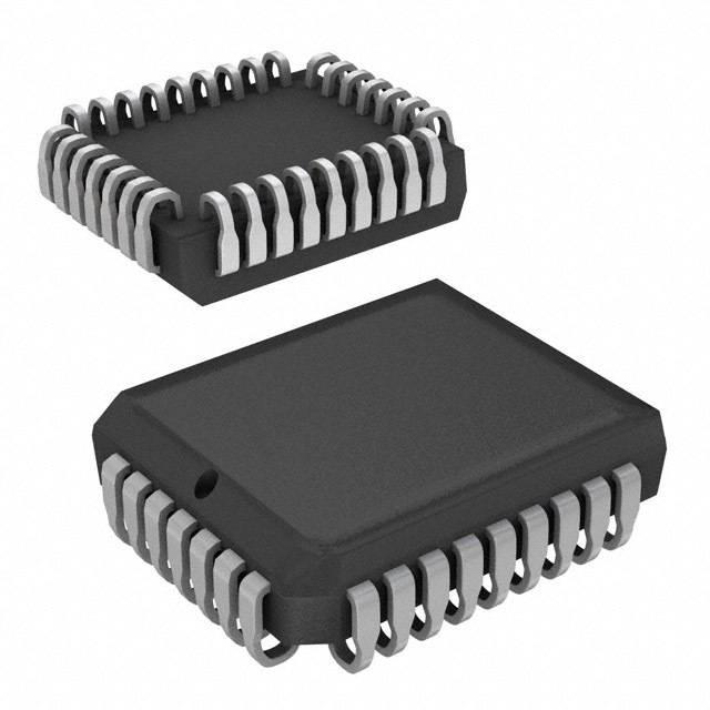
| 供应商器件封装 | 8-DFN-EP,小标志 (5x6) |
| 其它名称 | 819-1039 |
| 包装 | 托盘 |
| 商标 | Everspin Technologies |
| 存储器类型 | MRAM(磁阻 RAM) |
| 存储容量 | 1 Mbit |
| 封装 | Tray |
| 封装/外壳 | 8-VDFN 裸露焊盘 |
| 封装/箱体 | DFN-8 |
| 工作温度 | -40°C ~ 85°C |
| 工作温度范围 | - 40 C to + 85 C |
| 工作电压 | 2.7 V to 3.6 V |
| 工作电流 | 20 mA |
| 工厂包装数量 | 570 |
| 接口 | SPI 串行 |
| 接口类型 | SPI |
| 数据总线宽度 | 8 bit |
| 最大功率耗散 | 0.6 W |
| 最大工作温度 | + 85 C |
| 最小工作温度 | - 40 C |
| 标准包装 | 570 |
| 格式-存储器 | RAM |
| 电压-电源 | 2.7 V ~ 3.6 V |
| 电源电压-最大 | 3.6 V |
| 电源电压-最小 | 2.7 V |
| 系列 | MR25H10 |
| 组织 | 128 k x 8 |
| 速度 | 40MHz |


- 商务部:美国ITC正式对集成电路等产品启动337调查
- 曝三星4nm工艺存在良率问题 高通将骁龙8 Gen1或转产台积电
- 太阳诱电将投资9.5亿元在常州建新厂生产MLCC 预计2023年完工
- 英特尔发布欧洲新工厂建设计划 深化IDM 2.0 战略
- 台积电先进制程称霸业界 有大客户加持明年业绩稳了
- 达到5530亿美元!SIA预计今年全球半导体销售额将创下新高
- 英特尔拟将自动驾驶子公司Mobileye上市 估值或超500亿美元
- 三星加码芯片和SET,合并消费电子和移动部门,撤换高东真等 CEO
- 三星电子宣布重大人事变动 还合并消费电子和移动部门
- 海关总署:前11个月进口集成电路产品价值2.52万亿元 增长14.8%
_renders/IS61WV102416BLL-10TLI.jpg)


_renders/IS42S32800J-6TLI.jpg)
PDF Datasheet 数据手册内容提取
MR25H10 FEATURES 1Mb Serial SPI MRAM • No write delays • Unlimited write endurance • Data retention greater than 20 years • Automatic data protection on power loss • Block write protection • Fast, simple SPI interface with up to 40 MHz clock rate • 2.7 to 3.6 Volt power supply range DFN • Low current sleep mode • Industrial temperatures • Available in 8-pin DFN or 8-pin DFN Small Flag RoHS-compliant packages • Direct replacement for serial EEPROM, Flash, FeRAM • AEC-Q100 Grade 1 Option Small Flag DFN INTRODUCTION The MR25H10 is a 1,048,576-bit magnetoresistive random access memory RoHS (MRAM) device organized as 131,072 words of 8 bits. The MR25H10 offers serial EEPROM and serial Flash compatible read/write timing with no write delays and unlimited read/write endurance. Unlike other serial memories, both reads and writes can occur randomly in memory with no delay between writes. The MR25H10 is the ideal memory solution for applications that must store and retrieve data and programs quickly using a small number of I/O pins. The MR25H10 is available in either a 5 mm x 6 mm 8-pin DFN package or a 5 mm x 6 mm 8-pin DFN Small Flag package. Both are compatible with serial EEPROM, Flash, and FeRAM products. The MR25H10 provides highly reliable data storage over a wide range of temperatures. The product is offered with Industrial (-40° to +85 °C) and AEC-Q100 Grade 1 (-40°C to +125 °C) operating temperature range options. CONTENTS 1. DEVICE PIN ASSIGNMENT......................................................................... 2 2. SPI COMMUNICATIONS PROTOCOL...................................................... 4 3. ELECTRICAL SPECIFICATIONS................................................................. 10 4. TIMING SPECIFICATIONS.......................................................................... 12 5. ORDERING INFORMATION....................................................................... 12 6. MECHANICAL DRAWING.......................................................................... 13 7. REVISION HISTORY...................................................................................... 15 How to Reach Us.......................................................................................... 15 Copyright © Everspin Technologies 2018 1 MR25H10 Rev. 9.5 3/2018
MR25H10 1. DEVICE PIN ASSIGNMENT Overview The MR25H10 is a serial MRAM with memory array logically organized as 128Kx8 using the four pin in- terface of chip select (CS), serial input (SI), serial output (SO) and serial clock (SCK) of the serial peripheral interface (SPI) bus. Serial MRAM implements a subset of commands common to today’s SPI EEPROM and Flash components allowing MRAM to replace these components in the same socket and interoperate on a shared SPI bus. Serial MRAM offers superior write speed, unlimited endurance, low standby & operating power, and more reliable data retention compared to available serial memory alternatives. Figure 1.1 Block Diagram WP Instruction Decode CS Clock Generator HOLD Control Logic SCK Write Protect 128KB MRAM ARRAY Instruction Register Address Register 17 8 Counter SO SI Data I/O Register 4 Nonvolatile Status Register System Configuration Single or multiple devices can be connected to the bus as shown in Figure 1.2. Pins SCK, SO and SI are common among devices. Each device requires CS and HOLD pins to be driven separately. Figure 1.2 System Configuration SCK MOSI MISO SO SI SCK SO SI SCK SPI EVERSPIN SPI MRAM 1 EVERSPIN SPI MRAM 2 Micro Controller CS HOLD CS HOLD CS1 HOLD1 CS2 HOLD2 MOSI = Master Out Slave In MISO = Master In Slave Out Copyright © Everspin Technologies 2018 2 MR25H10 Rev. 9.5 3/2018
MR25H10 DEVICE PIN ASSIGNMENT Figure 1.3 Pin Diagrams (Top View) CS 1 8 VDD SO 2 7 HOLD WP 3 6 SCK VS S 4 5 SI 8-Pin DFN or 8-Pin DFN Small Flag Package Table 1.1 Pin Functions Signal Name Pin I/O Function Description An active low chip select for the serial MRAM. When chip select is high, the memory is powered down to minimize standby power, inputs are ignored CS 1 Input Chip Select and the serial output pin is Hi-Z. Multiple serial memories can share a com- mon set of data pins by using a unique chip select for each memory. The data output pin is driven during a read operation and remains Hi-Z at SO 2 Output Serial Output all other times. SO is Hi-Z when HOLD is low. Data transitions on the data output occur on the falling edge of SCK. A low on the write protect input prevents write operations to the Status WP 3 Input Hold Register. V 4 Supply Ground Power supply ground pin. SS All data is input to the device through this pin. This pin is sampled on the SI 5 Input Serial Input rising edge of SCK and ignored at other times. SI can be tied to SO to create a single bidirectional data bus if desired. Synchronizes the operation of the MRAM. The clock can operate up to 40 MHz to shift commands, address, and data into the memory. Inputs are captured on the rising edge of clock. Data outputs from the MRAM occur SCK 6 Input Serial Clock on the falling edge of clock. The serial MRAM supports both SPI Mode 0 (CPOL=0, CPHA=0) and Mode 3 (CPOL=1, CPHA=1). In Mode 0, the clock is normally low. In Mode 3, the clock is normally high. Memory operation is static so the clock can be stopped at any time. A low on the Hold pin interrupts a memory operation for another task. When HOLD is low, the current operation is suspended. The device will HOLD 7 Input Hold ignore transitions on the CS and SCK when HOLD is low. All transitions of HOLD must occur while CS is low. V 8 Supply Power Supply Power supply voltage from +2.7 to +3.6 volts. DD Copyright © Everspin Technologies 2018 3 MR25H10 Rev. 9.5 3/2018
MR25H10 2. SPI COMMUNICATIONS PROTOCOL MR25H10 can be operated in either SPI Mode 0 (CPOL=0, CPHA =0) or SPI Mode 3 (CPOL=1, CPHA=1). For both modes, inputs are captured on the rising edge of the clock and data outputs occur on the falling edge of the clock. When not conveying data, SCK remains low for Mode 0; while in Mode 3, SCK is high. The memory determines the mode of operation (Mode 0 or Mode 3) based upon the state of the SCK when CS falls. All memory transactions start when CS is brought low to the memory. The first byte is a command code. De- pending upon the command, subsequent bytes of address are input. Data is either input or output. There is only one command performed per CS active period. CS must go inactive before another command can be accepted. To ensure proper part operation according to specifications, it is necessary to terminate each access by raising CS at the end of a byte (a multiple of 8 clock cycles from CS dropping) to avoid partial or aborted accesses. Table 2.1 Command Codes Instruction Description Binary Code Hex Code Address Bytes Data Bytes WREN Write Enable 0000 0110 06h 0 0 WRDI Write Disable 0000 0100 04h 0 0 RDSR Read Status Register 0000 0101 05h 0 1 WRSR Write Status Register 0000 0001 01h 0 1 READ Read Data Bytes 0000 0011 03h 3 1 to ∞ WRITE Write Data Bytes 0000 0010 02h 3 1 to ∞ SLEEP Enter Sleep Mode 1011 1001 B9h 0 0 WAKE Exit Sleep Mode 1010 1011 ABh 0 0 Status Register and Block Write Protection The status register consists of the 8 bits listed in table 2.2. Status register bits BP0 and BP1 define the mem- ory block arrays that are protected as described in table 2.3. The Status Register Write Disable bit (SRWD) is used in conjunction with bit 1 (WEL) and the Write Protection pin (WP) as shown in table 2.4 to enable writes to status register bits. The fast writing speed of MR25H10 does not require write status bits. The state of bits 6,5,4, and 0 can be user modified and do not affect memory operation. All bits in the status register are pre-set from the factory to the “0” state. Table 2.2 Status Register Bit Assignments Bit 7 Bit 6 Bit 5 Bit 4 Bit 3 Bit 2 Bit 1 Bit 0 SRWD Don’t Care Don’t Care Don’t Care BP1 BP0 WEL Don’t Care Copyright © Everspin Technologies 2018 4 MR25H10 Rev. 9.5 3/2018
MR25H10 SPI COMMUNICATIONS PROTOCOL Table 2.3 Block Memory Write Protection Status Register Memory Contents BP1 BP0 Protected Area Unprotected Area 0 0 None All Memory 0 1 Upper Quarter Lower Three-Quarters 1 0 Upper Half Lower Half 1 1 All None Table 2.4 Memory Protection Modes Status WEL SRWD WP Protected Blocks Unprotected Blocks Register 0 X X Protected Protected Protected 1 0 X Protected Writable Writable 1 1 Low Protected Writable Protected 1 1 High Protected Writable Writable When WEL is reset to 0, writes to all blocks and the status register are protected. When WEL is set to 1, BP0 and BP1 determine which memory blocks are protected. While SRWD is reset to 0 and WEL is set to 1, status register bits BP0 and BP1 can be modified. Once SRWD is set to 1, WP must be high to modify SRWD, BP0 and BP1. Read Status Register (RDSR) The Read Status Register (RDSR) command allows the Status Register to be read. The Status Register can be read at any time to check the status of write enable latch bit, status register write protect bit, and block write protect bits. For MR25H10, the write in progress bit (bit 0) is not written by the memory because there is no write delay. The RDSR command is entered by driving CS low, sending the command code, and then driving CS high. Figure 2.1 RDSR CS 0 1 2 3 4 5 6 7 0 1 2 3 4 5 6 7 Mode 3 SCK Mode 0 SI 0 0 0 0 0 1 0 1 MSB Status Register Out SO High Impedance High Z 7 6 5 4 3 2 1 0 MSB Copyright © Everspin Technologies 2018 5 MR25H10 Rev. 9.5 3/2018
MR25H10 SPI COMMUNICATIONS PROTOCOL Write Enable (WREN) The Write Enable (WREN) command sets the Write Enable Latch (WEL) bit in the status register to 1. The WEL bit must be set prior to writing in the status register or the memory. The WREN command is entered by driving CS low, sending the command code, and then driving CS high. Figure 2.2 WREN CS Mode 3 0 1 2 3 4 5 6 7 Mode 3 SCK Mode 0 Mode 0 Instruction (06h) SI 0 0 0 0 0 1 1 0 High Impedance SO Write Disable (WRDI) The Write Disable (WRDI) command resets the WEL bit in the status register to 0. This prevents writes to status register or memory. The WRDI command is entered by driving CS low, sending the command code, and then driving CS high. The WEL bit is reset to 0 on power-up or completion of WRDI. Figure 2.3 WRDI CS Mode 3 0 1 2 3 4 5 6 7 Mode 3 SCK Mode 0 Mode 0 Instruction (04h) SI 0 0 0 0 0 1 0 0 High Impedance SO Write Status Register (WRSR) The Write Status Register (WRSR) command allows new values to be written to the Status Register. The WRSR command is not executed unless the Write Enable Latch (WEL) has been set to 1 by executing a WREN command while pin WP and bit SRWD correspond to values that make the status register writable as seen in table 2.4. Status Register bits are non-volatile with the exception of the WEL which is reset to 0 upon power cycling. Copyright © Everspin Technologies 2018 6 MR25H10 Rev. 9.5 3/2018
MR25H10 SPI COMMUNICATIONS PROTOCOL The WRSR command is entered by driving CS low, sending the command code and status register write data byte, and then driving CS high.The WRSR command is entered by driving CS low, sending the com- mand code and status register write data byte, and then driving CS high. Figure 2.4 WRSR CS 0 1 2 3 4 5 6 7 8 9 10 11 12 13 14 15 Mode 3 SCK Mode 0 Instruction (01h) Status Register In SI 0 0 0 0 0 0 0 1 7 6 5 4 3 2 1 0 MSB High Impedance SO Read Data Bytes (READ) The Read Data Bytes (READ) command allows data bytes to be read starting at an address specified by the 24-bit address. Only address bits 0-16 are decoded by the memory. The data bytes are read out sequen- tially from memory until the read operation is terminated by bringing CS high The entire memory can be read in a single command. The address counter will roll over to 0000h when the address reaches the top of memory. The READ command is entered by driving CS low and sending the command code. The memory drives the read data bytes on the SO pin. Reads continue as long as the memory is clocked. The command is termi- nated by bring CS high. Figure 2.5 READ CS 0 1 2 3 4 5 6 7 8 9 10 28 29 30 31 32 33 34 35 36 37 38 39 SCK Instruction (03h) 24-Bit Address SI 0 0 0 0 0 0 1 1 X X X 3 2 1 0 MSB Data Out 1 Data Out 2 High Impedance SO 7 6 5 4 3 2 1 0 7 MSB Copyright © Everspin Technologies 2018 7 MR25H10 Rev. 9.5 3/2018
MR25H10 SPI COMMUNICATIONS PROTOCOL Write Data Bytes (WRITE) The Write Data Bytes (WRITE) command allows data bytes to be written starting at an address specified by the 24-bit address. Only address bits 0-16 are decoded by the memory. The data bytes are written sequen- tially in memory until the write operation is terminated by bringing CS high. The entire memory can be written in a single command. The address counter will roll over to 0000h when the address reaches the top of memory. Unlike EEPROM or Flash Memory, MRAM can write data bytes continuously at its maximum rated clock speed without write delays or data polling. Back to back WRITE commands to any random location in mem- ory can be executed without write delay. MRAM is a random access memory rather than a page, sector, or block organized memory so it is ideal for both program and data storage. The WRITE command is entered by driving CS low, sending the command code, and then sequential write data bytes. Writes continue as long as the memory is clocked. The command is terminated by bringing CS high. Figure 2.6 WRITE CS 0 1 2 3 4 5 6 7 8 9 10 28 29 30 31 32 33 34 35 36 37 38 39 SCK Instruction (02h) 24-Bit Address SI 0 0 0 0 0 0 1 0 X X X 3 2 1 0 7 6 5 4 3 2 1 0 MSB MSB High Impedance SO CS 40 41 42 43 44 45 46 47 48 49 50 51 52 53 54 55 Mode 3 SCK Mode 0 Data Byte 2 Data Byte 3 Data Byte N SI 7 6 5 4 3 2 1 0 7 6 5 4 3 2 1 0 7 6 5 4 3 2 1 0 MSB MSB High Impedance SO Copyright © Everspin Technologies 2018 8 MR25H10 Rev. 9.5 3/2018
MR25H10 SPI COMMUNICATIONS PROTOCOL Enter Sleep Mode (SLEEP) The Enter Sleep Mode (SLEEP) command turns off all MRAM power regulators in order to reduce the overall chip standby power to 3 μA typical. The SLEEP command is entered by driving CS low, sending the com- mand code, and then driving CS high. The standby current is achieved after time, t . DP Figure 2.7 SLEEP CS t DP 0 1 2 3 4 5 6 7 Mode 3 SCK Mode 0 Instruction (B9h) SI 1 0 1 1 1 0 0 1 Active Current Standby Current Sleep Mode Current SO Exit Sleep Mode (WAKE) The Exit Sleep Mode (WAKE) command turns on internal MRAM power regulators to allow normal operation. The WAKE command is entered by driving CS low, sending the command code, and then driving CS high. The memory returns to standby mode after t . The CS pin must remain high until the t period is over. RDP RDP Figure 2.8 WAKE CS t RDP 0 1 2 3 4 5 6 7 Mode 3 SCK Mode 0 Instruction (ABh) SI 1 0 1 0 1 0 1 1 Sleep Mode Current Standby Current SO Copyright © Everspin Technologies 2018 9 MR25H10 Rev. 9.5 3/2018
MR25H10 3. ELECTRICAL SPECIFICATIONS Absolute Maximum Ratings This device contains circuitry to protect the inputs against damage caused by high static voltages or electric fields; however, it is advised that normal precautions be taken to avoid application of any voltage greater than maximum rated voltages to these high-impedance (Hi-Z) circuits. The device also contains protection against external magnetic fields. Precautions should be taken to avoid application of any magnetic field more intense than the field intensity specified in the maximum ratings. Table 3.1 Absolute Maximum Ratings1 Symbol Parameter Conditions Limit Unit V DD Supply voltage2 -0.5 to 4.0 V V IN Voltage on any pin2 -0.5 to V + 0.5 V DD I OUT Output current per pin ±20 mA P D Package power dissipation 3 0.600 W Industrial -45 to 95 °C T Temperature under bias BIAS AEC-Q100 Grade 1 -45 to 130 °C T stg Storage Temperature -55 to 150 °C T Lead Lead temperature 3 minutes max 260 °C H max_write Maximum magnetic field exposure Write 12,000 A/m H max_read Maximum magnetic field exposure Read or Standby 1 Permanent device damage may occur if absolute maximum ratings are exceeded. Functional operation should be restricted to recommended operating conditions. Exposure to excessive voltages or magnetic fields could affect device reliability. 2 All voltages are referenced to V . The DC value of V must not exceed actual applied V by more than SS IN DD 0.5V. The AC value of V must not exceed applied V by more than 2V for 10ns with I limited to less than IN DD IN 20mA. 3 Power dissipation capability depends on package characteristics and use environment. Copyright © Everspin Technologies 2018 10 MR25H10 Rev. 9.5 3/2018
MR25H10 ELECTRICAL SPECIFICATIONS Table 3.2 Operating Conditions Symbol Parameter Grade Min Max Unit Industrial 2.7 3.6 V V Power supply voltage DD AEC-Q100 Grade1 3.0 3.6 V V Input high voltage All 2.2 V + 0.3 V IH DD V Input low voltage All -0.5 0.8 V IL Industrial -40 85 °C T Temperature under bias A AEC-Q100 Grade1 1 -40 125 °C 1 AEC-Q100 Grade 1 temperature profile assumes 10 percent duty cycle at maximum temperature (2 years out of 20-year life.) Table 3.3 DC Characteristics Symbol Parameter Conditions Min Typical Max Unit I Input leakage current - - ±1 μA LI I Output leakage current - - ±1 μA LO I = +4 mA - - 0.4 V OL V Output low voltage OL I = +100 μA - - V + 0.2v V OL SS (I = -4 mA) 2.4 - - V OH V Output high voltage OH (I = -100 μA) V - 0.2 - - V OH DD Table 3.4 Power Supply Characteristics Symbol Parameter Conditions Typical Max Unit 1 MHz 2.5 3 mA I Active Read Current DDR 40 MHz 6 10 mA 1 MHz 8 13 mA I Active Write Current DDW 40 MHz 23 27 mA I Standby Current CS high and SPI bus inactive 90 115 μA SB I Standby Sleep Mode Current CS high and SPI bus inactive 7 30 μA zz Copyright © Everspin Technologies 2018 11 MR25H10 Rev. 9.5 3/2018
MR25H10 4. TIMING SPECIFICATIONS Table 4.1 Capacitance1 Symbol Parameter Typical Max Unit C Control input capacitance - 6 pF In C Input/Output capacitance - 8 pF I/O 1 ƒ = 1.0 MHz, dV = 3.0 V, T = 25 °C, periodically sampled rather than 100% tested. A Table 4.2 AC Measurement Conditions Parameter Value Unit Logic input timing measurement reference level 1.5 V Logic output timing measurement reference level 1.5 V Logic input pulse levels 0 or 3.0 V Input rise/fall time 2 ns Output load for low and high impedance parameters See Figure 4.1 Output load for all other timing parameters See Figure 4.2 Figure 4.1 Output Load for Impedance Parameter Measurements Z = 50 Ω D Output R = 50 Ω L V = 1.5 V L Figure 4.2 Output Load for all Other Parameter Measurements 3.3 V 590 Ω Output 435 Ω 30 pF Copyright © Everspin Technologies 2018 12 MR25H10 Rev. 9.5 3/2018
MR25H10 TIMING SPECIFICATIONS Power-Up Timing The MR25H10 is not accessible for a start-up time, t = 400 μs after power up. Users must wait this time PU from the time when V (min) is reached until the first CS low to allow internal voltage references to become DD stable. The CS signal should be pulled up to V so that the signal tracks the power supply during power-up DD sequence. Table 4.3 Power-Up Symbol Parameter Min Typical Max Unit V Write Inhibit Voltage 2.2 - 2.7 V WI t Startup Time 400 - - μs PU Figure 4.3 Power-Up Timing V DD V (max) DD Chip Selection not allowed V (min) DD Reset state t Normal Operation PU of the device V WI Time Copyright © Everspin Technologies 2018 13 MR25H10 Rev. 9.5 3/2018
MR25H10 TIMING SPECIFICATIONS Table 4.4 AC Timing Parameters1 Synchronous Data Timing Symbol Parameter Conditions Min Max Unit f SCK Clock Frequency 0 40 MHz SCK t Input Rise Time - 50 ns RI t Input Fall Time - 50 ns RF t SCK High Time 11 - ns WH t SCK Low Time 11 - ns WL Synchronous Data Timing (See figure 4.4) t CS High Time 40 - ns CS t CS Setup Time 10 - ns CSS t CS Hold Time 10 - ns CSH t Data In Setup Time 5 - ns SU t Data In Hold Time 5 - ns H V =2.7 to Output Valid Industrial Grade DD 0 10 ns 3.6v. V =3.0 to t Output Valid Industrial Grade DD 0 9 ns V 3.6v. V =3.0 to Output Valid AEC-Q100 Grade 1 DD 0 10 ns 3.6v. t Output Hold Time 0 - ns HO HOLD Timing (See figure 4.5) t HOLD Setup Time 10 - ns HD t HOLD Hold Time 10 - ns CD t HOLD to Output Low Impedance - 20 ns LZ t HOLD to Output High Impedance - 20 ns HZ Other Timing Specifications t WP Setup To CS Low 5 - ns WPS t WP Hold From CS High 5 - ns WPH t Sleep Mode Entry Time 3 - μs DP t Sleep Mode Exit Time 400 - μs RDP t Output Disable Time 12 - ns DIS 1 Over the Operating Temperature Range and C= 30 pF L Copyright © Everspin Technologies 2018 14 MR25H10 Rev. 9.5 3/2018
MR25H10 Figure 4.4 Synchronous Data Timing Figure 4.5 HOLD Timing CS t CD t CD SCK t HD t HD HOLD t t HZ LZ SO Copyright © Everspin Technologies 2018 15 MR25H10 Rev. 9.5 3/2018
MR25H10 5. ORDERING INFORMATION Figure 5.1 Part Numbering System MR 25H 10 C DC Package Options DC 8 Pin DFN on Tray DCR 8 Pin DFN on Tape and Reel DF 8 pin DFN Small Flag on Tray DFR 8 pin DFN Small Flag on Tape and Reel Temperature Range C -40 to +85 °C ambient (Industrial) M -40 to +125 °C ambient (AEC-Q100 Grade 1) Memory Density 10 1 Mb Interface 25H High Speed Serial SPI Family Product Type MR Magnetoresistive RAM Table 5.1 Available Parts Temperature Grade Package Shipping Container Order Part Number Range Tray MR25H10CDC 1 1 8-DFN Tape and Reel MR25H10CDCR 1 Industrial -40 to +85 C Tray MR25H10CDF Small Flag 8-DFN Tape and Reel MR25H10CDFR Tray MR25H10MDC 1 1 8-DFN Tape and Reel MR25H10MDCR 1 AEC-Q100 Grade 1 -40 to +125 C Tray MR25H10MDF Small Flag 8-DFN Tape and Reel MR25H10MDFR Note: 1. The DC pckage option (8-DFN) is not recommended for new designs. Please select the DF (small flag 8-DFN) option for new designs. Copyright © Everspin Technologies 2018 16 MR25H10 Rev. 9.5 3/2018
MR25H10 6. MECHANICAL DRAWINGS Figure 6.1 DFN Package Dimension A B C D E F G H I J K L M N Max. 5.10 6.10 1.00 1.27 0.45 0.05 0.35 0.70 4.20 4.20 0.261 0.05 C0.35 R0.20 Min. 4.90 5.90 0.90 BSC 0.35 0.00 Ref. 0.50 4.00 4.00 0.195 0.00 NOTE: 1. All dimensions are in mm. Angles in degrees. 2. Coplanarity applies to the exposed pad as well as the terminals. Coplanarity shall be within 0.08 mm. 3. Warpage shall not exceed 0.10 mm. 4. Refer to JEDEC MO-229 Copyright © Everspin Technologies 2018 17 MR25H10 Rev. 9.5 3/2018
MR25H10 6. MECHANICAL DRAWINGS Figure 6.2 Small Flag DFN Package Exposed metal Pad. Do not con- nect anything except V A SS 2X 0.10 C 5 8 2X 0.10 C J B I L G M H Pin 1 Index 4 1 C Detail A F K N D E Detail A Dimension A B C D E F G H I J K L M N Max 5.10 6.10 0.90 1.27 0.45 0.05 1.60 0.70 2.10 2.10 .210 0.05 C0.45 R0.20 Min 4.90 5.90 0.80 BSC 0.35 0.00 1.20 0.50 1.90 1.90 .196 0.00 NOTE: 1. All dimensions are in mm. Angles in degrees. 2. Coplanarity applies to the exposed pad as well as the terminals. Coplanarity shall be within 0.08 mm. 3. Warpage shall not exceed 0.10 mm. 4. Refer to JEDEC MO-229 Copyright © Everspin Technologies 2018 18 MR25H10 Rev. 9.5 3/2018
MR25H10 7. REVISION HISTORY Revision Date Description of Change 0 Sep 12, 2008 Initial Advance Information Release Change ac load resistance, tPU to 400 us, tRDP to 400 us, Change # of Address Bytes in Table 1 Jul 10, 2009 2 to 3, New Package Drawing, Make Preliminary 2 Jul 16, 2009 Increase Absolute Max Magnetic Field during write, read, and standby to 12,000 A/m 3 Jan 5, 2010 Described block protect in detail with power sequencing. 4 Feb 5, 2010 Added section system configuration. 5 May 17, 2010 Removed commercial specifications. All parts meet industrial specifications. Corrected various typos. Clarified block and status register protection description. Revised 6 Sep 14, 2011 Table 3.4 Power Supply specifications. Added AEC-Q100 Grade 1 ordering option. Revised Table 3.1, Table 3.2, Table 4.4 revised and Note 2 deleted, revised Figure 5.1 and Table 5.1. Corrected V in Table 3.3 to read V Max = V + 0.2v. Operating Conditions Power Supply OL OL SS Voltage for AEC-Q100 Grade1revised to 3.0-3.6v. Table 4.4: Output Valid t specifications V revised to include V ranges for Industrial and AEC-Q100 Grade 1 options. Corrected SI DD November 18, waveform in Figure 2.8. Output Valid, t for AEC-Q100 Grade revised from 9ns max to 10ns 7 v 2011 max in Table 4.4. New Small Flag DFN package option added to Page 1 Features and avail- able parts Table 5.1. DFN Small Flag drawing and dimensions table added as Figure 6.2. Figure 6.1, DFN Package, cleaned up with better quality drawing and dimension table. No specifications were changed in Figure 6.1. Reformatted tables for Section 3 Electrical Characteristics and timing parameters, Table 4.4. Revised Ordering Part Numbers Table 5.1. Removed MDF and MDFR options. MDC October 19, 8 and MDCR options are now qualified. Added Small Flag DFN illustrations. Revised 8-DFN 2012 package drawing to show correct proportion for flag and package. Corrected errors in DFN package outline drawings. Corrected V range for AEC-Q100 tV specification. DD 9 April 17, 2013 Added Automotive Grade AEC-Q100 Grade 1 for Small Flag DFN package. 9.1 May 19, 2015 Revised Everspin contact information. 9.2 June 11, 2015 Corrected Japan Sales Office telephone number. Changed all large flag DFN optoins to “The DC pckage option (8-DFN) is not recom- December 13, 9.3 mended for new designs. Please select the DF (small flag 8-DFN) option for new 2016 designs.” t t 9.4 February 2, 2017 Added HO and V relationship to Synchronous Data Timing 9.5 March 23, 2018 Updated the Contact Us table Copyright © Everspin Technologies 2018 19 MR25H10 Rev. 9.5 3/2018
MR25H10 Everspin Technologies, Inc. How to Reach Us: Information in this document is provided solely to enable system and software Home Page: implementers to use Everspin Technologies products. There are no express or www.everspin.com implied licenses granted hereunder to design or fabricate any integrated circuit World Wide Information Request or circuits based on the information in this document. Everspin Technologies WW Headquarters - Chandler, AZ reserves the right to make changes without further notice to any products 5670 W. Chandler Blvd., Suite 100 herein. Everspin makes no warranty, representation or guarantee regarding the Chandler, Arizona 85226 Tel: +1-877-480-MRAM (6726) suitability of its products for any particular purpose, nor does Everspin Technol- Local Tel: +1-480-347-1111 ogies assume any liability arising out of the application or use of any product Fax: +1-480-347-1175 or circuit, and specifically disclaims any and all liability, including without support@everspin.com limitation consequential or incidental damages. “Typical” parameters, which orders@everspin.com sales@everspin.com may be provided in Everspin Technologies data sheets and/or specifications can and do vary in different applications and actual performance may vary over Europe, Middle East and Africa time. All operating parameters including “Typicals” must be validated for each Everspin Europe Support customer application by customer’s technical experts. Everspin Technologies support.europe@everspin.com does not convey any license under its patent rights nor the rights of others. Japan Everspin Technologies products are not designed, intended, or authorized for Everspin Japan Support use as components in systems intended for surgical implant into the body, or support.japan@everspin.com other applications intended to support or sustain life, or for any other applica- Asia Pacific tion in which the failure of the Everspin Technologies product could create a Everspin Asia Support situation where personal injury or death may occur. Should Buyer purchase or support.asia@everspin.com use Everspin Technologies products for any such unintended or unauthorized application, Buyer shall indemnify and hold Everspin Technologies and its of- ficers, employees, subsidiaries, affiliates, and distributors harmless against all claims, costs, damages, and expenses, and reasonable attorney fees arising out of, directly or indirectly, any claim of personal injury or death associated with such unintended or unauthorized use, even if such claim alleges that Everspin Technologies was negligent regarding the design or manufacture of the part. Everspin™ and the Everspin logo are trademarks of Everspin Technologies, Inc. All other product or service names are the property of their respective owners. Copyright © Everspin Technologies, Inc. 2018 Copyright © Everspin Technologies 2018 20 MR25H10 Rev. 9.5 3/2018