
 Datasheet下载
- 型号: MPX12GP
- 制造商: Freescale Semiconductor
- 库位|库存: xxxx|xxxx
- 要求:
| 数量阶梯 | 香港交货 | 国内含税 |
| +xxxx | $xxxx | ¥xxxx |
查看当月历史价格
查看今年历史价格
MPX12GP产品简介:
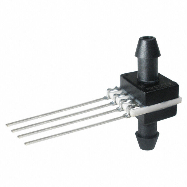
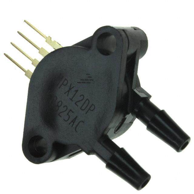
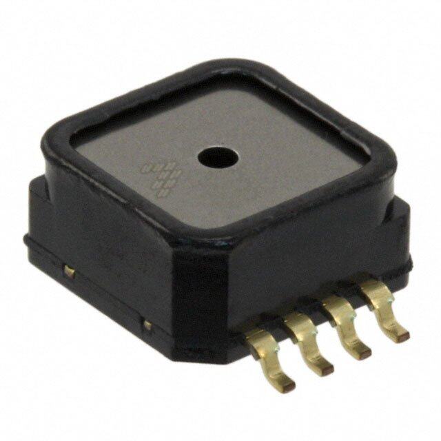
ICGOO电子元器件商城为您提供MPX12GP由Freescale Semiconductor设计生产,在icgoo商城现货销售,并且可以通过原厂、代理商等渠道进行代购。 MPX12GP价格参考¥56.07-¥85.99。Freescale SemiconductorMPX12GP封装/规格:压力传感器,变送器, 排气式压力计 压力 传感器 1.45 PSI(10 kPa) 公型 - 0.19"(4.93mm) 管 0 mV ~ 55 mV(3V) 4-SIP 模块。您可以下载MPX12GP参考资料、Datasheet数据手册功能说明书,资料中有MPX12GP 详细功能的应用电路图电压和使用方法及教程。
| 参数 | 数值 |
| 产品目录 | |
| 描述 | SENSOR GAUGE PRESS 1.45PSI MAX板机接口压力传感器 PRES SEN UNCOMP 12KPA |
| 产品分类 | |
| 品牌 | Freescale Semiconductor |
| 产品手册 | |
| 产品图片 |
|
| rohs | 符合RoHS无铅 / 符合限制有害物质指令(RoHS)规范要求 |
| 产品系列 | 板机接口压力传感器,Freescale Semiconductor MPX12GPMPX12 |
| 数据手册 | |
| 产品型号 | MPX12GP |
| 产品目录绘图 |
|
| 产品目录页面 | |
| 产品种类 | 板机接口压力传感器 |
| 出厂设置 | - |
| 单位重量 | 3.183 g |
| 压力类型 | Gauge |
| 商标 | Freescale Semiconductor |
| 安装风格 | Through Hole |
| 封装 | Tray |
| 封装/外壳 | 4-SIP 模块 |
| 封装/箱体 | Unibody 4-pin |
| 工作压力 | 1.45 psi |
| 工作温度 | -40°C ~ 125°C |
| 工作电源电压 | 3 V |
| 工厂包装数量 | 100 |
| 最大工作温度 | + 125 C |
| 最小工作温度 | - 40 C |
| 标准包装 | 600 |
| 电压-电源 | 3V |
| 端口大小 | 4.93 mm |
| 端口尺寸 | 公型,0.194"(4.9276mm)管 |
| 端口类型 | Single Radial Barbless |
| 端子类型 | PCB |
| 精度 | - |
| 系列 | MPXx12 |
| 输出 | 0 mV ~ 55 mV |


- 商务部:美国ITC正式对集成电路等产品启动337调查
- 曝三星4nm工艺存在良率问题 高通将骁龙8 Gen1或转产台积电
- 太阳诱电将投资9.5亿元在常州建新厂生产MLCC 预计2023年完工
- 英特尔发布欧洲新工厂建设计划 深化IDM 2.0 战略
- 台积电先进制程称霸业界 有大客户加持明年业绩稳了
- 达到5530亿美元!SIA预计今年全球半导体销售额将创下新高
- 英特尔拟将自动驾驶子公司Mobileye上市 估值或超500亿美元
- 三星加码芯片和SET,合并消费电子和移动部门,撤换高东真等 CEO
- 三星电子宣布重大人事变动 还合并消费电子和移动部门
- 海关总署:前11个月进口集成电路产品价值2.52万亿元 增长14.8%


PDF Datasheet 数据手册内容提取
Pressure Freescale Semiconductor MPX12 Rev 11, 07/2009 10 kPa Uncompensated MPX12 Silicon Pressure Sensors Series The MPX12 series silicon piezoresistive pressure sensors provide a very 0 to 10 kPa (0 to 1.45 psi) accurate and linear voltage output, directly proportional to the applied 55 mV Full Scale Span pressure. This standard, low cost, uncompensated sensor permits (Typical) manufacturers to design and add their own external temperature compensating and signal conditioning networks. Compensation techniques are simplified because of the predictability of Freescale's single element Application Examples strain gauge design. • Air Movement Control Features • Environmental Control Systems • Level Indicators • Low Cost • Leak Detection • Patented Silicon Shear Stress Strain Gauge Design • Medical Instrumentation • Ratiometric to Supply Voltage • Industrial Controls • Easy to Use Chip Carrier Package Options • Pneumatic Control Systems • Gauge Options • Robotics • Durable Epoxy Package ORDERING INFORMATION Package Case # of Ports Pressure Type Device Device Name Options No. None Single Dual Gauge Differential Absolute Marking Unibody Package (MPX12 Series) MPX12D Tray 344 • • MPX12D MPX12DP Tray 344C • • MPX12DP MPX12GP Tray 344B • • MPX12GP Small Outline Package (MPXV12 Series) MPXV12DP Tray 1351 • • MPXV12DP MPXV12GP Tray 1369 • • MPXV12GP MPXV12GW6U Rail 1735 • • MPXV12GW MPXV12GW7U Rail 1560 • • MPXV12GW MPAK Package (MPXM12 Series) MPXM12GS Rail 1320A • • MPXM12GS MPXM12GST1 Tape & Reel 1320A • • MPXM12GS © Freescale Semiconductor, Inc., 2007-2009. All rights reserved.
Pressure UNIBODY PACKAGES MPX12D MPX12GP MPX12DP CASE 344-15 CASE 344B-01 CASE 344C-01 SMALL OUTLINE PACKAGES MPXV12DP MPXV12GP MPXV12GW6U MPXV12GW7U CASE 1351-01 CASE 1369-01 CASE 1735-02 CASE 1560-02 MPAK PACKAGE MPXM12GS/GST1 CASE 1320A-02 MPX12 Sensors 2 Freescale Semiconductor
Pressure Operating Characteristics Table1. Operating Characteristics (V = 3.0 Vdc, T = 25°C unless otherwise noted, P1 > P2) S A Characteristic Symbol Min Typ Max Unit Differential Pressure Range(1) P 0 — 10 kPa OP Supply Voltage(2) V — 3.0 6.0 Vdc S Supply Current I — 6.0 — mAdc o Full Scale Span(3) V 45 55 70 mV FSS Offset(4) V 0 20 35 mV off Sensitivity ΔV/ΔP — 5.5 — mV/kPa Linearity — –0.5 — 5.0 %V FSS Pressure Hysteresis(6) (0 to 10 kPa) — — ±0.1 — %V FSS Temperature Hysteresis (–40°C to +125°C) — — ±0.5 — %V FSS Temperature Coefficient of Full Scale Span TCV –0.22 — –0.16 %V /°C FSS FSS Temperature Coefficient of Offset TCV — ±15 — μV/°C off Temperature Coefficient of Resistance TCR 0.21 — 0.27 %Z /°C in Input Impedance Z 400 — 550 Ω in Output Impedance Z 750 — 1250 Ω out Response Time(5) (10% to 90%) t — 1.0 — ms R Warm-Up Time(6) — — 20 — ms Offset Stability(7) — — ±0.5 — %V FSS 1. 1.0 kPa (kiloPascal) equals 0.145 psi. 2. Device is ratiometric within this specified excitation range. Operating the device above the specified excitation range may induce additional error due to device self-heating. 3. Full Scale Span (V ) is defined as the algebraic difference between the output voltage at full rated pressure and the output voltage at the FSS minimum related pressure. 4. Offset (V ) is defined as the output voltage at the minimum rated pressure. OFF 5. Response Time is defined as the time form the incremental change in the output to go from 10% to 90% of its final value when subjected to a specified step change in pressure. 6. Warm-up Time is defined as the time required for the product to meet the specified output voltage after the pressure is stabilized. 7. Offset stability is the product’s output deviation when subjected to 1000 hours of Pulsed Pressure, Temperature Cycling with Bias Test. MPX12 Sensors Freescale Semiconductor 3
Pressure Maximum Ratings Table2. Maximum Ratings(1) Rating Symbol Value Unit Maximum Pressure (P1 > P2) P 75 kPa MAX Burst Pressure (P1 > P2) P 100 kPa BURST Storage Temperature T –40 to +125 °C STG Operating Temperature T –40 to +125 °C A 1. Exposure beyond the specified limits may cause permanent damage or degradation to the device. Figure1 shows a block diagram of the internal circuitry integrated on a pressure sensor chip. 3 +V S 2 +V OUT Sensing Element 4 –V OUT 1 GND Figure1. Uncompensated Pressure Sensor Schematic Voltage Output versus Applied Differential Pressure The output voltage of the differential or gauge sensor voltage increases as increasing vacuum is applied to the increases with increasing pressure applied to the pressure vacuum side (P2) relative to the pressure side (P1). side (P1) relative to the vacuum side (P2). Similarly, output MPX12 Sensors 4 Freescale Semiconductor
Pressure Temperature Compensation Figure2 shows the typical output characteristics of the LINEARITY MPX12 series over temperature. Linearity refers to how well a transducer's output follows Because this strain gauge is an integral part of the silicon the equation: V = V + sensitivity x P over the operating OUT OFF diaphragm, there are no temperature effects due to pressure range (Figure3). There are two basic methods for differences in the thermal expansion of the strain gauge and calculating nonlinearity: (1) end point straight line fit or (2) a the diaphragm, as are often encountered in bonded strain least squares best line fit. While a least squares fit gives the gauge pressure sensors. However, the properties of the “best case” linearity error (lower numerical value), the strain gauge itself are temperature dependent, requiring that calculations required are burdensome. the device be temperature compensated if it is to be used Conversely, an end point fit will give the “worst case” error over an extensive temperature range. (often more desirable in error budget calculations) and the Temperature compensation and offset calibration can be calculations are more straightforward for the user. achieved rather simply with additional resistive components, or Freescale’s specified pressure sensor linearities are based by designing your system using the MPX2010D series sensor. on the end point straight line method measured at the Several approaches to external temperature midrange pressure. compensation over both –40 to +125°C and 0 to +80°C ranges are presented in Applications Note AN840. 80 V = 3 V +25°C 70 S DC P1 > P2 -40°C 60 Span c) 50 Range d V (Typ) m ut ( 40 +125°C p ut 30 O 20 10 Offset (Typ) 0 PSI 0 0.3 0.6 0.9 1.2 1.5 kPa 2.0 4.0 6.0 8.0 10 Pressure Differential Figure2. Output vs. Pressure Differential 80 Linearity 70 60 Actual 50 Span (V ) c) FSS Vd 40 m put ( 30 Theoretical ut O 20 Offset 10 (V ) OFF 0 0 Max P Pressure (kPa) OP Figure3. Linearity Specification Comparison MPX12 Sensors Freescale Semiconductor 5
Pressure Stainless Gel Die Coat Die Steel Cap P1 Thermoplastic Wire Bond Case Lead Frame P2 Differential Sensing Die Bond Element Figure4. Cross-Sectional Diagram (not to scale) Figure4 illustrates the differential/gauge die. A gel isolates pressure media. Media other than dry clean air may have the die surface and wire bonds from the environment, while adverse effects on sensor performance and long term allowing the pressure signal to be transmitted to the silicon reliability. Contact the factory for information regarding media diaphragm. compatibility in your application. Operating characteristics, internal reliability and qualification tests are based on use of dry clean air as the PRESSURE (P1)/VACUUM (P2) SIDE IDENTIFICATION TABLE Freescale designates the two sides of the pressure sensor Pressure (P1) Side as the Pressure (P1) side and the Vacuum (P2) side. The Part Number Case Type Identifier Pressure (P1) side is the side containing gel which isolates the die from the environment. Freescale’s MPx12 series is MPX12D 344 Stainless Steel Cap designed to operate with positive differential pressure MPX12DP 344C Side with Part Marking applied, P1 > P2. MPX12GP 344B Side with Port Attached The Pressure (P1) side may be identified by using the following table MPXV12DP 1351 Side with Part Marking MPXV12GP 1369 Side with Port MPXV12GW6U 1735 Side with Port MPXV12GW7U 1560 Side with Port MPXM12GS/GST1 1320A Side with Port Attached MPX12 Sensors 6 Freescale Semiconductor
Pressure PACKAGE DIMENSIONS NOTES: C 1. DIMENSIONING AND TOLERANCING PER ASME Y14.5M, 1994. R 2. CONTROLLING DIMENSION: INCH. 3. DIMENSION –A– IS INCLUSIVE OF THE MOLD STOP RING. MOLD STOP RING NOT TO EXCEED M 16.00 (0.630). Z 1 4 B –A– 2 3 INCHES MILLIMETERS DIM MIN MAX MIN MAX A 0.595 0.630 15.11 16.00 N B 0.514 0.534 13.06 13.56 PIN 1 1 2 3 4 L C 0.200 0.220 5.08 5.59 D 0.016 0.020 0.41 0.51 –T– F 0.048 0.064 1.22 1.63 SEATING G 0.100 BSC 2.54 BSC PLANE F J 0.014 0.016 0.36 0.40 J F G Y ML 0.63905 (cid:0) NO0M.725 17.3605 (cid:0) NO1M8.42 D 4 PL N 0.475 0.495 12.07 12.57 0.136 (0.005) M T A M DAMBAR TRIM ZONE: R 0.430 0.450 10.92 11.43 THIS IS INCLUDED Y 0.048 0.052 1.22 1.32 WITHIN DIM. “F” 8 PL Z 0.106 0.118 2.68 3.00 STYLE 1: STYLE 2: STYLE 3: PIN 1.GROUND PIN 1.VCC PIN 1.GND 2.+ OUTPUT 2.– SUPPLY 2.–VOUT 3.+ SUPPLY 3.+ SUPPLY 3.VS 4.– OUTPUT 4.GROUND 4.+VOUT CASE 344-15 ISSUE AA UNIBODY PACKAGE (cid:12)(cid:16)(cid:3)(cid:6)(cid:2)(cid:9) (cid:2)(cid:3)(cid:4)(cid:5)(cid:6)(cid:7)(cid:8) –T– –A– (cid:8)(cid:13)(cid:18)(cid:11)(cid:25)(cid:6)(cid:12)(cid:2)(cid:11)(cid:16)(cid:12)(cid:11)(cid:12)(cid:14)(cid:7)(cid:30)(cid:12)(cid:18)(cid:7)(cid:3)(cid:16)(cid:5)(cid:6)(cid:15)(cid:30)(cid:12)(cid:31)(cid:11)(cid:12)(cid:14)(cid:7)(cid:10)(cid:6)(cid:15)(cid:7)(cid:30)(cid:12)(cid:2)(cid:11) (cid:9)(cid:10)(cid:4)(cid:7)(cid:3) U (cid:4)(cid:8)(cid:22)(cid:13)(cid:27) (cid:7)(cid:8)!"(cid:19)(cid:13) (cid:19)(cid:13)(cid:31)(cid:16)(cid:12)(cid:3)(cid:15)(cid:16)(cid:5)(cid:5)(cid:11)(cid:12)(cid:14)(cid:7)(cid:18)(cid:11)(cid:25)(cid:6)(cid:12)(cid:2)(cid:11)(cid:16)(cid:12)(cid:9)(cid:7)(cid:11)(cid:12)(cid:31)#(cid:13) R L H (cid:6)(cid:7)(cid:19)(cid:20)(cid:3)(cid:2) (cid:16)(cid:6)(cid:10)(cid:10)(cid:6)(cid:16)(cid:3)(cid:5)(cid:3)(cid:18)(cid:2) (cid:15)(cid:6)(cid:16) (cid:16)(cid:6)(cid:7) (cid:16)(cid:4)(cid:17) (cid:16)(cid:6)(cid:7) (cid:16)(cid:4)(cid:17) (cid:4) (cid:8)(cid:13)(cid:8)(cid:22)(cid:27) (cid:8)(cid:13)(cid:8)$(cid:27) (cid:19)!(cid:13)(cid:26)" (cid:19)!(cid:13)"(cid:27) N (cid:21) (cid:26)(cid:13)%"(cid:27) (cid:26)(cid:13)$(cid:8)(cid:27) (cid:8)$(cid:13)(cid:22)(cid:26) (cid:8)"(cid:13)(cid:8)% PORT #1 POSITIVE –Q– (cid:19) (cid:26)(cid:13)(cid:21)(cid:26)(cid:27) (cid:26)(cid:13)(cid:21)(cid:19)(cid:27) $(cid:13)$(cid:27) "(cid:13)(cid:19)% PRESSURE (cid:15) (cid:26)(cid:13)(cid:26)(cid:8)% (cid:26)(cid:13)(cid:26)(cid:19)(cid:26) (cid:26)(cid:13)(cid:22)(cid:8) (cid:26)(cid:13)(cid:27)(cid:8) (P1) (cid:22) (cid:26)(cid:13)(cid:26)(cid:22)" (cid:26)(cid:13)(cid:26)%(cid:22) (cid:8)(cid:13)(cid:19)(cid:19) (cid:8)(cid:13)%(cid:21) (cid:8) (cid:26)(cid:13)(cid:8)(cid:26)(cid:26)(cid:7)&(cid:2)(cid:31) (cid:19)(cid:13)(cid:27)(cid:22)(cid:7)&(cid:2)(cid:31) (cid:20) (cid:26)(cid:13)(cid:8)"(cid:19) (cid:26)(cid:13)(cid:8)!(cid:22) (cid:22)(cid:13)%(cid:19) (cid:22)(cid:13)!(cid:21) B (cid:23) (cid:26)(cid:13)(cid:26)(cid:8)(cid:22) (cid:26)(cid:13)(cid:26)(cid:8)% (cid:26)(cid:13)(cid:21)% (cid:26)(cid:13)(cid:22)(cid:8) (cid:24) (cid:26)(cid:13)%!(cid:27) (cid:26)(cid:13)$(cid:19)(cid:27) (cid:8)$(cid:13)%(cid:27) (cid:8)"(cid:13)(cid:22)(cid:19) (cid:11) (cid:12) (cid:13) (cid:14) (cid:10) (cid:26)(cid:13)(cid:19)!(cid:26) (cid:26)(cid:13)(cid:21)(cid:26)(cid:26) $(cid:13)(cid:21)$ $(cid:13)%(cid:19) PIN 1 K (cid:7) (cid:26)(cid:13)(cid:22)(cid:19)(cid:26) (cid:26)(cid:13)(cid:22)(cid:22)(cid:26) (cid:8)(cid:26)(cid:13)%$ (cid:8)(cid:8)(cid:13)(cid:8)" –P– (cid:9) (cid:26)(cid:13)(cid:8)(cid:27)(cid:21) (cid:26)(cid:13)(cid:8)(cid:27)! (cid:21)(cid:13)"! (cid:22)(cid:13)(cid:26)(cid:22) (cid:25) (cid:26)(cid:13)(cid:8)(cid:27)(cid:21) (cid:26)(cid:13)(cid:8)(cid:27)! (cid:21)(cid:13)"! (cid:22)(cid:13)(cid:26)(cid:22) (cid:26)(cid:13)(cid:19)(cid:27)(cid:7)(cid:28)(cid:26)(cid:13)(cid:26)(cid:8)(cid:26)(cid:29)(cid:25) (cid:3) (cid:24) (cid:2) S (cid:18) (cid:26)(cid:13)(cid:19)(cid:21)(cid:26) (cid:26)(cid:13)(cid:19)(cid:27)(cid:26) (cid:27)(cid:13)"(cid:22) %(cid:13)(cid:21)(cid:27) (cid:2) (cid:26)(cid:13)(cid:19)(cid:19)(cid:26) (cid:26)(cid:13)(cid:19)(cid:22)(cid:26) (cid:27)(cid:13)(cid:27)! %(cid:13)(cid:8)(cid:26) J F (cid:26) (cid:26)(cid:13)!(cid:8)(cid:26)(cid:7)&(cid:2)(cid:31) (cid:19)(cid:21)(cid:13)(cid:8)(cid:8)(cid:7)&(cid:2)(cid:31) C G D4 PL (cid:26)(cid:13)(cid:8)(cid:21)(cid:7)(cid:28)(cid:26)(cid:13)(cid:26)(cid:26)(cid:27)(cid:29)(cid:25) (cid:3) (cid:2) (cid:2) (cid:24) (cid:2) (cid:2)(cid:3)(cid:4)(cid:5)(cid:6)(cid:7)(cid:8)(cid:9) (cid:10)(cid:11)(cid:12)(cid:7)(cid:8)(cid:13)(cid:14)(cid:15)(cid:16)(cid:17)(cid:12)(cid:18) (cid:19)(cid:13)(cid:20)(cid:7)(cid:16)(cid:17)(cid:3)(cid:10)(cid:17)(cid:3) (cid:21)(cid:13)(cid:20)(cid:7)(cid:2)(cid:17)(cid:10)(cid:10)(cid:5)(cid:4) (cid:22)(cid:13)(cid:23)(cid:7)(cid:16)(cid:17)(cid:3)(cid:10)(cid:17)(cid:3) CASE 344B-01 ISSUE B UNIBODY PACKAGE MPX12 Sensors Freescale Semiconductor 7
Pressure PACKAGE DIMENSIONS –A– NOTES: V 1.DIMENSIONING AND TOLERANCING PER ANSI U Y14.5M, 1982. R PORT #1 W L 2.CONTROLLING DIMENSION: INCH. H INCHES MILLIMETERS PORT #2 PORT #2 PORT #1 DIM MIN MAX MIN MAX N VA(CPU2U)M P(PO1S)ITIVE PRESSURE AB 10..164855 10..177155 2197..0480 2198..8156 –Q– C 0.405 0.435 10.29 11.05 D 0.016 0.020 0.41 0.51 F 0.048 0.064 1.22 1.63 SEATING B SEATING G 0.100 BSC 2.54 BSC PLANE PLANE H 0.182 0.194 4.62 4.93 J 0.014 0.016 0.36 0.41 PIN 1 1 2 3 4 K 0.695 0.725 17.65 18.42 K –P– L 0.290 0.300 7.37 7.62 N 0.420 0.440 10.67 11.18 –T– –T– 0.25 (0.010) M T Q S S P 0.153 0.159 3.89 4.04 Q 0.153 0.159 3.89 4.04 J F R 0.063 0.083 1.60 2.11 C G S 0.220 0.240 5.59 6.10 D 4 PL U 0.910 BSC 23.11 BSC V 0.248 0.278 6.30 7.06 0.13 (0.005) M T S S Q S W 0.310 0.330 7.87 8.38 STYLE 1: PIN 1.GROUND 2.+ OUTPUT 3.+ SUPPLY 4.– OUTPUT CASE 344C-01 ISSUE B UNIBODY PACKAGE MPX12 Sensors 8 Freescale Semiconductor
Pressure PACKAGE DIMENSIONS CASE 1351-01 ISSUE A SMALL OUTLINE PACKAGE MPX12 Sensors Freescale Semiconductor 9
Pressure PACKAGE DIMENSIONS CASE 1351-01 ISSUE A SMALL OUTLINE PACKAGE MPX12 Sensors 10 Freescale Semiconductor
Pressure PACKAGE DIMENSIONS 2 PLACES 4 TIPS 0.008 (0.20) C A B A E e GAGE PLANE 5 4 e/2 .014 (0.35) θ L A1 D DETAIL G 8 1 NOTES: 1. CONTROLLING DIMENSION: INCH. 8X b 2. INTERPRET DIMENSIONS AND TOLERANCES PER F 0.004 (0.1) M C A B ASME Y14.5M, 1994. 3. DIMENSIONS "D" AND "E1" DO NOT INCLUDE MOLD FLASH OR PROTRUSIONS. MOLD FLASH OR PROTRUSIONS SHALL NOT EXCEED 0.006 (0.152) B E1 PER SIDE. 4. DIMENSION "b" DOES NOT INCLUDE DAMBAR PROTRUSION. ALLOWABLE DAMBAR PROTRUSION SHALL BE 0.008 (0.203) MAXIMUM. INCHES MILLIMETERS ∅T N K DAIM 0M.3I0N0 M0.3A3X0 M7.1IN1 M7.A62X A1 0.002 0.010 0.05 0.25 b 0.038 0.042 0.96 1.07 D 0.465 0.485 11.81 12.32 E 0.717 BSC 18.21 BSC A M Ee1 0.406.1500 B0S.C485 11.821.54 BS1C2.32 F 0.245 0.255 6.22 6.47 K 0.120 0.130 3.05 3.30 8X 0.004 (0.1) L 0.061 0.071 1.55 1.80 P M 0.270 0.290 6.86 7.36 DETAIL G N 0.080 0.090 2.03 2.28 P 0.009 0.011 0.23 0.28 C SEATING T 0.115 0.125 2.92 3.17 PLANE θ 0˚ 7˚ 0˚ 7˚ CASE 1369-01 ISSUE O SMALL OUTLINE PACKAGE MPX12 Sensors Freescale Semiconductor 11
Pressure PACKAGE DIMENSIONS CASE 1735-02 ISSUE B SMALL OUTLINE PACKAGE MPX12 Sensors 12 Freescale Semiconductor
Pressure PACKAGE DIMENSIONS CASE 1735-02 ISSUE B SMALL OUTLINE PACKAGE MPX12 Sensors Freescale Semiconductor 13
Pressure PACKAGE DIMENSIONS CASE 1735-02 ISSUE B SMALL OUTLINE PACKAGE MPX12 Sensors 14 Freescale Semiconductor
Pressure PACKAGE DIMENSIONS CASE 1560-03 ISSUE D SMALL OUTLINE PACKAGE MPX12 Sensors Freescale Semiconductor 15
Pressure PACKAGE DIMENSIONS CASE 1560-03 ISSUE D SMALL OUTLINE PACKAGE MPX12 Sensors 16 Freescale Semiconductor
Pressure PACKAGE DIMENSIONS CASE 1560-03 ISSUE D SMALL OUTLINE PACKAGE MPX12 Sensors Freescale Semiconductor 17
Pressure PACKAGE DIMENSIONS CASE 1320A-02 ISSUE A MPAK PACKAGE MPX12 Sensors 18 Freescale Semiconductor
Pressure PACKAGE DIMENSIONS CASE 1320A-02 ISSUE A MPAK PACKAGE MPX12 Sensors Freescale Semiconductor 19
How to Reach Us: Home Page: www.freescale.com Web Support: http://www.freescale.com/support USA/Europe or Locations Not Listed: Freescale Semiconductor, Inc. Technical Information Center, EL516 2100 East Elliot Road Tempe, Arizona 85284 1-800-521-6274 or +1-480-768-2130 www.freescale.com/support Europe, Middle East, and Africa: Information in this document is provided solely to enable system and software Freescale Halbleiter Deutschland GmbH Technical Information Center implementers to use Freescale Semiconductor products. There are no express or Schatzbogen 7 implied copyright licenses granted hereunder to design or fabricate any integrated 81829 Muenchen, Germany circuits or integrated circuits based on the information in this document. +44 1296 380 456 (English) +46 8 52200080 (English) +49 89 92103 559 (German) Freescale Semiconductor reserves the right to make changes without further notice to +33 1 69 35 48 48 (French) any products herein. Freescale Semiconductor makes no warranty, representation or www.freescale.com/support guarantee regarding the suitability of its products for any particular purpose, nor does Freescale Semiconductor assume any liability arising out of the application or use of any Japan: product or circuit, and specifically disclaims any and all liability, including without Freescale Semiconductor Japan Ltd. limitation consequential or incidental damages. “Typical” parameters that may be Headquarters provided in Freescale Semiconductor data sheets and/or specifications can and do vary ARCO Tower 15F in different applications and actual performance may vary over time. All operating 1-8-1, Shimo-Meguro, Meguro-ku, parameters, including “Typicals”, must be validated for each customer application by Tokyo 153-0064 Japan customer’s technical experts. Freescale Semiconductor does not convey any license 0120 191014 or +81 3 5437 9125 under its patent rights nor the rights of others. Freescale Semiconductor products are support.japan@freescale.com not designed, intended, or authorized for use as components in systems intended for surgical implant into the body, or other applications intended to support or sustain life, Asia/Pacific: or for any other application in which the failure of the Freescale Semiconductor product Freescale Semiconductor China Ltd. could create a situation where personal injury or death may occur. Should Buyer Exchange Building 23F purchase or use Freescale Semiconductor products for any such unintended or No. 118 Jianguo Road unauthorized application, Buyer shall indemnify and hold Freescale Semiconductor and Chaoyang District its officers, employees, subsidiaries, affiliates, and distributors harmless against all Beijing 100022 China claims, costs, damages, and expenses, and reasonable attorney fees arising out of, +86 010 5879 8000 directly or indirectly, any claim of personal injury or death associated with such support.asia@freescale.com unintended or unauthorized use, even if such claim alleges that Freescale Semiconductor was negligent regarding the design or manufacture of the part. For Literature Requests Only: Freescale Semiconductor Literature Distribution Center 1-800-441-2447 or +1-303-675-2140 Freescale™ and the Freescale logo are trademarks of Freescale Semiconductor, Inc. Fax: +1-303-675-2150 All other product or service names are the property of their respective owners. LDCForFreescaleSemiconductor@hibbertgroup.com © Freescale Semiconductor, Inc. 2009. All rights reserved. MPX12 Rev. 11 07/2009