
 Datasheet下载
- 型号: MPL3115A2
- 制造商: Freescale Semiconductor
- 库位|库存: xxxx|xxxx
- 要求:
| 数量阶梯 | 香港交货 | 国内含税 |
| +xxxx | $xxxx | ¥xxxx |
查看当月历史价格
查看今年历史价格
MPL3115A2产品简介:
ICGOO电子元器件商城为您提供MPL3115A2由Freescale Semiconductor设计生产,在icgoo商城现货销售,并且可以通过原厂、代理商等渠道进行代购。 MPL3115A2价格参考。Freescale SemiconductorMPL3115A2封装/规格:压力传感器,变送器, 绝对 压力 传感器 7.25 PSI ~ 15.95 PSI(50 kPa ~ 110 kPa) 24 b 8-TLGA。您可以下载MPL3115A2参考资料、Datasheet数据手册功能说明书,资料中有MPL3115A2 详细功能的应用电路图电压和使用方法及教程。
| 参数 | 数值 |
| 产品目录 | |
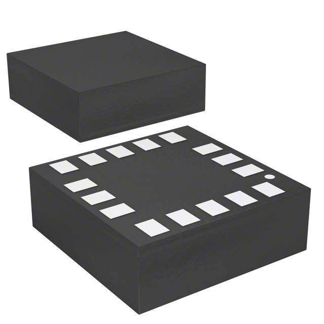
| 描述 | IC ALTIMETER I2C VERSION 8LGA板机接口压力传感器 I 2 C VERSION |
| 产品分类 | |
| 品牌 | Freescale Semiconductor |
| 产品手册 | |
| 产品图片 |
|
| rohs | 符合RoHS无铅 / 符合限制有害物质指令(RoHS)规范要求 |
| 产品系列 | 板机接口压力传感器,Freescale Semiconductor MPL3115A2- |
| 数据手册 | |
| 产品型号 | MPL3115A2 |
| 产品种类 | 板机接口压力传感器 |
| 准确性 | +/- 0.4 KPa |
| 出厂设置 | - |
| 单位重量 | 31.300 mg |
| 压力类型 | Absolute |
| 商标 | Freescale Semiconductor |
| 安装风格 | SMD/SMT |
| 封装 | Tray |
| 封装/外壳 | 8-TLGA |
| 封装/箱体 | LGA-8 |
| 工作压力 | 20 kPa to 110 kPa |
| 工作温度 | -40°C ~ 85°C |
| 工作电源电压 | 2.5 V |
| 工厂包装数量 | 490 |
| 最大工作温度 | + 85 C |
| 最小工作温度 | - 40 C |
| 标准包装 | 1,960 |
| 电压-电源 | 1.95 V ~ 3.6 V |
| 电源电压-最大 | 3.6 V |
| 电源电压-最小 | 1.95 V |
| 电源电流 | 2 uA |
| 端口尺寸 | - |
| 端口类型 | No Ports |
| 端子类型 | PCB |
| 精度 | ±400Pa |
| 输出 | 数字,I²S |
| 输出类型 | Digital |
| 配用 | /product-detail/zh/1893/1528-1034-ND/4990783 |


- 商务部:美国ITC正式对集成电路等产品启动337调查
- 曝三星4nm工艺存在良率问题 高通将骁龙8 Gen1或转产台积电
- 太阳诱电将投资9.5亿元在常州建新厂生产MLCC 预计2023年完工
- 英特尔发布欧洲新工厂建设计划 深化IDM 2.0 战略
- 台积电先进制程称霸业界 有大客户加持明年业绩稳了
- 达到5530亿美元!SIA预计今年全球半导体销售额将创下新高
- 英特尔拟将自动驾驶子公司Mobileye上市 估值或超500亿美元
- 三星加码芯片和SET,合并消费电子和移动部门,撤换高东真等 CEO
- 三星电子宣布重大人事变动 还合并消费电子和移动部门
- 海关总署:前11个月进口集成电路产品价值2.52万亿元 增长14.8%
PDF Datasheet 数据手册内容提取
MPL3115A2 2 I C precision pressure sensor with altimetry Rev. 7 — 15 February 2018 Data sheet: technical data 1 General description 2 The MPL3115A2 is a compact, piezoresistive, absolute pressure sensor with an I C digital interface. MPL3115A2 has a wide operating range of 20 kPa to 110 kPa, a range that covers all surface elevations on earth. The MEMS is temperature compensated utilizing an on-chip temperature sensor. The pressure and temperature data is fed into a high resolution ADC to provide fully compensated and digitized outputs for pressure in Pascals and temperature in °C. The compensated pressure output can then be converted to altitude, utilizing the formula stated in Section 9.1.3 "Pressure/altitude" provided in meters.The internal processing in MPL3115A2 removes compensation and unit conversion load from the system MCU, simplifying system design. MPL3115A2's advanced ASIC has multiple user programmable modes such as power saving, interrupt and autonomous data acquisition modes, including programmed acquisition cycle timing, and poll-only modes. Typical active supply current is 40 μA per measurement-second for a stable 10 cm output resolution. 2 Features and benefits • Operating range: 20 kPa to 110 kPa absolute pressure • Programmable interrupts • Calibrated range: 50 kPa to 110 kPa absolute pressure • Autonomous data acquisition • Calibrated temperature output: −40 °C to 85 °C – Embedded 32-sample FIFO 2 • I C digital output interface – Data logging up to 12 days using the FIFO • Fully compensated internally – One-second to nine-hour data acquisition rate • Precision ADC resulting in 0.1 meter of effective resolution • 1.95 V to 3.6 V supply voltage, internally regulated • Direct reading • 1.6 V to 3.6 V digital interface supply voltage – Pressure: 20-bit measurement (Pascals) • Operating temperature from −40 °C to +85 °C – 20 to 110 kPa – Altitude: 20-bit measurement (meters) – –698 to 11,775 m – Temperature: 12-bit measurement (°C) – –40 °C to 85 °C
NXP Semiconductors MPL3115A2 2 I C precision pressure sensor with altimetry 3 Applications • High-accuracy altimetry and barometry • Smartphones, tablets and wearable devices • GPS applications: dead reckoning, map assist, navigation, enhancement for emergency services • Weather station equipment 4 Ordering information Table 1. Ordering information Device number Shipping Package Number of ports Pressure Type Digital interface None Single Dual Gauge Differential Absolute MPL3115A2 Tray 98ASA002260D ● — — — — ● ● MPL3115A2R1 Tape and reel 98ASA002260D ● — — — — ● ● 5 Block diagram Figure 1. Block diagram MPL3115A2 All information provided in this document is subject to legal disclaimers. © NXP B.V. 2018. All rights reserved. Data sheet: technical data Rev. 7 — 15 February 2018 2 / 52
NXP Semiconductors MPL3115A2 2 I C precision pressure sensor with altimetry 6 Pinning information 6.1 Pinning MPL3115A2 V 1 8 SCL DD CAP 2 7 SDL GND 3 6 INT1 V 4 5 INT2 DDIO Transparent top view Figure 2. 8-pin LGA pinout 6.2 Pin description Table 2. Pin description Symbol Pin Description V 1 V power supply connection (1.95 to 3.6 V) DD DD CAP 2 External capacitor GND 3 Ground V 4 Digital interface power supply (1.62 to 3.6 V) DDIO INT2 5 Pressure interrupt 2 INT1 6 Pressure interrupt 1 2 SDL 7 I C serial data 2 SCL 8 I C serial clock 7 System connections V DD 1 8 SCL 100nF 10μF 2 7 SDL 100nF 3 6 INT1 MPL3115A2 V 4 5 INT2 DDIO Figure 3. Typical application diagram MPL3115A2 All information provided in this document is subject to legal disclaimers. © NXP B.V. 2018. All rights reserved. Data sheet: technical data Rev. 7 — 15 February 2018 3 / 52
NXP Semiconductors MPL3115A2 2 I C precision pressure sensor with altimetry The device power is supplied through the V line. Power supply decoupling capacitors DD (100 nF ceramic plus 10 μF bulk or 10 μF ceramic) should be placed as near as possible to pin 1 of the device. A second 100 nF capacitor is used to bypass the internal regulator. The functions, threshold and the timing of the interrupt pins (INT1 and INT2) are user 2 programmable through the I C interface. 8 Handling and board mount recommendations The sensor die is sensitive to light exposure. Direct light exposure through the port hole can lead to varied accuracy of pressure measurement. Avoid such exposure to the port during normal operation. 8.1 Methods of handling Components can be picked from the carrier tape using either the vacuum assist or the mechanical type pickup heads. A vacuum assist nozzle type is most common due to its lower cost of maintenance and ease of operation. The recommended vacuum nozzle configuration should be designed to make contact with the device directly on the metal cover and avoid vacuum port location directly over the vent hole in the metal cover of the device. Multiple vacuum ports within the nozzle may be required to effectively handle the device and prevent shifting during movement to placement position. Vacuum pressure required to adequately support the component should be approximately 25 in Hg (85kPa). This level is typical of in-house vacuum supply. Pickup nozzles are available in various sizes and configurations to suit a variety of component geometries. To select the nozzle best suited for the specific application, it is recommended that the customer consult their pick and place equipment supplier to determine the correct nozzle. In some cases it may be necessary to fabricate a special nozzle depending on the equipment and speed of operation. Tweezers or other mechanical forms of handling that have a sharp point are not recommended since they can inadvertently be inserted into the vent hole of the device. This can lead to a puncture of the MEMS element that will render the device inoperable. 8.2 Board mount recommendations Components can be mounted using solder paste stencil, screen printed or dispensed onto the PCB pads prior to placement of the component. The volume of solder paste applied to the PCB is normally sufficient to secure the component during transport to the subsequent reflow soldering process. Use of adhesives to secure the component is not recommended, but where necessary can be applied to the underside of the device. Solder pastes are available in variety of metal compositions, particle size and flux types. The solder paste consists of metals and flux required for a reliable connection between the component lead and the PCB pad. Flux aids the removal of oxides that may be present on PCB pads and prevents further oxidation from occurring during the solder process. The use of a No-Clean (NC) flux is recommended for exposed cavity components. Using pressure spray, wire brush, or other methods of cleaning is not recommended since it can puncture the MEMS device and render it unusable. If cleaning of the pcb is performed Water Soluble (WS) flux can be used. However, it is recommended the component cavity is protected by adhesive Kapton tape, vinyl cap or other means prior to the cleaning process. This covering will prevent damage to the MEMS device, MPL3115A2 All information provided in this document is subject to legal disclaimers. © NXP B.V. 2018. All rights reserved. Data sheet: technical data Rev. 7 — 15 February 2018 4 / 52
NXP Semiconductors MPL3115A2 2 I C precision pressure sensor with altimetry contamination, and foreign materials from being introduced into device cavity as result of cleaning processes. Ultrasonic cleaning is not recommended as the frequencies can damage wire bond interconnections and the MEMS device. 9 Mechanical and electrical specifications 9.1 Terminology 9.1.1 Resolution The resolution of a pressure sensor is the minimum change of pressure that can be reliably measured. The usable resolution of the device is programmable, enabling the user to choose a compromise between acquisition speed, power consumption, and resolution that best fits the application. To simplify the programming, the data is always reported in the same format with differing number of usable bits. 9.1.2 Accuracy 9.1.2.1 Offset The offset is defined as the output signal obtained when the reference pressure (a vacuum for an absolute pressure sensor) is applied to the sensor. Offset error affects absolute pressure measurements but not relative pressure measurements. An altitude measurement is the pressure value in comparison to sea level, a barometric measurement is the pressure value read by the sensor. That is, a measurement of total pressure seen (for example 70 kPa), or total height (for example 3000 m) above sea level. A change in the offset will affect the pressure value or height seen above sea level as it shifts the sea level base reference. An absolute pressure measurement is not the same as relative pressure measurement, where the pressure is compared when raising or lowering pressure in shorter intervals. This would be a walk up a hill, measuring the pressure and altitude difference from start to finish. In the relative case, the offset shifts are shared in the two absolute measurements and negate each other during the pressure calculation. For the MPL3115A2, the long term offset shift can be removed by adjusting the pressure or altitude offset correction. See Section 14.23 "Offset correction registers".This adjustment is provided to override the factory programmed values to compensate for offsets introduced by manufacturing and mounting stresses. It is highly recommended that this is utilized to realize the full accuracy potential of the device. 9.1.2.2 Linearity Linearity compares the slope of the measurement data to that of an ideal transfer function. It refers to how well a transducer's output follows the equation P = P + sensitivity × P straight-line equation over the operating pressure range. OUT OFF The method used by NXP to give the linearity specification is the end-point straight line method measured at midrange pressure. MPL3115A2 All information provided in this document is subject to legal disclaimers. © NXP B.V. 2018. All rights reserved. Data sheet: technical data Rev. 7 — 15 February 2018 5 / 52
NXP Semiconductors MPL3115A2 2 I C precision pressure sensor with altimetry 9.1.2.3 Absolute pressure Absolute pressure sensors measure an external pressure relative to a zero- pressure reference (vacuum) sealed inside the reference chamber of the die during manufacturing. This standard allows comparison to a standard value set such that 14.7 psi = 101,325 Pa = 1 atm at sea level as a measurement target. The absolute pressure is used to determine altitude as it has a constant reference for comparison. Measurement at sea level can be compared to measurement at a mountain summit as they use the same vacuum reference. The conversion of absolute pressure to altitude in meters is calculated based on US Standard Atmosphere 1976 (NASA). Note: Absolute pressure is not linear in relation to altitude, it is an exponential function. The value of altitude can be read directly from the device in increments of 0.0625 meters, or the value of pressure in 0.25 Pascal (Pa) units. 9.1.2.4 Span Span is the value of full-scale output with offset subtracted, representing the full range of the pressure sensor. Ideally the span is a specification over a constant temperature. The device uses internal temperature compensation to remove drift. Span accuracy is the comparison of the measured difference and the actual difference between the highest and lowest pressures in the specified range. 9.1.3 Pressure/altitude The device is a high accuracy pressure sensor with integrated data calculation and logging capabilities. To provide altitude readings, the altitude calculations are based on the measured pressure (p), the user input of the equivalent sea level pressure to compensate for local weather conditions (OFF_H) and the US Standard Atmosphere 1976 (NASA). Pressure is given in Pascals (Pa), and fractions of a Pa. Altitude is given in meters (m) and fractions of a meter. The altitude is calculated from the pressure using the following equation: where: p = sea level pressure (101,326 Pa) 0 h = altitude in meters 9.2 Absolute maximum ratings Absolute maximum ratings are the limits the device can be exposed to without permanently damaging it. Absolute maximum ratings are stress ratings only, functional operation at these ratings is not guaranteed. Exposure to absolute maximum ratings conditions for extended periods may affect device reliability. This device contains circuitry to protect against damage due to high static voltage or electrical fields. It is advised, however, that normal precautions be taken to avoid application of any voltages higher than maximum-rated voltages to this high-impedance circuit. MPL3115A2 All information provided in this document is subject to legal disclaimers. © NXP B.V. 2018. All rights reserved. Data sheet: technical data Rev. 7 — 15 February 2018 6 / 52
NXP Semiconductors MPL3115A2 2 I C precision pressure sensor with altimetry Table 3. Maximum ratings Symbol Characteristic Value Unit P Maximum applied pressure 500 kPa max V Supply voltage −0.3 to 3.6 V DD V Interface supply voltage −0.3 to 3.6 V DDIO V Input voltage on any control pin (SCL, SDA) −0.3 to V + 0.3 V IN DDIO T Operating temperature range −40 to +85 °C OP T Storage temperature range −40 to +125 °C STG Table 4. ESD and latchup protection characteristics Symbol Rating Value Unit HBM Human body model ±2000 V CDM Charge device model ±500 V — Latchup current at T = 85 °C ±100 mA Caution This device is sensitive to mechanical shock. Improper handling can cause permanent damage to the part or cause the part to otherwise fail. Caution This is an ESD sensitive device. Improper handling can cause permanent damage to the part. msc896 MPL3115A2 All information provided in this document is subject to legal disclaimers. © NXP B.V. 2018. All rights reserved. Data sheet: technical data Rev. 7 — 15 February 2018 7 / 52
NXP Semiconductors MPL3115A2 2 I C precision pressure sensor with altimetry 9.3 Mechanical characteristics Table 5. Mechanical characteristics V = 2.5 V, T = 25 °C, over 50 kPa to 110 kPa, unless otherwise noted. DD Symbol Parameter Test conditions Min Typ Max Unit Pressure sensor P Measurement range Calibrated range 50 –– 110 kPa FS Operational range 20 –– 110 kPa [1] Pressure reading noise 1x oversample –– 19 –– Pa RMS 128x oversample –– 1.5 –– Pa RMS Pressure absolute accuracy 50 to 110 kPa over 0 °C to 50 –0.4 –– 0.4 kPa °C 50 to 110 kPa over−10 °C to –– ±0.4 –– kPa 70 °C Pressure relative accuracy Relative accuracy during –– ±0.05 –– kPa pressure change between 70 to 110 kPa at any constant temperature between −10 °C to 50 °C Relative accuracy during –– ±0.1 –– kPa changing temperature between −10 °C to 50 °C at any constant pressure between 50 kPa to 110 kPa Pressure/altitude resolution Barometer mode 0.25 1.5 –– Pa [2][3][4] Altimeter mode 0.0625 0.3 –– m Output data rate One-shot mode –– 100 –– Hz FIFO mode –– –– 1 Hz Board mount drift After solder reflow –– ±0.15 –– kPa Long term drift After a period of 1 year –– ±0.1 –– kPa Temperature sensor T Measurement range –– –40 –– +85 °C FS Temperature accuracy @25 °C –– ±1 –– °C Over temperature range –– ±3 –– °C T Operating temperature –– –40 –– +85 °C OP range [1] Oversample (OSR) modes internally combine and average samples to reduce noise. [2] Smallest bit change in register represents minimum value change in Pascals or meters. Typical resolution to signify change in altitude is 0.3 m. [3] Reference pressure = 101.325 kPa (sea level). [4] At 128x oversample ratio. MPL3115A2 All information provided in this document is subject to legal disclaimers. © NXP B.V. 2018. All rights reserved. Data sheet: technical data Rev. 7 — 15 February 2018 8 / 52
NXP Semiconductors MPL3115A2 2 I C precision pressure sensor with altimetry 9.4 Electrical characteristics Table 6. Electrical characteristics @ V = 2.5 V, T = 25 °C unless otherwise noted. DD Symbol Parameter Test conditions Min Typ Max Unit V I/O supply voltage — 1.62 1.8 3.6 V DDIO V Operating supply voltage — 1.95 2.5 3.6 V DD I Integrated current 1 update Highest speed mode — 8.5 — µA DD per second oversample = 1 Standard mode oversample — 40 — µA = 16 High resolution mode — 265 — µA oversample = 128 I Max current during During acquisition/ — 2 — mA DDMAX acquisition and conversion conversion I Supply current drain in STANDBY mode selected — 2 — µA DDSTBY STANDBY mode SBYB = 0 VIH Digital high level input — 0.75 — — V DDIO voltage SCL, SDA VIL Digital low level input voltage — — — 0.3 V DDIO SCL, SDA VOH High level output voltage I = 500 µA 0.9 — — V O DDIO INT1, INT2 VOL Low level output voltage I = 500 µA — — 0.1 V O DDIO INT1, INT2 VOLS Low level output voltage I = 500 µA — — 0.1 V O DDIO SDA [1][2][3] T Turn-on time High speed mode — — 60 ms ON High resolution mode — — 1000 ms T Operating temperature range — −40 25 +85 °C OP 2 I C addressing 2 I C Address — — 0x60 Hex The device uses 7-bit addressing and does not acknowledge general call address 000 0000. Slave address has been set to 60h or 110 0000. 8-bit read is C1h, 8-bit write is C0h. [1] Time to obtain valid data from STANDBY mode to ACTIVE mode [2] High speed mode is achieved by setting the oversample rate of 1x. [3] High resolution mode is achieved by setting the oversample to 128x. MPL3115A2 All information provided in this document is subject to legal disclaimers. © NXP B.V. 2018. All rights reserved. Data sheet: technical data Rev. 7 — 15 February 2018 9 / 52
NXP Semiconductors MPL3115A2 2 I C precision pressure sensor with altimetry 10 Digital interface 2 The registers embedded inside the device are accessed through an I C serial interface. Table 7. Serial interface pin descriptions Name Description 2 SCL I C serial clock 2 SDA I C serial data 2 10.1 I C characteristics 2 Table 8. I C Slave timing values All values referred to VIH(min) and VIL(max) levels. 2 Symbol Parameter I C Unit Condition Min Max f SCL clock frequency Pull-up = 1 kΩ, Cb = 400 pF 0 400 kHz SCL f SCL clock frequency Pull-up = 1 kΩ, Cb = 20 pF 0 4 MHz SCL t Bus free time between STOP — 1.3 — µs BUF and START condition t Repeated START hold time — 0.6 — µs HD;STA t Repeated START setup time — 0.6 — µs SU;STA t STOP condition setup time — 0.6 — µs SU;STO [1][2][3] t SDA data hold time — 50 — ns HD;DAT [4] t SDA setup time — 100 — ns SU;DAT t SCL clock low time — 1.3 — µs LOW t SCL clock high time — 0.6 — µs HIGH [5] t SDA and SCL rise time — 20 + 0.1C 300 ns r b [2][5][6][7] t SDA and SCL fall Time — 20+ 0.1C 300 ns f b t Pulse width of spikes that are — — 50 ns SP suppressed by internal input filter [1] tHD;DAT is the data hold time that is measured from the falling edge of SCL, applies to data in transmission and the acknowledge. [2] The device must internally provide a hold time of at least 300 ns for the SDA signal (with respect to the VIH(min) of the SCL signal) to bridge the undefined region of the falling edge of SCL [3] The maximum tHD;DAT must be less than the maximum of tVD;DAT or tVD;ACK by a transition time. This device does not stretch the LOW period (tLOW) of the SCL signal. [4] A fast mode I2C device can be used in a standard mode I2C system, but the requirement tSU;DAT 250 ns must then be met. This will automatically be the case if the device does not stretch the LOW period of the SCL signal. If such a device does stretch the LOW period of the SCL signal, it must output the next data bit to the SDA line tr(max) + tSU;DAT = 1000 + 250 = 1250 ns (according to the standard mode I2C specification) before the SCL line is released. Also the acknowledge timing must meet this set-up time. [5] Cb = Total capacitance of one bus line in pF. [6] The maximum tf for the SDA and SCL bus lines is specified at 300 ns. The maximum fall time for the SDA output stage tf is specified at 250 ns. This allows series protection resistors to be connected in between the SDA and the SCL pins and the SDA/SCL bus lines without exceeding the maximum specified tf. [7] In fast mode plus, fall time is specified the same for both output stage and bus timing. If series resistors are used, designers should allow for this when considering bus timing. MPL3115A2 All information provided in this document is subject to legal disclaimers. © NXP B.V. 2018. All rights reserved. Data sheet: technical data Rev. 7 — 15 February 2018 10 / 52
NXP Semiconductors MPL3115A2 2 I C precision pressure sensor with altimetry 2 10.2 I C operation The transaction on the bus is started through a start condition (START) signal. START condition is defined as a HIGH to LOW transition on the data line while the SCL line is held HIGH. After START has been transmitted by the master, the bus is considered busy. The next byte of data transmitted after START contains the slave address in the first 7 bits, and the eighth bit tells whether the master is receiving data from the slave or transmitting data to the slave. When an address is sent, each device in the system compares the first seven bits after a start condition with its address. If they match, the device considers itself addressed by the master. The ninth clock pulse, following the slave address byte (and each subsequent byte) is the acknowledge (ACK).The transmitter must release the SDA line during the ACK period. The receiver must then pull the data line low so that it remains stable low during the high period of the acknowledge clock period. The number of bytes per transfer is unlimited. If the master cannot receive another complete byte of data until it has performed some other function, it can hold the clock line, SCL low to force the transmitter into a wait state. Data transfer only continues when the master is ready for another byte and releases the clock line. A low to high transition on the SDA line while the SCL line is high is defined as a stop condition (STOP). A data transfer is always terminated by a STOP. A master may also issue a repeated START during a data transfer. Device expects repeated STARTs to be used to randomly read from specific registers. 2 The standard 7-bit I C slave address is 60h or 1100000. 8-bit read is C1h, 8-bit write is C0h. 2 Figure 4. I C slave timing diagram MPL3115A2 All information provided in this document is subject to legal disclaimers. © NXP B.V. 2018. All rights reserved. Data sheet: technical data Rev. 7 — 15 February 2018 11 / 52
NXP Semiconductors MPL3115A2 2 I C precision pressure sensor with altimetry MSB LSB MSB LSB SCL 1 2 3 4 5 6 7 8 9 1 2 3 4 5 6 7 8 9 SDA AD7 AD6 AD5 AD4 AD3 AD2 AD1 R/W XXX D7 D6 D5 D4 D3 D2 D1 D0 Start Calling Address Read/ Ack Data Byte No Stop Signal Write Bit Ack Signal Bit MSB LSB MSB LSB SCL 1 2 3 4 5 6 7 8 9 1 2 3 4 5 6 7 8 9 SDA AD7 AD6 AD5 AD4 AD3 AD2 AD1 R/W XX AD7 AD6 AD5 AD4 AD3 AD2 AD1 R/W Start Calling Address Read/ Ack Repeated New Calling Address Read/ No Stop Signal Write Bit Start Write Ack Signal Signal Bit 2 Figure 5. I C bus transmission signals 2 Consult factory for alternate addresses. See the application note titled Sensor I C Setup and FAQ (document AN4481). 11 Modes of operation SLEEP ACTIVE OFF STANDBY WAKE Figure 6. Mode transition diagram Table 9. Mode of operation description 2 Mode I C-bus state V Condition Function description DD OFF Powered down < 1.62 V < V + 0.3 V Device is powered off. DD 2 STANDBY I C/SPI ON SBYB bit of CTRL_REG1 Only POR and digital blocks are enabled. communication with is cleared Analog subsystem is disabled. the device is possible 2 ACTIVE I C/SPI ON SBYB bit of CTRL_REG1 All blocks are enabled (POR, digital, analog). communication with is set the device is possible MPL3115A2 All information provided in this document is subject to legal disclaimers. © NXP B.V. 2018. All rights reserved. Data sheet: technical data Rev. 7 — 15 February 2018 12 / 52
NXP Semiconductors MPL3115A2 2 I C precision pressure sensor with altimetry 11.1 OFF Unit is powered down and has no operating functionality. V and V are not DD DDIO powered. 11.2 STANDBY The digital sections are operational and the unit is capable of receiving commands and delivering stored data. The analog sections are off. The part is waiting for CTRL_REG1 to be configured and the part to enter active mode. 11.3 ACTIVE Both analog and digital sections are running. The unit is capable of gathering new data, and accepting commands. The device is fully functional. 12 Quick start setup To set up the device in altimeter mode, you may select your data retrieval method between polling (no FIFO), interrupt (no FIFO) or with the FIFO. The flow charts in Figure 7 and Figure 8 describe the setup for polling or interrupt with an OSR of 128. For more information, see application note titled Data Manipulation and Basic Settings of the MPL3115A2 Command Line Interface (document AN4519). MPL3115A2 All information provided in this document is subject to legal disclaimers. © NXP B.V. 2018. All rights reserved. Data sheet: technical data Rev. 7 — 15 February 2018 13 / 52
NXP Semiconductors MPL3115A2 2 I C precision pressure sensor with altimetry Figure 7. Polling - no FIFO MPL3115A2 All information provided in this document is subject to legal disclaimers. © NXP B.V. 2018. All rights reserved. Data sheet: technical data Rev. 7 — 15 February 2018 14 / 52
NXP Semiconductors MPL3115A2 2 I C precision pressure sensor with altimetry Figure 8. Interrupt - no FIFO MPL3115A2 All information provided in this document is subject to legal disclaimers. © NXP B.V. 2018. All rights reserved. Data sheet: technical data Rev. 7 — 15 February 2018 15 / 52
NXP Semiconductors MPL3115A2 2 I C precision pressure sensor with altimetry 13 Functionality The device is a low-power, high accuracy, digital output altimeter, barometer and thermometer, packaged in a 3 x 5 x 1.1 mm form factor. The complete device includes a 2 sensing element, analog and digital signal processing and an I C interface. The device has two operational modes, barometer and altimeter. Both modes include a thermometer temperature output function. Power consumption and sensitivity are programmable where the data oversampling ratio can be set to balance current consumption and noise/resolution. Serial interface 2 communication is through an I C interface thus making the device particularly suitable for direct interfacing with a microcontroller. The device features two independently programmable interrupt signals INT1 and INT2. These can be set to generate an interrupt signal when a new set of pressure/altitude and temperature data is available, thereby simplifying data acquisition for the host controller. These interrupt pins can also be configured to generate interrupts when a user programmed set of conditions are met (see Section 13.6 "External interrupts"). Examples are: • interrupt can be triggered when a single new data acquisition is ready • when a desired number of samples are stored within the internal FIFO • when a change of pressure/altitude or temperature is detected. 13.1 Factory calibration The device is factory calibrated for sensitivity, offset for both temperature and pressure measurements. Trim values are stored on-chip, in non-volatile memory (NVM). In normal use, further calibration is not necessary. However, in order to realize the highest possible accuracy, the device allows the user to override the factory set offset values after power- up. The user adjustments are stored in volatile registers. The factory calibration values are not affected, and are always used by default on power-up. 13.2 Barometer/altimeter function The mode of operation of the device can be selected as barometer or altimeter. The internal sensor gives an absolute pressure signal. The absolute pressure signal is processed to provide a scaled pressure or an altitude, depending on the mode selected. The combination of a high performance sensor and the signal processing enable resolution of pressures below 1 Pa and altitude resolution of better than 1 m at sea level. When in barometer mode, all pressure related data is reported as 20-bit unsigned data in Pascals. When in altimeter mode, all pressure data is converted to equivalent altitude, based on the US standard atmosphere and then stored as 20-bit 2's complement value in meters and fractions of a meter. 13.2.1 Barometric input In order to accurately determine the altitude by pressure, the OFF_H register (see Section 14.23.3 "OFF_H - altitude data user offset register (address 2Dh)") is provided to input the local barometric pressure correction. The default value is 101,326 Pa since the BAR_IN_MSB and BAR_IN_LSB registers are in units of 2 Pascals per LSB. MPL3115A2 All information provided in this document is subject to legal disclaimers. © NXP B.V. 2018. All rights reserved. Data sheet: technical data Rev. 7 — 15 February 2018 16 / 52
NXP Semiconductors MPL3115A2 2 I C precision pressure sensor with altimetry 13.3 Temperature function The unit contains a high-resolution temperature sensor that provides data to the user via a 16-bit data register, as well as for internal compensation of the pressure sensor. 13.4 Autonomous data acquisition The unit can be programmed to periodically capture altitude/pressure and temperature data. Up to 32 data acquisitions can be stored in the internal FIFO. The interval between acquisitions is programmable from one second to nine hours. Data collection capabilities: (up to 32 samples over 12 days). The unit can also be programmed to make a single reading and then go to standby mode. 13.5 FIFO A 32-sample FIFO is incorporated to minimize the overhead of collecting multiple data samples. The FIFO stores both temperature and pressure/altitude data. The device can be programmed to autonomously collect data at programmed intervals and store the data in the FIFO. FIFO interrupts can be triggered by watermark full or data contention (FIFO GATE) events. 13.6 External interrupts Two independent interrupt out pins are provided. The configuration of the pins are programmable (polarity, open drain or push/pull.) Any one of the internal interrupt sources can be routed to either pin. 13.6.1 Reach target threshold pressure/altitude (SRC_PTH) The interrupt flag is set on reaching the value stored in the pressure/altitude target register. Additionally, a window value provides the ability to signal when the target is nearing the value in the pressure/altitude target register from either above or below. When in barometer mode, these values represent pressures rather than altitudes. Examples: • Set altitude alert to 3000 m and window value to 100 m, interrupt is asserted passing 2900 m, 3000 m, and 3100 m. • Set pressure alert to 100.0 kPa and window value to 5 kPa, interrupt can be sent passing 95 kPa, 100 kPa, and 105 kPa. Note: When the window value is set to 0 then the interrupt will only be generated when reaching or crossing the target value. 13.6.2 Reach window target pressure/altitude (SRC_PW) The interrupt flag is set when the pressure/altitude value is within the window defined by the following formula: Note: No interrupt is generated if the P_WND value is set to 0. MPL3115A2 All information provided in this document is subject to legal disclaimers. © NXP B.V. 2018. All rights reserved. Data sheet: technical data Rev. 7 — 15 February 2018 17 / 52
NXP Semiconductors MPL3115A2 2 I C precision pressure sensor with altimetry 13.6.3 Reach target threshold temperature (SRC_TTH) Interrupt flag is set on reaching the value stored in the temperature target register. Additionally a window value provides ability to signal when the target is nearing from either above or below the value in the temperature target register. Note: When the window value is set to 0 then the interrupt will only be generated when reaching or crossing the target value. 13.6.4 Reach window target temperature (SRC_TW) The interrupt flag is set when the temperature value is within the window defined by the following formula: Note: No interrupt is generated if the T_WND value is set to 0. 13.6.5 Pressure/altitude change (SRC_PCHG) Interrupt flag is set if sequential pressure/altitude acquisitions exceed value stored in pressure/altitude window value register. 13.6.6 Temperature change (SRC_TCHG) Interrupt flag is set if sequential temperature acquisitions exceed the value stored in pressure/altitude window value register. 13.6.7 Data ready Interrupt flag is set when new data or a data overwrite event has occurred. PTOW and/or PTDR (DR_STATUS register) must be set for an interrupt to be generated. 13.6.8 FIFO event Interrupt flag is set when either an overflow or watermark event has occurred. For more information see Section 14.8 "FIFO setup registers". 13.6.9 Pressure/altitude and temperature delta Registers show the differences from the last pressure/altitude and temperature samples. 13.6.10 Min/max data value storage Registers record the minimum and maximum pressure/altitude and temperature. MPL3115A2 All information provided in this document is subject to legal disclaimers. © NXP B.V. 2018. All rights reserved. Data sheet: technical data Rev. 7 — 15 February 2018 18 / 52
NXP Semiconductors MPL3115A2 2 I C precision pressure sensor with altimetry 14 Register descriptions Table 10. Register address map Register Name Access Reset Description Reset when Comment Auto-increment Reference Address value STBY to address Active 00h STATUS R 00h Sensor status register [1].[2] Yes Alias for DR_STATUS or 01h Section 14.1 F_STATUS 01h OUT_P_MSB R 00h Pressure data out MSB [1][2] Yes Bits 12 to 19 of 20-bit real- 02h 01h Section 14.3 time pressure sample. Root pointer to pressure and temperature FIFO data. 02h OUT_P_CSB R 00h Pressure data out CSB [1][2] Yes Bits 4 to 11 of 20-bit real- 03h Section 14.3 time pressure sample 03h OUT_P_LSB R 00h Pressure data out LSB [1][2] Yes Bits 0 to 3 of 20-bit real- 04h Section 14.3 time pressure sample 04h OUT_T_MSB R 00h Temperature data out MSB [1][2] Yes Bits 4 to 11 of 12-bit real- 05h Section 14.4 time temperature sample 05h OUT_T_LSB R 00h Temperature data out LSB [1][2] Yes Bits 0 to 3 of 12-bit real- 00h Section 14.4 time temperature sample 06h/00h DR_STATUS R 00h Sensor status register [1][2] Yes Data ready status 07h Section 14.2 information 07h OUT_P_DELTA_MSB R 00h Pressure data out delta MSB [1][2] Yes Bits 12 to 19 of 20-bit 08h Section 14.5 pressure change data 08h OUT_P_DELTA_CSB R 00h Pressure data out delta CSB [1][2] Yes Bits 4 to 11 of 20-bit 09h Section 14.5 pressure change data 09h OUT_P_DELTA_LSB R 00h Pressure data out delta LSB [1][2] Yes Bits 0 to 3 of 20-bit 0Ah Section 14.5 pressure change data 0Ah OUT_T_DELTA_MSB R 00h Temperature data out delta MSB [1][2] Yes Bits 4 to 11 of 12-bit 0Bh Section 14.6 temperature change data 0Bh OUT_T_DELTA_LSB R 00h Temperature data out delta LSB [1][2] Yes Bits 0 to 3 of 12-bit 06h Section 14.6 temperature change data 0Ch WHO_AM_I R C4h Device identification register No Fixed device ID number 0Dh Section 14.7 0Dh F_STATUS R 00h FIFO status register [1][2] Yes FIFO status: no FIFO 0Eh Section 14.8.1 event detected 0Eh/01h F_DATA R 00h FIFO 8-bit data access [1][2] Yes FIFO 8-bit data access 0Eh Section 14.8.2 0Fh F_SETUP R/W 00h FIFO setup register [1][3] No FIFO setup 10h Section 14.8.3 10h TIME_DLY R 00h Time delay register [1][2] Yes Time since FIFO overflow 11h Section 14.9 11h SYSMOD R 00h System mode register [2] Yes Current system mode 12h Section 14.10 12h INT_SOURCE R 00h Interrupt source register [1] No Interrupt status 13h Section 14.11 13h PT_DATA_CFG R/W 00h PT data configuration register [1][3] No Data event flag 14h Section 14.12 configuration 14h BAR_IN_MSB R/W C5h BAR input in MSB [1][3] No Barometric input for 15h Section 14.13 altitude calculation bits 8 to15 15h BAR_IN_LSB R/W E7h BAR input in LSB [1][3] No Barometric input for 16h Section 14.13 altitude calculation bits 0 to 7 16h P_TGT_MSB R/W 00h Pressure target MSB [1][3] No Pressure/altitude target 17h Section 14.14 value bits 8 to 15 17h P_TGT_LSB R/W 00h Pressure target LSB [1][3] No Pressure/altitude target 18h Section 14.14 value bits 0 to 7 18h T_TGT R/W 00h Temperature target register [1][3] No Temperature target value 19h Section 14.15 19h P_WND_MSB R/W 00h Pressure/altitude window MSB [1][3] No Pressure/altitude window 1Ah Section 14.16 value bits 8 to 15 1Ah P_WND_LSB R/W 00h Pressure/altitude window LSB [1][3] No Pressure/altitude window 1Bh Section 14.16 value bits 0 to 7 1Bh T_WND R/W 00h Temperature window register [1][3] No Temperature window 1Ch Section 14.17 value 1Ch P_MIN_MSB R/W 00h Minimum pressure data out MSB [1][3] No Minimum pressure/altitude 1Dh Section 14.18 bits 12 to 19 1Dh P_MIN_CSB R/W 00h Minimum pressure data out CSB [1][3] No Minimum pressure/altitude 1Eh Section 14.18 bits 4 to 11 MPL3115A2 All information provided in this document is subject to legal disclaimers. © NXP B.V. 2018. All rights reserved. Data sheet: technical data Rev. 7 — 15 February 2018 19 / 52
NXP Semiconductors MPL3115A2 2 I C precision pressure sensor with altimetry Register Name Access Reset Description Reset when Comment Auto-increment Reference Address value STBY to address Active 1Eh P_MIN_LSB R/W 00h Minimum pressure data out LSB [1][3] No Minimum pressure/altitude 1Fh Section 14.18 bits 0 to 3 1Fh T_MIN_MSB R/W 00h Minimum temperature data out MSB No Minimum temperature bits 20h Section 14.20 [1][3] 8 to15 20h T_MIN_LSB R/W 00h Minimum temperature data out LSB No Minimum temperature bits 21h Section 14.20 [1][3] 0 to 7 21h P_MAX_MSB R/W 00h Maximum pressure data out MSB [1][3] No Maximum pressure/ 22h Section 14.19 altitude bits 12 to 19 22h P_MAX_CSB R/W 00h Maximum pressure data out CSB [1][3] No Maximum pressure/ 23h Section 14.19 altitude bits 4 to 11 23h P_MAX_LSB R/W 00h Maximum pressure data out LSB [1][3] No Maximum pressure/ 24h Section 14.19 altitude bits 0 to 3 24h T_MAX_MSB R/W 00h Maximum temperature data out MSB No Maximum temperature bits 25h Section 14.21 [1][3] 8 to 15 25h T_MAX_LSB R/W 00h Maximum temperature data out LSB No Maximum temperature bits 26h Section 14.21 [1][3] 0 to 7 26h CTRL_REG1 R/W 00h Control register 1 [1][4] No Modes, oversampling 27h Section 14.22.1 27h CTRL_REG2 R/W 00h Control register 2 [1] No Acquisition time step 28h Section 14.22.2 28h CTRL_REG3 R/W 00h Control register 3 [1][4] No Interrupt pin configuration 29h Section 14.22.3 29h CTRL_REG4 R/W 00h Control register 4 [1][4] No Interrupt enables 2Ah Section 14.22.4 2Ah CTRL_REG5 R/W 00h Control register 5 [1][4] No Interrupt output pin 2Bh Section 14.22.5 assignment 2Bh OFF_P R/W 00h Pressure data user offset register No Pressure data offset 2Ch Section 14.23 2Ch OFF_T R/W 00h Temperature data user offset register No Temperature data offset 2Dh Section 14.23.2 2Dh OFF_H R/W 00h Altitude data user offset register No Altitude data offset 0Ch Section 14.23.3 [1] Register contents are preserved when transitioning from ACTIVE to STANDBY mode [2] Register contents are reset when transitioning from STANDBY to ACTIVE mode. [3] Register contents can be modified anytime in STANDBY or ACTIVE mode. [4] Modification of this register's contents can only occur when device in STANDBY mode except the SBYB, OST and RST bit fields in CTRL_REG1 register. Table 11. Register address map: Area A (F_Mode = 0, FIFO disabled) Register Name Access Reset Description Reset when Comment Auto-increment Reference Address value STBY to address Active 00h/06h DR_STATUS [1] R 00h Sensor status register Yes DR_STATUS 01h Section 14.2 01h OUT_P_MSB [1] R 00h Pressure data out MSB Yes Bits12 to 19 of 20-bit real-time 02h 01h Section 14.3 pressure sample. Root pointer to pressure and temperature FIFO data. 02h OUT_P_CSB [1] R 00h Pressure data out CSB Yes Bits 4 to 11 of 20-bit real-time 03h Section 14.3 pressure sample 03h OUT_P_LSB [1] R 00h Pressure data out LSB Yes Bits 0 to 3 of 20-bit real-time 04h Section 14.3 pressure sample 04h OUT_T_MSB [1] R 00h Temperature data out MSB Yes Bits 4 to 11 of 12-bit real-time 05h Section 14.4 temperature sample 05h OUT_T_LSB [1] R 00h Temperature data out LSB Yes Bits 0 to 3 of 12-bit real-time 00h Section 14.4 temperature sample [1] The Registers in Area A from 00h to 05h depend on the F_MODE bit setting in FIFO Setup Register (F_SETUP). • F_MODE = 00, FIFO is disabled. • F_MODE = 01 is circular buffer. • F_MODE = 10 is full stop mode. MPL3115A2 All information provided in this document is subject to legal disclaimers. © NXP B.V. 2018. All rights reserved. Data sheet: technical data Rev. 7 — 15 February 2018 20 / 52
NXP Semiconductors MPL3115A2 2 I C precision pressure sensor with altimetry Table 12. Register address map: Area A (F_Mode > 0, FIFO in circular buffer or full stop mode) Register Name Access Reset Description Reset when Comment Auto- Reference Address value STBY to increment Active address 00h/0Dh F_STATUS [1] R 00h Sensor status register Yes F_STATUS 01h Section 14.8.1 01h F_DATA[1] R 00h FIFO 8-bit data access Yes — 01h Section 14.8.2 02h Read to reserved area — 00h — n.a. — 03h — returns 00 [1] 03h Read to reserved area — 00h — n.a. — 04h — returns 00 [1] 04h Read to reserved area — 00h — n.a. — 05h — returns 00 [1] 05h Read to reserved area — 00h — n.a. — 00h — returns 00 [1] [1] The registers in area A from 00h to 05h depend on the F_MODE bit setting in FIFO setup register (F_SETUP). • F_MODE = 00, FIFO is disabled. • F_MODE = 01 is circular buffer. • F_MODE = 10 is full stop mode. 14.1 STATUS - sensor status register (address 00h) The aliases allow the STATUS register to be read easily before reading the current pressure/altitude or temperature data, the delta pressure/altitude or temperature data, or the FIFO data, using the register address auto-incrementing mechanism. Table 13. Alias for DR_Status (06h) or F_Status (0Dh) registers FIFO data enabled Status register alias mode bit setting [1] F_MODE = 00 00h = DR_STATUS (06h) F_MODE >00 00h = F_STATUS (0Dh) [1] The F_MODE is defined in Section 14.8.3 " F_SETUP- FIFO setup register (address 0Fh)" 14.2 DR_STATUS - status register (address 06h) The DR_STATUS register provides the acquisition status information on a per sample basis, and reflects real-time updates to the OUT_P and OUT_T registers. The same STATUS register can be read through an alternate address 00h (F_Mode = 00). Table 14. DR_STATUS - status register (address 06h) bit allocation Bit 7 6 5 4 3 2 1 0 Symbol PTOW POW TOW reserved PTDR PDR TDR reserved Reset 0 0 0 0 0 0 0 0 Access R R R R R R R R MPL3115A2 All information provided in this document is subject to legal disclaimers. © NXP B.V. 2018. All rights reserved. Data sheet: technical data Rev. 7 — 15 February 2018 21 / 52
NXP Semiconductors MPL3115A2 2 I C precision pressure sensor with altimetry Table 15. DR_STATUS - status register (address 06h) bit description Bit Symbol Description [1] 7 PTOW Pressure/altitude or temperature data overwrite. PTOW is set to 1 whenever new data is acquired before completing the retrieval of the previous set. This event occurs when the content of at least one data register (OUT_P, OUT_T) has been overwritten. PTOW is cleared when the high-bytes of the data (OUT_P_MSB or OUT_T_MSB) are read, when F_MODE is zero. PTOW is cleared by reading F_DATA register when F_MODE > 0. 0 — No data overwrite has occurred (reset value) 1 — Previous pressure/altitude or temperature data was overwritten by new pressure/altitude or temperature data before it was read [2] 6 POW Pressure/altitude data overwrite. POW is set to 1 whenever a new pressure/altitude acquisition is completed before the retrieval of the previous data. When this occurs the previous data is overwritten. POW is cleared anytime OUT_P_MSB register is read, when F_MODE is zero. POW is cleared by reading F_DATA register when F_MODE > 0. 0 — No data overwrite has occurred (reset value) 1 — Previous pressure/altitude data was overwritten by new pressure/altitude data before it was read [3] 5 TOW Temperature data overwrite. TOW is set to 1 whenever a new temperature acquisition is completed before the retrieval of the previous data. When this occurs the previous data is overwritten. TOW is cleared anytime OUT_T_MSB register is read, when F_MODE is zero. TOW is cleared by reading F_DATA register when F_MODE > 0. 0 — No data overwrite has occurred (reset value) 1 — Previous temperature data was overwritten by new temperature data before it was read 4 reserved This bit is reserved [1] 3 PTDR Pressure/altitude or temperature data ready. PTDR signals that a new acquisition for either pressure/altitude or temperature is available. PTDR is cleared anytime OUT_P_MSB or OUT_T_MSB register is read, when F_MODE is zero. PTDR is cleared by reading F_DATA register when F_MODE > 0. 0 — No new set of data ready (reset value) 1 — A new set of data is ready [2] 2 PDR Pressure/altitude new data available. PDR is set to 1 whenever a new pressure/altitude data acquisition is completed. PDR is cleared anytime OUT_P_MSB register is read, when F_MODE is zero. PDR is cleared by reading F_DATA register when F_MODE > 0. 0 — No new pressure/altitude data is available (reset value) 1 — A new set of Pressure/Altitude data is ready [3] 1 TDR Temperature new data available. TDR is set to 1 whenever a temperature data acquisition is completed. TDR is cleared anytime OUT_T_MSB register is read, when F_MODE is zero. TDR is cleared by reading F_DATA register when F_MODE > 0. 0 — No new temperature data ready (reset value) 1 — A new temperature data is ready 0 reserved This bit is reserved [1] PTDR and PTOW flag generation requires the DREM event flag generator to be enabled in the PT data configuration register (PT_DATA_CFG). [2] PDR and POW flag generation is required for the pressure/altitude event flag generator to be enabled (PDEFE = 1) in the PT data configuration register (PT_DATA_CFG). [3] TDR and TOW flag generation is required for the temperature event flag generator to be enabled (TDEFE = 1) in the PT data configuration register (PT_DATA_CFG). 14.2.1 Data registers with F_MODE = 00 (FIFO disabled) When the FIFO data output register, F_DATA (0Eh), is disabled (F_MODE[7:6] = 00 in the F_SETUP register, 0Fh), the pressure and altitude data registers indicate the MPL3115A2 All information provided in this document is subject to legal disclaimers. © NXP B.V. 2018. All rights reserved. Data sheet: technical data Rev. 7 — 15 February 2018 22 / 52
NXP Semiconductors MPL3115A2 2 I C precision pressure sensor with altimetry real-time status information of the sample data. This data can be either altimeter or barometer data based on the mode defined by the ALT bit in the CTRL_REG1 register. See Section 14.8 "FIFO setup registers" for additional information. 14.3 OUT_P_MSB, OUT_P_CSB, OUT_P_LSB - pressure and altitude data registers (address 01h, 02h, 03h) Pressure and altitude data registers 01h, 02h and 03h comprise the pressure and altitude data depending on the setting of the ALT bit in the CTRL_REG1 register, in either altimeter or barometer mode. For example if the ALT bit is set (ALT = 1) then after acquisition the data stored in registers 01h, 02h and 03h is the altitude in meters. Otherwise the data stored in registers 01h, 02h and 03h (ALT = 0) is pressure data in Pascals. The altitude data is stored as a 20-bit signed integer with a fractional part. The OUT_P_MSB (01h) and OUT_P_CSB (02h) registers contain the integer part in meters and the OUT_P_LSB (03h) register contains the fractional part. This value is represented as a Q16.4 fixed-point format where there are 16 integer bits (including the signed bit) and four fractional bits. The pressure data is stored as a 20-bit unsigned integer with a fractional part. The OUT_P_MSB (01h), OUT_P_CSB (02h) and bits 7 to 6 of the OUT_P_LSB (03h) registers contain the integer part in Pascals. Bits 5 to 4 of OUT_P_LSB contain the fractional component. This value is representative as a Q18.2 fixed point format where there are 18 integer bits and two fractional bits. Table 16. OUT_P_MSB, OUT_P_CSB, OUT_P_LSB - pressure and altitude data registers (address 01h, 02h, 03h) bit allocation Location Bit Address Register 7 6 5 4 3 2 1 0 01h OUT_P_MSB PD[19:12] 02h OUT_P_CSB PD[11:4] 03h OUT_P_LSB PD[3:0] reserved Reset 0 0 0 0 0 0 0 0 Access R R R R R R R R 14.3.1 Data registers with F_MODE = 00 The DR_STATUS, OUT_P_MSB, OUT_P_CSB, OUT_P_LSB, OUT_T_MSB, and OUT_T_LSB registers are stored in the auto-incrementing address range of 00h to 05h. This allows the host controller to read the status register followed by the 20-bit pressure/ 2 altitude and 12-bit temperature in a 6-byte I C transaction. See Section 14.8 "FIFO setup registers" for additional information. 14.4 OUT_T_MSB, OUT_T_LSB - temperature data registers (address 04h, 05h) The temperature data is stored as a signed 12-bit integer with a fractional part. The OUT_T_MSB (04h) register contains the integer part in °C and the OUT_T_LSB (05h) MPL3115A2 All information provided in this document is subject to legal disclaimers. © NXP B.V. 2018. All rights reserved. Data sheet: technical data Rev. 7 — 15 February 2018 23 / 52
NXP Semiconductors MPL3115A2 2 I C precision pressure sensor with altimetry register contains the fractional part. This value is representative as a Q8.4 fixed point format where there are eight integer bits (including the signed bit) and four fractional bits. Table 17. OUT_T_MSB, OUT_T_LSB - temperature data registers (address 04h, 05h) bit allocation Location Bit Address Register 7 6 5 4 3 2 1 0 04h OUT_T_MSB TD[11:4] 05h OUT_T_LSB TD[3:0] reserved Reset 0 0 0 0 0 0 0 0 Access R R R R R R R R 14.5 OUT_P_DELTA_MSB, OUT_P_DELTA_CSB, OUT_P_DELTA_LSB - pressure and altitude delta register (address 07h, 08h, 09h) The pressure and altitude delta registers 07h, 08h and 09h comprise the pressure and altitude delta data and provide the differences from either the last pressure or altitude samples based on the setting of the ALT bit in the CTRL_REG1 register. Device can be in either altimeter or barometer mode. The altitude data is arranged as a 20-bit signed integer with a fractional part. Stored as meters with the 16 bits of OUT_P_DELTA_MSB and OUT_P_DELTA_CSB and with fractions of a meter stored in four bits in position 7 to 4 of OUT_P_DELTA_LSB. The pressure is arranged as a 20-bit unsigned integer with a fractional part in Pascals. The first 18 bits are located in OUT_P_DELTA_MSB, OUT_P_DELTA_CSB and bits 7 to 6 of OUT_P_DELTA_LSB. The two bits in position 5 to 4 of OUT_P_DELTA_LSB represent the fractional component. Note: The OUT_P_DELTA register store the difference data information regardless of the state of the FIFO data output register driver bit, F_MODE > 00. Table 18. OUT_P_DELTA_MSB, OUT_P_DELTA_CSB, OUT_P_DELTA_LSB - pressure and altitude delta register (address 07h, 08h, 09h) bit allocation Location Bit Address Register 7 6 5 4 3 2 1 0 07h OUT_P_DELTA_MSB PDD[19:12] 08h OUT_P_DELTA_CSB PDD[11:4] 09h OUT_P_DELTA_LSB PDD[3:0] reserved Reset 0 0 0 0 0 0 0 0 Access R R R R R R R R 14.6 OUT_T_DELTA_MSB, OUT_T_DELTA_LSB - temperature delta register (address 0Ah, 0Bh) The temperature delta register 0Ah and 0Bh comprise the temperature delta data and provide the difference from the last temperature samples. MPL3115A2 All information provided in this document is subject to legal disclaimers. © NXP B.V. 2018. All rights reserved. Data sheet: technical data Rev. 7 — 15 February 2018 24 / 52
NXP Semiconductors MPL3115A2 2 I C precision pressure sensor with altimetry The temperature data is arranged as 12-bit signed integer with a fractional part in °C. The eight bits of OUT_T_DELTA_MSB representing degrees and with fractions of a degree stored in four bits in position 7 to 4 of OUT_T_DELTA_LSB. Note: The OUT_T_DELTA register store the difference data information regardless of the state of the FIFO data output register driver bit, F_MODE > 00. Table 19. OUT_T_DELTA_MSB, OUT_T_DELTA_LSB - temperature delta register (address 0Ah, 0Bh) bit allocation Location Bit Address Register 7 6 5 4 3 2 1 0 0Ah OUT_T_DELTA_MSB TDD[11:4] 0Bh OUT_T_DELTA_LSB TDD[3:0] reserved Reset 0 0 0 0 0 0 0 0 Access R R R R R R R R 14.7 WHO_AM_I - device ID register (address 0Ch) This register contains the device identifier which is set to C4h by default. The value is factory programmed. Consult the NXP factory for custom alternate values. Table 20. WHO_AM_I - device ID register (address 0Ch) bit allocation Bit 7 6 5 4 3 2 1 0 Symbol WHO_AM_I[7:0] Reset 0 0 0 0 0 0 0 0 Access NVM data NVM data NVM data NVM data NVM data NVM data NVM data NVM data 1 1 0 0 0 1 0 0 14.8 FIFO setup registers 14.8.1 F_STATUS - FIFO status register (address 0Dh) Table 21. F_STATUS - FIFO status register (address 0Dh) bit allocation Bit 7 6 5 4 3 2 1 0 Symbol F_OVF F_WMRK_FLAG F_CNT[5:0] Reset 0 0 0 0 0 0 0 0 Access R R R R R R R R MPL3115A2 All information provided in this document is subject to legal disclaimers. © NXP B.V. 2018. All rights reserved. Data sheet: technical data Rev. 7 — 15 February 2018 25 / 52
NXP Semiconductors MPL3115A2 2 I C precision pressure sensor with altimetry Table 22. F_STATUS - FIFO status register (address 0Dh) bit description F_OVF F_WMRK_FLAG Event description 0 — No FIFO overflow events detected. 1 — FIFO overflow event detected. — 0 No FIFO watermark events detected. — 1 FIFO watermark event detected. FIFO sample count greater than watermark value The F_OVF and F_WMRK_FLAG flags remain asserted while the event source is still active, but the user can clear the FIFO interrupt bit flag in the interrupt source register (INT_SOURCE) by reading the F_STATUS register. Therefore, the F_OVF bit flag will remain asserted while the FIFO has overflowed and the F_WMRK_FLAG bit flag will remain asserted while the F_CNT value is greater than then F_WMRK value. Table 23. F_STATUS - FIFO status register (address 0Dh) bit description Bit Symbol Description 5 to 0 F_CNT FIFO sample counter. F_CNT[5:0] bits indicate the number of samples currently stored in the FIFO buffer. 00_0000 — indicates that the FIFO is empty (reset value) 00_0001 to 10_0000 — indicates 1 to 32 samples stored in FIFO 14.8.2 F_DATA - FIFO data register (address 0Eh) F_DATA is a read only address which provides access to 8-bit FIFO data. FIFO holds a maximum of 32 samples, a maximum of 5 × 32 = 160 data bytes of samples can be read. When F_MODE bit in FIFO SETUP (F_SETUP) register is set to logic '1', the F_DATA pointer shares the same address location as OUT_P_MSB (01h), therefore all accesses 2 of the FIFO buffer data use the I C address 01h. Reads from the other data registers (02h, 03h, 04h, 05h) will return a value of 00h. Note: The FIFO will NOT suspend to data accumulation during read transactions to F_DATA. Table 24. F_DATA - FIFO data register (address 0Eh) bit allocation Bit 7 6 5 4 3 2 1 0 Symbol F_DATA[7:0] Reset 0 0 0 0 0 0 0 0 Access R R R R R R R R MPL3115A2 All information provided in this document is subject to legal disclaimers. © NXP B.V. 2018. All rights reserved. Data sheet: technical data Rev. 7 — 15 February 2018 26 / 52
NXP Semiconductors MPL3115A2 2 I C precision pressure sensor with altimetry Table 25. Read accesses through F_DATA 1st read OUT_P_MSB (oldest) 2nd read OUT_P_CSB (oldest) 3rd read OUT_P_LSB (oldest) 4th read OUT_T_MSB (oldest) 5th read OUT_T_LSB (oldest) . . . . . . OUT_T_LSB (oldest) 00h 00h 14.8.3 F_SETUP- FIFO setup register (address 0Fh) A FIFO sample count exceeding the watermark event does not stop the FIFO from accepting new data. The FIFO update rate is dictated by the selected system acquisition rate (ST bits of CTRL_REG2). When a byte is read from the FIFO buffer the oldest sample data in the FIFO buffer is returned and also deleted from the front of the FIFO buffer, while the FIFO sample count 2 is decremented by one. It is assumed that the host application shall use the I C BURST read transaction to dump the FIFO. Table 26. F_SETUP- FIFO setup register (address 0Fh) bit allocation Bit 7 6 5 4 3 2 1 0 Symbol F_MODE[1:0] F_WMRK[5:0] Reset 0 0 0 0 0 0 0 0 Access R R R R R R R R MPL3115A2 All information provided in this document is subject to legal disclaimers. © NXP B.V. 2018. All rights reserved. Data sheet: technical data Rev. 7 — 15 February 2018 27 / 52
NXP Semiconductors MPL3115A2 2 I C precision pressure sensor with altimetry Table 27. F_SETUP- FIFO setup register (address 0Fh) bit description Bit Symbol Description [1][2] 7 to 6 F_MODE[7:6] FIFO buffer overflow mode. 00 — FIFO is disabled (reset value) 01 — FIFO contains the most recent samples when overflowed (circular buffer). Oldest sample is discarded to be replaced by new sample 10 — FIFO stops accepting new samples when overflowed 11 — Not used The FIFO is flushed whenever the FIFO is disabled, or transitioning from STANDBY mode to ACTIVE mode. Disabling the FIFO (F_MODE = 00) resets the F_OVF, F_WMRK_FLAG, F_CNT to zero. A FIFO overflow event (as when F_CNT = 32) will assert the F_OVF flag and a FIFO sample count equal to the sample count watermark ( F_WMRK) asserts the F_WMRK_FLAG event flag. To switch between FIFO modes, first disable the FIFO and then write the new value to F_MODE. [3] 5 to 0 F_WMRK[5:0] FIFO event sample count watermark. These bits set the number of FIFO samples required to trigger a watermark interrupt. A FIFO watermark event flag (F_WMRK_FLAG) is raised when FIFO sample count F_CNT[5:0] value is equal to the F_ WMRK[5:0] watermark. 00_0000 — FIFO is disabled (reset value) Setting the F_WMRK[5:0] to 00_0000 will disable the FIFO watermark event flag generation. [1] This bit field can be written in ACTIVE mode. [2] This bit field can be written in STANDBY mode. [3] The FIFO mode (F_MODE) cannot be switched between the two operational modes (01 and 10). 14.9 TIME_DLY - time delay register (address 10h) The time delay register contains the number of ticks of data sample time since the last byte of the FIFO was written. This register starts to increment on FIFO overflow or data wrap and clears when the last byte of FIFO is read. Table 28. TIME_DLY - time delay register (address 10h) bit allocation Bit 7 6 5 4 3 2 1 0 Symbol TD[7:0] Reset 0 0 0 0 0 0 0 0 Access R R R R R R R R 14.10 SYSMOD - system mode register (address 11h) Table 29. SYSMOD - system mode register (address 11h) bit allocation Bit 7 6 5 4 3 2 1 0 Symbol reserved SYSMOD Reset 0 0 0 0 0 0 0 0 Access R R R R R R R R MPL3115A2 All information provided in this document is subject to legal disclaimers. © NXP B.V. 2018. All rights reserved. Data sheet: technical data Rev. 7 — 15 February 2018 28 / 52
NXP Semiconductors MPL3115A2 2 I C precision pressure sensor with altimetry Table 30. SYSMOD - system mode register (address 11h) bit description Bit Symbol Description 7 to 1 reserved These bits are reserved and will always read 0 0 SYSMOD System mode 0 — STANDBY mode (reset value) 1 — ACTIVE mode 14.11 INT_SOURCE - system interrupt status register (address 12h) The interrupt source register bits that are set (logic '1') to indicate which function has asserted its interrupt and conversely, bits that are cleared (logic '0') indicate which function has not asserted its interrupt. The setting of the bits is rising edge sensitive, the bit is set by a low to high state change and reset by reading the appropriate source register. Table 31. INT_SOURCE - system interrupt status register (address 12h) bit allocation Bit 7 6 5 4 3 2 1 0 Symbol SRC_DRDY SRC_FIFO SRC_PW SRC_TW SRC_PTH SRC_TTH SRC_PCHG SRC_TCHG Reset 0 0 0 0 0 0 0 0 Access R R R R R R R R Table 32. INT_SOURCE - system interrupt status register (address 12h) bit description Bit Symbol Description 7 SRC_DRDY Data ready interrupt status bit. Logic '1' indicates that pressure/altitude or temperature data ready interrupt is active indicating the presence of new data and/or a data overwrite, otherwise it is a logic '0'. This bit is asserted when the PTOW and/or PTDR is set and the functional block interrupt has been enabled. This bit is cleared by reading the STATUS and pressure/temperature register. 6 SRC_FIFO FIFO interrupt status bit. Logic '1' indicates that a FIFO interrupt event such as an overflow event has occurred. FIFO interrupt event generators: FIFO overflow, or (watermark: F_CNT = F_WMRK). 0 — no FIFO interrupt event has occurred. (reset value) This bit is cleared by reading the F_STATUS register. 1 — A FIFO interrupt event such as an overflow event has occurred. 5 SRC_PW Altitude/pressure alerter status bit near or equal to target pressure/altitude (near is within target value ± window value). 0 — (reset value) Window value needs to be non zero for interrupt to trigger. 4 SRC_TW Temperature alerter status bit near or equal to target temperature (near is within target value ± window value.) 0 — (reset value) Window value needs to be non zero for interrupt to trigger. MPL3115A2 All information provided in this document is subject to legal disclaimers. © NXP B.V. 2018. All rights reserved. Data sheet: technical data Rev. 7 — 15 February 2018 29 / 52
NXP Semiconductors MPL3115A2 2 I C precision pressure sensor with altimetry Bit Symbol Description 3 SRC_PTH Altitude/pressure threshold interrupt. 0 — If the window is set to 0, it will only trigger on crossing the center threshold. (reset value) 1 — With the window set to a non zero value, the trigger will occur on crossing any of the thresholds: upper, center or lower. 2 SRC_TTH Temperature threshold interrupt. 0 — If the window is set to 0, it will only trigger on crossing the center threshold.(reset value) 1 — With the window set to a non zero value, the trigger will occur on crossing any of the thresholds: upper, center or lower. 1 SRC_PCHG Delta P interrupt status bit. 0 — (reset value) 0 SRC_TCHG Delta T interrupt status bit. 0 — (reset value) 14.12 PT_DATA_CFG - sensor data register (address13h) The PT_DATA_CFG register configures the pressure data, temperature data and event flag generator. Table 33. PT_DATA_CFG - sensor data register (address13h) bit allocation Bit 7 6 5 4 3 2 1 0 Symbol reserved DREM PDEFE TDEFE Reset 0 0 0 0 0 0 0 0 Access R R R R R R/W R/W R/W Table 34. PT_DATA_CFG - sensor data register (address13h) bit description Bit Symbol Description 7 to 3 reserved These bits are reserved 2 DREM Data ready event mode. 0 — Event detection disabled (reset value) If the DREM bit is cleared logic '0' and one or more of the data ready event flags are enabled, then an event flag will be raised whenever the system acquires a new set of data. 1 — Generate data ready event flag on new pressure/altitude or temperature data. If the DREM bit is set logic '1' and one or more of the data ready event flags (PDEFE, TDEFE) are enabled, then an event flag will be raised upon change in state of the data. 1 PDEFE Data event flag enable on new pressure/altitude 0 — Event detection disabled (reset value) 1 — Raise event flag on new pressure/altitude data 0 TDEFE Data event flag enable on new temperature data. 0 — Event detection disabled (reset value) 1 — Raise event flag on new temperature data MPL3115A2 All information provided in this document is subject to legal disclaimers. © NXP B.V. 2018. All rights reserved. Data sheet: technical data Rev. 7 — 15 February 2018 30 / 52
NXP Semiconductors MPL3115A2 2 I C precision pressure sensor with altimetry 14.13 BAR_IN_MSB, BAR_IN_LSB - barometric pressure input register (address 14h, 15h) Barometric input for altitude calculations. Input is equivalent to sea level pressure for measurement location. Value is input in two Pa units. Units are input as unsigned 16-bit integers. The default value is 101,326 Pa. The default value can be changed by writing to this register. Table 35. BAR_IN_MSB, BAR_IN_LSB - barometric pressure input register (address 14h, 15h) bit allocation Location Bit Address Register 7 6 5 4 3 2 1 0 14h BAR_IN_MSB BAR[15:8] 15h BAR_IN_LSB BAR[7:0] Reset MSB 1 1 0 0 0 1 0 1 Reset LSB 1 1 1 0 0 1 1 1 Access R/W R/W R/W R/W R/W R/W R/W R/W 14.14 P_TGT_MSB, P_TGT_LSB - pressure/altitude target value register (address 16h, 17h) Altitude or pressure target value. Depending on the setting of the ALT bit in the CTRL_REG1 register, in operates in either altimeter or barometer mode. This value works in conjunction with the window value (P_WND_MSB and P_WND_LSB). In altitude mode, the register value is 16-bit signed integer in meters. In pressure mode, the value is a 16-bit unsigned value in two Pa units. Table 36. P_TGT_MSB, P_TGT_LSB - pressure/altitude target value register (address 16h, 17h) bit allocation Location Bit Address Register 7 6 5 4 3 2 1 0 16h P_TGT_MSB P_TGT[15:8] 17h P_TGT_LSB P_TGT[7:0] Reset 0 0 0 0 0 0 0 0 Access R/W R/W R/W R/W R/W R/W R/W R/W 14.15 T_TGT- temperature target value register (address 18h) Temperature target value is input as an 8-bit signed integer in °C. MPL3115A2 All information provided in this document is subject to legal disclaimers. © NXP B.V. 2018. All rights reserved. Data sheet: technical data Rev. 7 — 15 February 2018 31 / 52
NXP Semiconductors MPL3115A2 2 I C precision pressure sensor with altimetry Table 37. T_TGT- temperature target value register (address 18h) bit allocation Bit 7 6 5 4 3 2 1 0 Symbol T_TGT[7:0] Reset 0 0 0 0 0 0 0 0 Access R/W R/W R/W R/W R/W R/W R/W R/W 14.16 P_WND_LSB, P_WND_MSB - pressure/altitude window value register (address 19h, 1Ah) Pressure or altitude window value register is arranged as an unsigned 16-bit integer of window value in meters or in two Pa units, depending on either altimeter or barometer mode. Table 38. P_WND_LSB, P_WND_MSB - pressure/altitude window value register (address 19h, 1Ah) bit allocation Location Bit Address Register 7 6 5 4 3 2 1 0 19h P_WND_LSB P_W[15:8] 1Ah P_WND_MSB P_W[7:0] Reset 0 0 0 0 0 0 0 0 Access R/W R/W R/W R/W R/W R/W R/W R/W 14.17 T_WIN- temperature window value register (address 1Bh) The temperature alarm window value register is an unsigned 8-bit value in °C. Table 39. T_WIN- temperature window value register (address 1Bh) bit allocation Bit 7 6 5 4 3 2 1 0 Symbol T_WIN[7:0] Reset 0 0 0 0 0 0 0 0 Access R/W R/W R/W R/W R/W R/W R/W R/W 14.18 P_MIN_MSB, P_MIN_CSB, P_MIN_LSB - minimum pressure or altitude register (address 1Ch, 1Dh, 1Eh) Register with captured minimum pressure or altitude value. The altitude data is arranged as a 20-bit signed integer in meters. The first 16 bits are located in P_MIN_MSB and P_MIN_CSB. Fractions of a meter are stored in four bits in position 7 to 4 of P_MIN_LSB. The pressure is arranged as a 20-bit unsigned data in Pascals. The first 18 bits are located in P_MIN_MSB, P_MIN_CSB and bits 7 to 6 of P_MIN_LSB. The two bits in position 5 to 4 of P_MIN_LSB represent the fractional component. The register is cleared on power-up or manually by writing '0' to the register. MPL3115A2 All information provided in this document is subject to legal disclaimers. © NXP B.V. 2018. All rights reserved. Data sheet: technical data Rev. 7 — 15 February 2018 32 / 52
NXP Semiconductors MPL3115A2 2 I C precision pressure sensor with altimetry Table 40. P_MIN_MSB, P_MIN_CSB, P_MIN_LSB - minimum pressure or altitude register (address 1Ch, 1Dh, 1Eh) bit allocation Location Bit Address Register 7 6 5 4 3 2 1 0 1Ch P_MIN_MSB P_MIN[19:12] 1Dh P_MIN_CSB P_MIN[11:4] 1Eh P_MIN_LSB P_MIN[3:0] reserved Reset 0 0 0 0 0 0 0 0 Access MSB R/W R/W R/W R/W R/W R/W R/W R/W Access CSB R/W R/W R/W R/W R/W R/W R/W R/W Access LSB R/W R/W R/W R/W R R R R 14.19 P_MAX_MSB, P_MAX_CSB, P_MAX_LSB - maximum pressure or altitude register (address 21h, 22h, 23h) Register with captured maximum pressure or altitude value. The altitude data is arranged as a 20-bit signed integer in meters. The first 16 bits are located in P_MAX_MSB and P_MAX_CSB. Fractions of a meter stored in four bits in position 7 to 4 of P_MAX_LSB. The pressure is arranged as a 20-bit unsigned data in Pascals. The first 18 bits are located in P_MAX_MSB, P_MAX_CSB and bits 7 to 6 of P_MAX_LSB. The two bits in position 5 to 4 of P_MAX_LSB represent the fractional component. The register is cleared on power-up or manually by writing '0' to the registers. Table 41. P_MAX_MSB, P_MAX_CSB, P_MAX_LSB - maximum pressure or altitude register (address 21h, 22h, 23h) bit allocation Location Bit Address Register 7 6 5 4 3 2 1 0 21h P_MAX_MS P_MAX[19:12] B 22h P_MAX_CSB P_MAX[11:4] 23h P_MAX_LSB P_MAX[3:0] reserved Reset 0 0 0 0 0 0 0 0 Access MSB R/W R/W R/W R/W R/W R/W R/W R/W Access CSB R/W R/W R/W R/W R/W R/W R/W R/W Access LSB R/W R/W R/W R/W R R R R 14.20 T_MIN_MSB, T_MIN_LSB - minimum temperature register (address 1Fh, 20h) Register with captured minimum temperature value. The temperature data is arranged as a 12-bit signed integer in °C. The first eight bits are located in T_MIN_MSB with fractions of a degree stored in four bits in position 7 to 4 of T_MIN_LSB. MPL3115A2 All information provided in this document is subject to legal disclaimers. © NXP B.V. 2018. All rights reserved. Data sheet: technical data Rev. 7 — 15 February 2018 33 / 52
NXP Semiconductors MPL3115A2 2 I C precision pressure sensor with altimetry The register is cleared on power-up or manually by writing '0' to the registers. Table 42. T_MIN_MSB, T_MIN_LSB - minimum temperature register (address 1Fh, 20h) bit allocation Location Bit Address Register 7 6 5 4 3 2 1 0 1Fh T_MIN_MSB T_MIN[11:4] 20h T_MIN_LSB T_MIN[3:0] reserved Reset 0 0 0 0 0 0 0 0 Access MSB R/W R/W R/W R/W R/W R/W R/W R/W Access LSB R/W R/W R/W R/W R R R R 14.21 T_MAX_MSB, T_MAX_LSB - maximum temperature register (address 24h, 25h) Register with captured maximum temperature value. The temperature data is arranged as a 12-bit signed integer in °C. The first eight bits are located in T_MAX_MSB with fractions of a degree stored in four bits in position 7 to 4 of T_MAX_LSB. The register is cleared on power-up or manually by writing '0' to the registers Table 43. T_MAX_MSB, T_MAX_LSB - minimum temperature register (address 24h, 25h) bit allocation Location Bit Address Register 7 6 5 4 3 2 1 0 24h T_MAX_MSB T_MAX[11:4] 25h T_MAX_LSB T_MAX[3:0] reserved Reset 0 0 0 0 0 0 0 0 Access MSB R/W R/W R/W R/W R/W R/W R/W R/W Access LSB R/W R/W R/W R/W R R R R 14.22 Control registers 14.22.1 CTRL_REG1 - control register 1 (address 26h) Note: Except for STANDBY and OST mode selection, the device must be in STANDBY mode to change any of the fields within bits 7 to 0 of CTRL_REG1 (26h). Table 44. CTRL_REG1 - control register 1 (address 26h) bit allocation Bit 7 6 5 4 3 2 1 0 Symbol ALT Reserved OS[2:0] 0 (R) OST SBYB RST (W) Reset 0 0 0 0 0 0 0 0 Access R/W R R/W R/W R/W R/W R/W R/W MPL3115A2 All information provided in this document is subject to legal disclaimers. © NXP B.V. 2018. All rights reserved. Data sheet: technical data Rev. 7 — 15 February 2018 34 / 52
NXP Semiconductors MPL3115A2 2 I C precision pressure sensor with altimetry Table 45. CTRL_REG1 - control register 1 (address 26h) bit description Bit Symbol Description 7 ALT Altimeter/barometer mode. 0 — Part is in barometer mode (reset value) 1 — Part is in altimeter mode 6 Reserved OS 5 to 3 OS[2:0] Oversample ratio. These bits select the oversampling ratio. Value is 2 . The default value is 000 for a ratio of 1. 2 0 (R) Software reset. This bit is used to activate the software reset. The boot mechanism can be RST (W) enabled in STANDBY and ACTIVE mode. When the boot bit is enabled the boot mechanism resets all functional block registers and loads the respective internal registers with default values. If the system was already in STANDBY mode, the reboot process will immediately begin, or else if the system was in ACTIVE mode, the boot mechanism will automatically transition the system from ACTIVE mode to STANDBY mode. Only then can the reboot process begin. 2 The I C communication system is reset to avoid accidental corrupted data access. At the end of the boot process the RST bit is de-asserted to 0. Reading this bit will return a value of zero. 0 — Device reset disabled (reset value) 1 — Device reset enabled 1 OST OST bit will initiate a measurement immediately. If the SBYB bit is set to active, setting the OST bit will initiate an immediate measurement, the part will then return to acquiring data as per the setting of the ST bits in CTRL_REG2. In this mode, the OST bit does not clear itself and must be cleared and set again to initiate another immediate measurement. In one-shot mode, when SBYB is 0, the OST bit is an auto-clear bit. When OST is set, the device initiates a measurement by going into active mode. Once a pressure/altitude and temperature measurement is completed, it clears the OST bit and comes back to STANDBY mode. User shall read the value of the OST bit before writing to this bit again. 0 SBYB This bit is sets the mode to ACTIVE, where the system will make measurements at periodic times based on the value of ST bits. 0 — Part is in STANDBY mode (reset value) 1 — Part is ACTIVE Table 46. System output sample rate selection OS2 OS1 OS0 Oversample Minimum ratio time between data samples 0 0 0 1 6 ms 0 0 1 2 10 ms 0 1 0 4 18 ms 0 1 1 8 34 ms 1 0 0 16 66 ms 1 0 1 32 130 ms 1 1 0 64 258 ms 1 1 1 128 512 ms MPL3115A2 All information provided in this document is subject to legal disclaimers. © NXP B.V. 2018. All rights reserved. Data sheet: technical data Rev. 7 — 15 February 2018 35 / 52
NXP Semiconductors MPL3115A2 2 I C precision pressure sensor with altimetry 14.22.2 CTRL_REG2 - control register 2 (address 27h) Table 47. CTRL_REG2 - control register 2 (address 27h) bit allocation Bit 7 6 5 4 3 2 1 0 Symbol reserved LOAD_OUTPUT ALARM_SEL ST[3:0] Reset 0 0 0 0 0 0 0 0 Access R R R/W R/W R/W R/W R/W R/W Table 48. CTRL_REG2 - control register 2 (address 27h) bit description Bit Symbol Description 7 to 6 reserved These bits are reserved. 5 LOAD_OUTPUT This is to load the target values for SRC_PW/SRC_TW and SRC_PTH/SRC_TTH. 0 — Do not load OUT_P/OUT_T as target values (reset value) 1 — The next values of OUT_P/OUT_T are used to set the target values for the interrupts. Notes: • This bit must be set at least once if ALARM_SEL=1 • To reload the next OUT_P/OUT_T as the target values, clear and set again. 4 ALARM_SEL The bit selects the target value for SRC_PW/SRC_TW and SRC_PTH/SRC_TTH. 0 — (reset value) The values in P_TGT_MSB, P_TGT_LSB and T_TGT are used. 1 — The values in OUT_P/OUT_T are used for calculating the interrupts SRC_PW/SRC_TW and SRC_PTH/SRC_TTH. 3 to 0 ST[3:0] Auto acquisition time step. 0 — (reset value) Step value is 2ST— Giving a range of 1 second to 215 seconds (9 hours) 14.22.3 CTRL_REG3 - interrupt CTRL register (address 28h) Table 49. CTRL_REG3 - interrupt CTRL register (address 28h) bit allocation Bit 7 6 5 4 3 2 1 0 Symbol reserved IPOL1 PP_OD1 reserved IPOL2 PP_OD2 Reset 0 0 0 0 0 0 0 0 Access R R R/W R/W R R R/W R/W MPL3115A2 All information provided in this document is subject to legal disclaimers. © NXP B.V. 2018. All rights reserved. Data sheet: technical data Rev. 7 — 15 February 2018 36 / 52
NXP Semiconductors MPL3115A2 2 I C precision pressure sensor with altimetry Table 50. CTRL_REG3 - interrupt CTRL register (address 28h) bit description Bit Symbol Description 7 to 6 reserved These bits are reserved. 5 IPOL1 The IPOL bit selects the polarity of the interrupt signal. When IPOL is '0' (default value) any interrupt event will signalled with a logical '0'. Interrupt Polarity active high, or active low on interrupt pad INT1. 0 — Active low (reset value) 1 — Active high 4 PP_OD1 This bit configures the interrupt pin to push-pull or in open drain mode. The default value is 0 which corresponds to push-pull mode. The open drain configuration can be used for connecting multiple interrupt signals on the same interrupt line. push-pull/open drain selection on interrupt pad INT1. 0 — Internal pullup (reset value) 1 — Open drain 3 to 2 reserved These bits are reserved. 1 PP_OD2 Interrupt polarity active high, or active low on interrupt pad INT2. 0 — Active low (reset value) 1 — Active high 0 PP_OD2 Push-pull/open drain selection on interrupt pad INT2. 0 — Internal pullup (reset value) 1 — Open drain 14.22.4 CTRL_REG4 - interrupt enable register (address 29h) The corresponding functional block interrupt enable bit allows the functional block to route its event detection flags to the system's interrupt controller. The interrupt controller routes the enabled functional block interrupt to the INT1 or INT2 pin. Table 51. CTRL_REG4 - interrupt enable register (address 29h) bit allocation Bit 7 6 5 4 3 2 1 0 Symbol INT_EN_DRDY INT_EN_FIFO INT_EN_PW INT_EN_TW INT_EN_PTH INT_EN_TTH INT_EN_PCHG INT_EN_TCHG Reset 0 0 0 0 0 0 0 0 Access R/W R/W R/W R/W R/W R/W R/W R/W MPL3115A2 All information provided in this document is subject to legal disclaimers. © NXP B.V. 2018. All rights reserved. Data sheet: technical data Rev. 7 — 15 February 2018 37 / 52
NXP Semiconductors MPL3115A2 2 I C precision pressure sensor with altimetry Table 52. CTRL_REG4 - interrupt enable register (address 29h) bit description Bit Symbol Description 7 INT_EN_DRDY Interrupt enable. 0 — Data ready interrupt disabled (reset value) 1 — Data ready interrupt enabled 6 INT_EN_FIFO Interrupt enable. 0 — FIFO interrupt disabled (reset value) 1 — FIFO interrupt enabled 5 INT_EN_PW Interrupt enable. 0 — Pressure window interrupt disabled (reset value) 1 — Pressure window interrupt enabled 4 INT_EN_TW Interrupt enable. 0 — Temperature window interrupt disabled (reset value) 1 — Temperature window interrupt enabled 3 INT_EN_PTH Interrupt enable. 0 — Pressure threshold interrupt disabled (reset value) 1 — Pressure threshold interrupt enabled 2 INT_EN_TTH Interrupt enable. 0 — Temperature threshold interrupt disabled (reset value) 1 — Temperature threshold interrupt enabled 1 INT_EN_PCHG Interrupt enable. 0 — Pressure change interrupt disabled (reset value) 1 — Pressure change interrupt enabled 0 INT_EN_TCHG Interrupt enable. 0 — Temperature change interrupt disabled (reset value) 1 — Temperature change interrupt enabled 14.22.5 CTRL_REG5 - interrupt configuration register (address 2Ah) Table 53. CTRL_REG5 - interrupt configuration register (address 2Ah) bit allocation Bit 7 6 5 4 3 2 1 0 Symbol INT_CFG_DRDY INT_CFG_FIFO INT_CFG_PW INT_CFG_TW INT_CFG_PTH INT_CFG_TTH INT_CFG_PCHG INT_CFG_TCHG Reset 0 0 0 0 0 0 0 0 Access R/W R/W R/W R/W R/W R/W R/W R/W MPL3115A2 All information provided in this document is subject to legal disclaimers. © NXP B.V. 2018. All rights reserved. Data sheet: technical data Rev. 7 — 15 February 2018 38 / 52
NXP Semiconductors MPL3115A2 2 I C precision pressure sensor with altimetry Table 54. CTRL_REG5 - interrupt configuration register (address 2Ah) bit description Bit Symbol Description 7 INT_EN_DRDY INT1/INT2 configuration. 0 — Interrupt is routed to INT2 pin (reset value) 1 — Interrupt is routed to INT1 6 INT_CFG_FIFO INT1/INT2 configuration. 0 — Interrupt is routed to INT2 pin (reset value) 1 — Interrupt is routed to INT1 5 INT_CFG_PW INT1/INT2 configuration. 0 — Interrupt is routed to INT2 pin (reset value) 1 — Interrupt is routed to INT1 4 INT_CFG_TW INT1/INT2 configuration. 0 — Interrupt is routed to INT2 pin (reset value) 1 — Interrupt is routed to INT1 3 INT_CFG_PTH INT1/INT2 configuration. 0 — Interrupt is routed to INT2 pin (reset value) 1 — Interrupt is routed to INT1 2 INT_CFG_TTH INT1/INT2 configuration. 0 — Interrupt is routed to INT2 pin (reset value) 1 — Interrupt is routed to INT1 1 INT_CFG_PCHG INT1/INT2 configuration. 0 — Interrupt is routed to INT2 pin (reset value) 1 — Interrupt is routed to INT1 0 INT_CFG_TCHG INT1/INT2 configuration. 0 — Interrupt is routed to INT2 pin (reset value) 1 — Interrupt is routed to INT1 Event Flag 0 Data Ready Event Flag 1 FIFO Event Flag 2 INT1 Pressure Threshold Event Flag 3 Temperature Threshold INTERRUPT CONTROLLER Event Flag 4 Pressure Window Event Flag 5 INT2 Temperature Window Event Flag 6 Pressure Change Event Flag 7 Temperature Change 8 8 INT_ENABLE INT_CFG Figure 9. Interrupt controller block diagram MPL3115A2 All information provided in this document is subject to legal disclaimers. © NXP B.V. 2018. All rights reserved. Data sheet: technical data Rev. 7 — 15 February 2018 39 / 52
NXP Semiconductors MPL3115A2 2 I C precision pressure sensor with altimetry The system's interrupt controller uses the corresponding bit field in the CTRL_REG5 register to determine the routing table for the INT1 and INT2 interrupt pins. If the bit value is logic '0' the functional block's interrupt is routed to INT2, and if the bit value is logic '1' then the interrupt is routed to INT1. All interrupts routed to INT1 or INT2 are logically OR'd as illustrated in Figure 10. One or more functional blocks can assert an interrupt pin simultaneously, therefore a host application responding to an interrupt should read the INT_SOURCE register to determine the appropriate sources of the interrupt. SRC DR INT SRC Pressure Change OR . . . SRC Temp Change Figure 10. INT1/INT2 pin control logic 14.23 Offset correction registers The 2's complement offset correction registers values are used to trim the temperature, altitude and pressure offsets that might occur over the life of the product. 14.23.1 OFF_P - offset pressure correction register (address 2Bh) Pressure user accessible offset trim value expressed as an 8-bit, 2's complement number. The user offset registers may be adjusted to enhance accuracy and optimize the system performance. Range is from −512 to +508 Pa, 4 Pa/LSB. Table 55. OFF_P - offset correction register (address 2Bh) bit allocation Bit 7 6 5 4 3 2 1 0 Symbol OFF_P[7:0] Reset 0 0 0 0 0 0 0 0 Access R/W R/W R/W R/W R/W R/W R/W R/W 14.23.2 OFF_T - offset temperature correction register (address 2Ch) Temperature user accessible offset trim value expressed as an 8-bit, 2's complement number. The user offset registers may be adjusted to enhance accuracy and optimize the system performance. Range is from −8 to +7.9375 °C, 0.0625 °C/LSB. MPL3115A2 All information provided in this document is subject to legal disclaimers. © NXP B.V. 2018. All rights reserved. Data sheet: technical data Rev. 7 — 15 February 2018 40 / 52
NXP Semiconductors MPL3115A2 2 I C precision pressure sensor with altimetry Table 56. OFF_P - offset temperature correction register (address 2Ch) bit allocation Bit 7 6 5 4 3 2 1 0 Symbol OFF_T[7:0] Reset 0 0 0 0 0 0 0 0 Access R/W R/W R/W R/W R/W R/W R/W R/W 14.23.3 OFF_H - altitude data user offset register (address 2Dh) Altitude data user offset register (OFF_H) is expressed as a 2's complement number in meters. See Section 9.1.3 "Pressure/altitude". The user offset register provides user adjustment to the vertical height of the altitude output. The range of values are from −128 to +127 meters. Table 57. OFF_H - altitude data user offset register (address 2Dh) bit allocation Bit 7 6 5 4 3 2 1 0 Symbol OFF_H[7:0] Reset 0 0 0 0 0 0 0 0 Access R/W R/W R/W R/W R/W R/W R/W R/W 15 Package information 15.1 Package dimensions This drawing is located at http://nxp.com/files/shared/doc/ package_info/98ASA00260D.pdf. MPL3115A2 All information provided in this document is subject to legal disclaimers. © NXP B.V. 2018. All rights reserved. Data sheet: technical data Rev. 7 — 15 February 2018 41 / 52
NXP Semiconductors MPL3115A2 2 I C precision pressure sensor with altimetry MPL3115A2 All information provided in this document is subject to legal disclaimers. © NXP B.V. 2018. All rights reserved. Data sheet: technical data Rev. 7 — 15 February 2018 42 / 52
NXP Semiconductors MPL3115A2 2 I C precision pressure sensor with altimetry Figure 11. Case 98ASA00260D, LGA package 16 Soldering/landing pad information The LGA package is compliant with the RoHS standard. Note: Pin 1 index area marker does not have any internal electrical connections. Handling and soldering recommendations for pressure sensors are available in application notes AN1984 and AN3150. MPL3115A2 All information provided in this document is subject to legal disclaimers. © NXP B.V. 2018. All rights reserved. Data sheet: technical data Rev. 7 — 15 February 2018 43 / 52
NXP Semiconductors MPL3115A2 2 I C precision pressure sensor with altimetry Figure 12. Recommended PCB landing pattern MPL3115A2 All information provided in this document is subject to legal disclaimers. © NXP B.V. 2018. All rights reserved. Data sheet: technical data Rev. 7 — 15 February 2018 44 / 52
NXP Semiconductors MPL3115A2 2 I C precision pressure sensor with altimetry 17 Tape and reel specifications (I) Measured from centerline of sprocket hole to Ao 3.35 ± 0.10 centerline of pocket. (II) Cumulative tolerance of 10 sprocket holes is Bo 5.35 ± 0.10 ±0.20. Ko 1.20 ± 0.10 (III) Measured from centerline of sprocket hole to centerline of pocket. F 5.50 ± 0.10 (IV) Other material available. P1 8.00 ± 0.10 Dimensions are in millimeters. W 12.00 ± 0.10 Figure 13. LGA 3 mm × 5 mm embossed carrier tape dimensions Pin 1 Index Area Figure 14. Device orientation in chip carrier 18 Related documentation The device features and operations may be described in a variety of reference manuals, user guides, and application notes. To find the most-current versions of these documents: • Go to the product page at nxp.com/MPL3115A2. • Click on the Documentation tab. MPL3115A2 All information provided in this document is subject to legal disclaimers. © NXP B.V. 2018. All rights reserved. Data sheet: technical data Rev. 7 — 15 February 2018 45 / 52
NXP Semiconductors MPL3115A2 2 I C precision pressure sensor with altimetry 19 Revision history Table 58. Revision history Document ID Release date Data sheet status Change notice Supersedes MPL3115A2 v.7 20180215 Technical data n.a. MPL3115A2 v.6 Modifications • Removed the last paragraph of Section 13 refering to 'RAW mode". • Removed the note referring to "When the RAW bit is set..." prior to Table 16 in Section 14.3. • Removed the note referring to "When the RAW bit is set..." prior to Table 17 in Section 14.4. • Removed the third paragraph referring to "In RAW mode..." before the note in Section 14.5. • Removed the third paragraph referring to "In RAW mode..." before the note in Section 14.6. • Revised Table 44 in Section 14.22.1 as follows: – Updated the value for bit 6 for "Symbol" from "RAW" to "Reserved". – Updated the value for bit 6 for "Access" from "R/W" to "R". • Revised Section 14.22.1 as follows: – Updated the "Symbol" for bit 6 from "RAW" to "Reserved" and removed the corresponding description in Table 45. – Removed the note referring to "The RAW bit..." after Table 46. MPL3115A2 v.6 20171009 Technical data n.a. MPL3115A2 v.5.2 MPL3115A2 v.5.2 20170405 Technical data n.a. MPL3115A2 v.5.1 MPL3115A2 v.5.1 20160913 Technical data n.a. MPL3115A2 v.5.0 MPL3115A2 v.5.0 20160816 Technical data n.a. MPL3115A2 v.4.0 MPL3115A2 v.4.0 2015 September Technical data n.a. MPL3115A2 v.3.0 MPL3115A2 v.3.0 2013 December Advanced information n.a. MPL3115A2 v.2.2 MPL3115A2 v.2.2 2012 July Advanced information n.a. MPL3115A2 v.2.1 MPL3115A2 v.2.1 2012 May Advanced information n.a. MPL3115A2 v.2.0 MPL3115A2 v.2.0 2012 April Advanced information n.a. MPL3115A2 v.1.0 MPL3115A2 v.1.0 2011 December Product preview n.a. MPL3115A2 v.0 MPL3115A2 v.0 2011 June Product preview n.a. n.a. MPL3115A2 All information provided in this document is subject to legal disclaimers. © NXP B.V. 2018. All rights reserved. Data sheet: technical data Rev. 7 — 15 February 2018 46 / 52
NXP Semiconductors MPL3115A2 2 I C precision pressure sensor with altimetry 20 Legal information 20.1 Data sheet status Document status[1][2] Product status[3] Definition [short] Data sheet: product preview Development This document contains certain information on a product under development. NXP reserves the right to change or discontinue this product without notice. [short] Data sheet: advance information Qualification This document contains information on a new product. Specifications and information herein are subject to change without notice. [short] Data sheet: technical data Production This document contains the product specification. NXP Semiconductors reserves the right to change the detail specifications as may be required to permit improvements in the design of its products. [1] Please consult the most recently issued document before initiating or completing a design. [2] The term 'short data sheet' is explained in section "Definitions". [3] The product status of device(s) described in this document may have changed since this document was published and may differ in case of multiple devices. The latest product status information is available on the Internet at URL http://www.nxp.com. limitation specifications and product descriptions, at any time and without notice. This document supersedes and replaces all information supplied prior 20.2 Definitions to the publication hereof. Draft — The document is a draft version only. The content is still under Suitability for use — NXP Semiconductors products are not designed, internal review and subject to formal approval, which may result in authorized or warranted to be suitable for use in life support, life-critical or modifications or additions. NXP Semiconductors does not give any safety-critical systems or equipment, nor in applications where failure or representations or warranties as to the accuracy or completeness of malfunction of an NXP Semiconductors product can reasonably be expected information included herein and shall have no liability for the consequences to result in personal injury, death or severe property or environmental of use of such information. damage. NXP Semiconductors and its suppliers accept no liability for inclusion and/or use of NXP Semiconductors products in such equipment or Short data sheet — A short data sheet is an extract from a full data sheet applications and therefore such inclusion and/or use is at the customer’s own with the same product type number(s) and title. A short data sheet is risk. intended for quick reference only and should not be relied upon to contain detailed and full information. For detailed and full information see the Applications — Applications that are described herein for any of these relevant full data sheet, which is available on request via the local NXP products are for illustrative purposes only. NXP Semiconductors makes Semiconductors sales office. In case of any inconsistency or conflict with the no representation or warranty that such applications will be suitable short data sheet, the full data sheet shall prevail. for the specified use without further testing or modification. Customers are responsible for the design and operation of their applications and Product specification — The information and data provided in a products using NXP Semiconductors products, and NXP Semiconductors technical data data sheet shall define the specification of the product as accepts no liability for any assistance with applications or customer product agreed between NXP Semiconductors and its customer, unless NXP design. It is customer’s sole responsibility to determine whether the NXP Semiconductors and customer have explicitly agreed otherwise in writing. Semiconductors product is suitable and fit for the customer’s applications In no event however, shall an agreement be valid in which the NXP and products planned, as well as for the planned application and use of Semiconductors product is deemed to offer functions and qualities beyond customer’s third party customer(s). Customers should provide appropriate those described in the technical data data sheet. design and operating safeguards to minimize the risks associated with their applications and products. NXP Semiconductors does not accept any liability related to any default, damage, costs or problem which is based on any weakness or default in the customer’s applications or products, or 20.3 Disclaimers the application or use by customer’s third party customer(s). Customer is responsible for doing all necessary testing for the customer’s applications Limited warranty and liability — Information in this document is believed and products using NXP Semiconductors products in order to avoid a to be accurate and reliable. However, NXP Semiconductors does not default of the applications and the products or of the application or use by give any representations or warranties, expressed or implied, as to the customer’s third party customer(s). NXP does not accept any liability in this accuracy or completeness of such information and shall have no liability respect. for the consequences of use of such information. NXP Semiconductors takes no responsibility for the content in this document if provided by an information source outside of NXP Semiconductors. In no event shall NXP Limiting values — Stress above one or more limiting values (as defined in Semiconductors be liable for any indirect, incidental, punitive, special or the Absolute Maximum Ratings System of IEC 60134) will cause permanent consequential damages (including - without limitation - lost profits, lost damage to the device. Limiting values are stress ratings only and (proper) savings, business interruption, costs related to the removal or replacement operation of the device at these or any other conditions above those of any products or rework charges) whether or not such damages are based given in the Recommended operating conditions section (if present) or the on tort (including negligence), warranty, breach of contract or any other Characteristics sections of this document is not warranted. Constant or legal theory. Notwithstanding any damages that customer might incur for repeated exposure to limiting values will permanently and irreversibly affect any reason whatsoever, NXP Semiconductors’ aggregate and cumulative the quality and reliability of the device. liability towards customer for the products described herein shall be limited in accordance with the Terms and conditions of commercial sale of NXP Terms and conditions of commercial sale — NXP Semiconductors Semiconductors. products are sold subject to the general terms and conditions of commercial sale, as published at http://www.nxp.com/profile/terms, unless otherwise Right to make changes — NXP Semiconductors reserves the right to agreed in a valid written individual agreement. In case an individual make changes to information published in this document, including without agreement is concluded only the terms and conditions of the respective agreement shall apply. NXP Semiconductors hereby expressly objects to MPL3115A2 All information provided in this document is subject to legal disclaimers. © NXP B.V. 2018. All rights reserved. Data sheet: technical data Rev. 7 — 15 February 2018 47 / 52
NXP Semiconductors MPL3115A2 2 I C precision pressure sensor with altimetry applying the customer’s general terms and conditions with regard to the applications to automotive specifications and standards, customer (a) shall purchase of NXP Semiconductors products by customer. use the product without NXP Semiconductors’ warranty of the product for such automotive applications, use and specifications, and (b) whenever No offer to sell or license — Nothing in this document may be interpreted customer uses the product for automotive applications beyond NXP or construed as an offer to sell products that is open for acceptance or Semiconductors’ specifications such use shall be solely at customer’s own the grant, conveyance or implication of any license under any copyrights, risk, and (c) customer fully indemnifies NXP Semiconductors for any liability, patents or other industrial or intellectual property rights. damages or failed product claims resulting from customer design and use of the product for automotive applications beyond NXP Semiconductors’ Export control — This document as well as the item(s) described herein standard warranty and NXP Semiconductors’ product specifications. may be subject to export control regulations. Export might require a prior authorization from competent authorities. Translations — A non-English (translated) version of a document is for reference only. The English version shall prevail in case of any discrepancy Non-automotive qualified products — Unless this data sheet expressly between the translated and English versions. states that this specific NXP Semiconductors product is automotive qualified, the product is not suitable for automotive use. It is neither qualified nor tested in accordance with automotive testing or application requirements. NXP Semiconductors accepts no liability for inclusion and/or use of non- 20.4 Trademarks automotive qualified products in automotive equipment or applications. In the event that customer uses the product for design-in and use in automotive Notice: All referenced brands, product names, service names and trademarks are the property of their respective owners. MPL3115A2 All information provided in this document is subject to legal disclaimers. © NXP B.V. 2018. All rights reserved. Data sheet: technical data Rev. 7 — 15 February 2018 48 / 52
NXP Semiconductors MPL3115A2 2 I C precision pressure sensor with altimetry Tables Tab. 1. Ordering information ..........................................2 Tab. 31. INT_SOURCE - system interrupt status Tab. 2. Pin description ...................................................3 register (address 12h) bit allocation ................29 Tab. 3. Maximum ratings ...............................................7 Tab. 32. INT_SOURCE - system interrupt status Tab. 4. ESD and latchup protection characteristics .......7 register (address 12h) bit description ..............29 Tab. 5. Mechanical characteristics ................................8 Tab. 33. PT_DATA_CFG - sensor data register Tab. 6. Electrical characteristics ....................................9 (address13h) bit allocation ..............................30 Tab. 7. Serial interface pin descriptions ......................10 Tab. 34. PT_DATA_CFG - sensor data register Tab. 8. I2C Slave timing values ..................................10 (address13h) bit description ............................30 Tab. 9. Mode of operation description .........................12 Tab. 35. BAR_IN_MSB, BAR_IN_LSB - barometric Tab. 10. Register address map .....................................19 pressure input register (address 14h, 15h) Tab. 11. Register address map: Area A (F_Mode = 0, bit allocation ....................................................31 FIFO disabled) ................................................20 Tab. 36. P_TGT_MSB, P_TGT_LSB - pressure/ Tab. 12. Register address map: Area A (F_Mode > 0, altitude target value register (address 16h, FIFO in circular buffer or full stop mode) .........21 17h) bit allocation ............................................31 Tab. 13. Alias for DR_Status (06h) or F_Status (0Dh) Tab. 37. T_TGT- temperature target value register registers ...........................................................21 (address 18h) bit allocation .............................32 Tab. 14. DR_STATUS - status register (address 06h) Tab. 38. P_WND_LSB, P_WND_MSB - pressure/ bit allocation ....................................................21 altitude window value register (address 19h, Tab. 15. DR_STATUS - status register (address 06h) 1Ah) bit allocation ...........................................32 bit description ..................................................22 Tab. 39. T_WIN- temperature window value register Tab. 16. OUT_P_MSB, OUT_P_CSB, OUT_P_LSB (address 1Bh) bit allocation .............................32 - pressure and altitude data registers Tab. 40. P_MIN_MSB, P_MIN_CSB, P_MIN_LSB (address 01h, 02h, 03h) bit allocation .............23 - minimum pressure or altitude register Tab. 17. OUT_T_MSB, OUT_T_LSB - temperature (address 1Ch, 1Dh, 1Eh) bit allocation ............33 data registers (address 04h, 05h) bit Tab. 41. P_MAX_MSB, P_MAX_CSB, P_MAX_LSB allocation .........................................................24 - maximum pressure or altitude register Tab. 18. OUT_P_DELTA_MSB, (address 21h, 22h, 23h) bit allocation .............33 OUT_P_DELTA_CSB, Tab. 42. T_MIN_MSB, T_MIN_LSB - minimum OUT_P_DELTA_LSB - pressure and temperature register (address 1Fh, 20h) bit altitude delta register (address 07h, 08h, allocation .........................................................34 09h) bit allocation ............................................24 Tab. 43. T_MAX_MSB, T_MAX_LSB - minimum Tab. 19. OUT_T_DELTA_MSB, temperature register (address 24h, 25h) bit OUT_T_DELTA_LSB - temperature delta allocation .........................................................34 register (address 0Ah, 0Bh) bit allocation ........25 Tab. 44. CTRL_REG1 - control register 1 (address Tab. 20. WHO_AM_I - device ID register (address 26h) bit allocation ............................................34 0Ch) bit allocation ...........................................25 Tab. 45. CTRL_REG1 - control register 1 (address Tab. 21. F_STATUS - FIFO status register (address 26h) bit description ..........................................35 0Dh) bit allocation ...........................................25 Tab. 46. System output sample rate selection ..............35 Tab. 22. F_STATUS - FIFO status register (address Tab. 47. CTRL_REG2 - control register 2 (address 0Dh) bit description .........................................26 27h) bit allocation ............................................36 Tab. 23. F_STATUS - FIFO status register (address Tab. 48. CTRL_REG2 - control register 2 (address 0Dh) bit description .........................................26 27h) bit description ..........................................36 Tab. 24. F_DATA - FIFO data register (address 0Eh) Tab. 49. CTRL_REG3 - interrupt CTRL register bit allocation ....................................................26 (address 28h) bit allocation .............................36 Tab. 25. Read accesses through F_DATA ....................27 Tab. 50. CTRL_REG3 - interrupt CTRL register Tab. 26. F_SETUP- FIFO setup register (address (address 28h) bit description ...........................37 0Fh) bit allocation ............................................27 Tab. 51. CTRL_REG4 - interrupt enable register Tab. 27. F_SETUP- FIFO setup register (address (address 29h) bit allocation .............................37 0Fh) bit description .........................................28 Tab. 52. CTRL_REG4 - interrupt enable register Tab. 28. TIME_DLY - time delay register (address (address 29h) bit description ...........................38 10h) bit allocation ............................................28 Tab. 53. CTRL_REG5 - interrupt configuration Tab. 29. SYSMOD - system mode register (address register (address 2Ah) bit allocation ................38 11h) bit allocation ............................................28 Tab. 54. CTRL_REG5 - interrupt configuration Tab. 30. SYSMOD - system mode register (address register (address 2Ah) bit description ..............39 11h) bit description ..........................................29 Tab. 55. OFF_P - offset correction register (address 2Bh) bit allocation ...........................................40 MPL3115A2 All information provided in this document is subject to legal disclaimers. © NXP B.V. 2018. All rights reserved. Data sheet: technical data Rev. 7 — 15 February 2018 49 / 52
NXP Semiconductors MPL3115A2 2 I C precision pressure sensor with altimetry Tab. 56. OFF_P - offset temperature correction Tab. 57. OFF_H - altitude data user offset register register (address 2Ch) bit allocation ................41 (address 2Dh) bit allocation ............................41 Tab. 58. Revision history ...............................................46 Figures Fig. 1. Block diagram ...................................................2 Fig. 9. Interrupt controller block diagram ....................39 Fig. 2. 8-pin LGA pinout ...............................................3 Fig. 10. INT1/INT2 pin control logic ..............................40 Fig. 3. Typical application diagram ...............................3 Fig. 11. Case 98ASA00260D, LGA package ...............42 Fig. 4. I2C slave timing diagram ................................11 Fig. 12. Recommended PCB landing pattern ...............44 Fig. 5. I2C bus transmission signals ..........................12 Fig. 13. LGA 3 mm × 5 mm embossed carrier tape Fig. 6. Mode transition diagram ..................................12 dimensions ......................................................45 Fig. 7. Polling - no FIFO ............................................14 Fig. 14. Device orientation in chip carrier .....................45 Fig. 8. Interrupt - no FIFO ..........................................15 MPL3115A2 All information provided in this document is subject to legal disclaimers. © NXP B.V. 2018. All rights reserved. Data sheet: technical data Rev. 7 — 15 February 2018 50 / 52
NXP Semiconductors MPL3115A2 2 I C precision pressure sensor with altimetry Contents 1 General description ............................................1 14.1 STATUS - sensor status register (address 2 Features and benefits .........................................1 00h) ..................................................................21 3 Applications .........................................................2 14.2 DR_STATUS - status register (address 06h) ...21 4 Ordering information ..........................................2 14.2.1 Data registers with F_MODE = 00 (FIFO 5 Block diagram .....................................................2 disabled) ..........................................................22 6 Pinning information ............................................3 14.3 OUT_P_MSB, OUT_P_CSB, OUT_P_LSB - 6.1 Pinning ...............................................................3 pressure and altitude data registers (address 6.2 Pin description ...................................................3 01h, 02h, 03h) .................................................23 7 System connections ...........................................3 14.3.1 Data registers with F_MODE = 00 ...................23 8 Handling and board mount 14.4 OUT_T_MSB, OUT_T_LSB - temperature recommendations ...............................................4 data registers (address 04h, 05h) ....................23 8.1 Methods of handling ..........................................4 14.5 OUT_P_DELTA_MSB, 8.2 Board mount recommendations .........................4 OUT_P_DELTA_CSB, 9 Mechanical and electrical specifications ..........5 OUT_P_DELTA_LSB - pressure and altitude 9.1 Terminology .......................................................5 delta register (address 07h, 08h, 09h) .............24 9.1.1 Resolution ..........................................................5 14.6 OUT_T_DELTA_MSB, 9.1.2 Accuracy ............................................................5 OUT_T_DELTA_LSB - temperature delta 9.1.2.1 Offset .................................................................5 register (address 0Ah, 0Bh) .............................24 9.1.2.2 Linearity .............................................................5 14.7 WHO_AM_I - device ID register (address 9.1.2.3 Absolute pressure ..............................................6 0Ch) .................................................................25 9.1.2.4 Span ...................................................................6 14.8 FIFO setup registers ........................................25 9.1.3 Pressure/altitude ................................................6 14.8.1 F_STATUS - FIFO status register (address 9.2 Absolute maximum ratings ................................6 0Dh) .................................................................25 9.3 Mechanical characteristics .................................8 14.8.2 F_DATA - FIFO data register (address 0Eh) ....26 9.4 Electrical characteristics ....................................9 14.8.3 F_SETUP- FIFO setup register (address 10 Digital interface .................................................10 0Fh) ..................................................................27 10.1 I2C characteristics ...........................................10 14.9 TIME_DLY - time delay register (address 10.2 I2C operation ...................................................11 10h) ..................................................................28 11 Modes of operation ...........................................12 14.10 SYSMOD - system mode register (address 11.1 OFF ..................................................................13 11h) ..................................................................28 11.2 STANDBY ........................................................13 14.11 INT_SOURCE - system interrupt status 11.3 ACTIVE ............................................................13 register (address 12h) .....................................29 12 Quick start setup ..............................................13 14.12 PT_DATA_CFG - sensor data register 13 Functionality ......................................................16 (address13h) ....................................................30 13.1 Factory calibration ...........................................16 14.13 BAR_IN_MSB, BAR_IN_LSB - barometric 13.2 Barometer/altimeter function ............................16 pressure input register (address 14h, 15h) ......31 13.2.1 Barometric input ..............................................16 14.14 P_TGT_MSB, P_TGT_LSB - pressure/ 13.3 Temperature function .......................................17 altitude target value register (address 16h, 13.4 Autonomous data acquisition ...........................17 17h) ..................................................................31 13.5 FIFO .................................................................17 14.15 T_TGT- temperature target value register 13.6 External interrupts ............................................17 (address 18h) ..................................................31 13.6.1 Reach target threshold pressure/altitude 14.16 P_WND_LSB, P_WND_MSB - pressure/ (SRC_PTH) ......................................................17 altitude window value register (address 19h, 13.6.2 Reach window target pressure/altitude 1Ah) .................................................................32 (SRC_PW) .......................................................17 14.17 T_WIN- temperature window value register 13.6.3 Reach target threshold temperature (address 1Bh) ..................................................32 (SRC_TTH) ......................................................18 14.18 P_MIN_MSB, P_MIN_CSB, P_MIN_LSB 13.6.4 Reach window target temperature - minimum pressure or altitude register (SRC_TW) .......................................................18 (address 1Ch, 1Dh, 1Eh) .................................32 13.6.5 Pressure/altitude change (SRC_PCHG) ..........18 14.19 P_MAX_MSB, P_MAX_CSB, P_MAX_LSB 13.6.6 Temperature change (SRC_TCHG) ................18 - maximum pressure or altitude register 13.6.7 Data ready .......................................................18 (address 21h, 22h, 23h) ..................................33 13.6.8 FIFO event .......................................................18 14.20 T_MIN_MSB, T_MIN_LSB - minimum 13.6.9 Pressure/altitude and temperature delta ..........18 temperature register (address 1Fh, 20h) .........33 13.6.10 Min/max data value storage ............................18 14.21 T_MAX_MSB, T_MAX_LSB - maximum 14 Register descriptions .......................................19 temperature register (address 24h, 25h) .........34 MPL3115A2 All information provided in this document is subject to legal disclaimers. © NXP B.V. 2018. All rights reserved. Data sheet: technical data Rev. 7 — 15 February 2018 51 / 52
NXP Semiconductors MPL3115A2 2 I C precision pressure sensor with altimetry 14.22 Control registers ..............................................34 14.22.1 CTRL_REG1 - control register 1 (address 26h) ..................................................................34 14.22.2 CTRL_REG2 - control register 2 (address 27h) ..................................................................36 14.22.3 CTRL_REG3 - interrupt CTRL register (address 28h) ..................................................36 14.22.4 CTRL_REG4 - interrupt enable register (address 29h) ..................................................37 14.22.5 CTRL_REG5 - interrupt configuration register (address 2Ah) .....................................38 14.23 Offset correction registers ...............................40 14.23.1 OFF_P - offset pressure correction register (address 2Bh) ..................................................40 14.23.2 OFF_T - offset temperature correction register (address 2Ch) .....................................40 14.23.3 OFF_H - altitude data user offset register (address 2Dh) ..................................................41 15 Package information .........................................41 15.1 Package dimensions ........................................41 16 Soldering/landing pad information ..................43 17 Tape and reel specifications ............................45 18 Related documentation ....................................45 19 Revision history ................................................46 20 Legal information ..............................................47 Please be aware that important notices concerning this document and the product(s) described herein, have been included in section 'Legal information'. © NXP B.V. 2018. All rights reserved. For more information, please visit: http://www.nxp.com For sales office addresses, please send an email to: salesaddresses@nxp.com Date of release: 15 February 2018 Document identifier: MPL3115A2
Mouser Electronics Authorized Distributor Click to View Pricing, Inventory, Delivery & Lifecycle Information: N XP: DEMOSTBMPL3115A2 MPL3115A2R1 MPL3115A2 MPL3115A2T1 FRDM-FXS-MULT2-B FRDMSTBC-P3115 FRDM-STBC-SA9500