ICGOO在线商城 > 集成电路(IC) > 嵌入式 - 微处理器 > MPC8555ECPXALF

 Datasheet下载
- 型号: MPC8555ECPXALF
- 制造商: Freescale Semiconductor
- 库位|库存: xxxx|xxxx
- 要求:
| 数量阶梯 | 香港交货 | 国内含税 |
| +xxxx | $xxxx | ¥xxxx |
查看当月历史价格
查看今年历史价格
MPC8555ECPXALF产品简介:
ICGOO电子元器件商城为您提供MPC8555ECPXALF由Freescale Semiconductor设计生产,在icgoo商城现货销售,并且可以通过原厂、代理商等渠道进行代购。 MPC8555ECPXALF价格参考。Freescale SemiconductorMPC8555ECPXALF封装/规格:嵌入式 - 微处理器, PowerPC e500 Microprocessor IC MPC85xx 1 Core, 32-Bit 667MHz 783-FCPBGA (29x29)。您可以下载MPC8555ECPXALF参考资料、Datasheet数据手册功能说明书,资料中有MPC8555ECPXALF 详细功能的应用电路图电压和使用方法及教程。
NXP USA Inc.的MPC8555ECPXALF是一款高性能嵌入式微处理器,属于PowerQUICC II Pro系列。它基于Power Architecture技术,适用于多种工业和通信应用场景。

应用场景:

1. 网络通信设备:
   MPC8555ECPXALF广泛应用于路由器、交换机和无线接入点等网络设备中。其强大的处理能力和丰富的外设接口使其能够高效处理复杂的网络协议栈,支持高速数据传输和多任务处理。该处理器还集成了多个以太网控制器,便于实现多端口网络连接。

2. 工业自动化控制:
   在工业自动化领域,这款微处理器可以用于可编程逻辑控制器(PLC)、分布式控制系统(DCS)和智能传感器等设备。其高可靠性和实时性能确保了工业生产过程中的精确控制和稳定运行。此外,MPC8555ECPXALF支持多种工业通信协议,如Modbus、Profibus等,方便与现有系统集成。

3. 车载信息系统:
   该处理器也适用于汽车电子领域,例如车载信息娱乐系统、导航系统和远程信息处理单元。其多媒体处理能力和图形加速功能使得它可以流畅地播放高清视频、显示地图信息,并支持语音识别和手势控制等先进功能。同时,其低功耗设计有助于延长电池寿命,提升用户体验。

4. 军事与航空航天:
   在对安全性要求极高的军事和航空航天应用中,MPC8555ECPXALF凭借其卓越的性能、可靠性和抗辐射能力,被用于雷达系统、导弹制导系统以及卫星通信设备等关键任务场合。其内置的安全机制还可以防止未经授权的访问和篡改,保障系统的安全性和保密性。

总之,MPC8555ECPXALF凭借其出色的性能和广泛的适用性,在多个领域展现出了巨大的应用潜力。
| 参数 | 数值 |
| AdditionalInterfaces | * |
| 产品目录 | 集成电路 (IC) |
| Co-Processors/DSP | * |
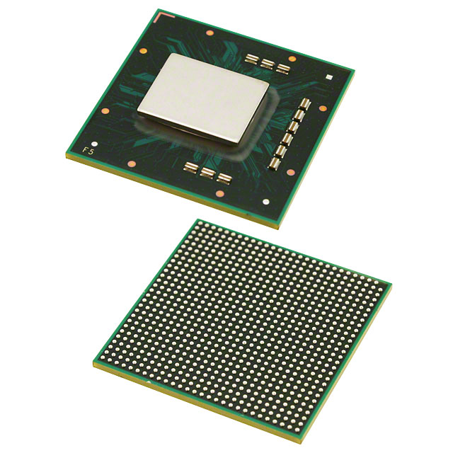
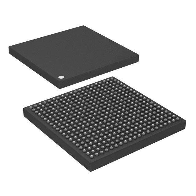
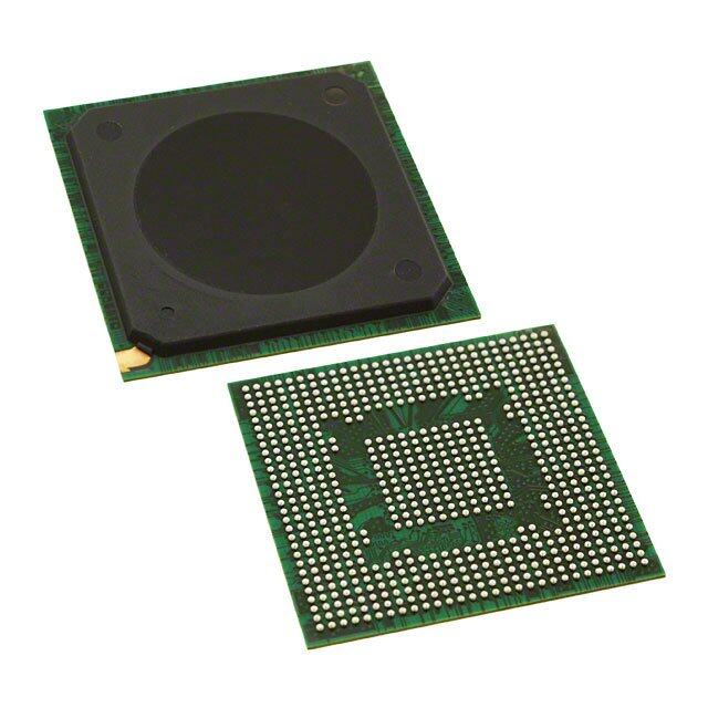
| 描述 | IC MPU POWERQUICC III 783-FCPBGA |
| Display&InterfaceControllers | - |
| 产品分类 | |
| GraphicsAcceleration | - |
| 品牌 | Freescale Semiconductor |
| NumberofCores/BusWidth | * |
| 数据手册 | |
| 产品图片 |
|
| 产品型号 | MPC8555ECPXALF |
| PCN设计/规格 | http://cache.freescale.com/files/shared/doc/pcn/PCN16462.htm |
| RAMControllers | * |
| RAM控制器 | DDR, SDRAM |
| rohs | 含铅 / 不符合限制有害物质指令(RoHS)规范要求 |
| SATA | - |
| SecurityFeatures | * |
| 产品系列 | MPC85xx |
| USB | USB 2.0(1) |
| 以太网 | 10/100/1000 Mbps (2) |
| 供应商器件封装 | 783-FCPBGA(29x29) |
| 包装 | 托盘 |
| 协处理器/DSP | 通信; CPM, 安全; SEC |
| 图形加速 | 无 |
| 处理器类型 | 32-位 MPC85xx PowerQUICC III |
| 安全特性 | 密码技术,随机数发生器 |
| 安装类型 | 表面贴装 |
| 封装/外壳 | 783-BBGA,FCBGA |
| 工作温度 | -40°C ~ 105°C |
| 显示与接口控制器 | - |
| 标准包装 | 180 |
| 核心处理器 | PowerPC e500 |
| 核数/总线宽度 | 1 코어, 32 位 |
| 特性 | - |
| 电压 | 1.2V |
| 电压-I/O | 2.5V, 3.3V |
| 速度 | 667MHz |
| 配用 | /product-detail/zh/CWH-PPC-8540N-VE/CWH-PPC-8540N-VE-ND/1790894 |
| 附加接口 | DUART, I²C, PCI, SPI, TDM, UART |


- 商务部:美国ITC正式对集成电路等产品启动337调查
- 曝三星4nm工艺存在良率问题 高通将骁龙8 Gen1或转产台积电
- 太阳诱电将投资9.5亿元在常州建新厂生产MLCC 预计2023年完工
- 英特尔发布欧洲新工厂建设计划 深化IDM 2.0 战略
- 台积电先进制程称霸业界 有大客户加持明年业绩稳了
- 达到5530亿美元!SIA预计今年全球半导体销售额将创下新高
- 英特尔拟将自动驾驶子公司Mobileye上市 估值或超500亿美元
- 三星加码芯片和SET,合并消费电子和移动部门,撤换高东真等 CEO
- 三星电子宣布重大人事变动 还合并消费电子和移动部门
- 海关总署:前11个月进口集成电路产品价值2.52万亿元 增长14.8%
PDF Datasheet 数据手册内容提取
Freescale Semiconductor MPC8555EEC Rev. 4.2, 1/2008 Technical Data MPC8555E PowerQUICC™ III Integrated Communications Processor Hardware Specification The MPC8555E integrates a PowerPC™ processor core Contents built on Power Architecture™ technology with system logic 1. Overview . . . . . . . . . . . . . . . . . . . . . . . . . . . . . . . . . . . . 2 2. Electrical Characteristics . . . . . . . . . . . . . . . . . . . . . . . . 8 required for networking, telecommunications, and wireless 3. Power Characteristics . . . . . . . . . . . . . . . . . . . . . . . . . 13 infrastructure applications. The MPC8555E is a member of 4. Clock Timing . . . . . . . . . . . . . . . . . . . . . . . . . . . . . . . . 15 the PowerQUICC™ III family of devices that combine 5. RESET Initialization . . . . . . . . . . . . . . . . . . . . . . . . . . 16 6. DDR SDRAM . . . . . . . . . . . . . . . . . . . . . . . . . . . . . . . 17 system-level support for industry-standard interfaces with 7. DUART . . . . . . . . . . . . . . . . . . . . . . . . . . . . . . . . . . . . 21 processors that implement the embedded category of the 8. Ethernet: Three-Speed, MII Management . . . . . . . . . . 22 Power Architecture technology. For functional 9. Local Bus . . . . . . . . . . . . . . . . . . . . . . . . . . . . . . . . . . . 33 characteristics of the processor, refer to the MPC8555E 10. CPM . . . . . . . . . . . . . . . . . . . . . . . . . . . . . . . . . . . . . . . 43 11. JTAG . . . . . . . . . . . . . . . . . . . . . . . . . . . . . . . . . . . . . . 50 PowerQUICC™ III Integrated Communications Processor 12. I2C . . . . . . . . . . . . . . . . . . . . . . . . . . . . . . . . . . . . . . . . 52 Reference Manual. 13. PCI . . . . . . . . . . . . . . . . . . . . . . . . . . . . . . . . . . . . . . . . 54 14. Package and Pin Listings . . . . . . . . . . . . . . . . . . . . . . . 56 To locate any published errata or updates for this document 15. Clocking . . . . . . . . . . . . . . . . . . . . . . . . . . . . . . . . . . . . 66 refer to http://www.freescale.com or contact your Freescale 16. Thermal . . . . . . . . . . . . . . . . . . . . . . . . . . . . . . . . . . . . 69 sales office. 17. System Design Information . . . . . . . . . . . . . . . . . . . . . 78 18. Document Revision History . . . . . . . . . . . . . . . . . . . . 85 19. Device Nomenclature . . . . . . . . . . . . . . . . . . . . . . . . . 86 ©Freescale Semiconductor, Inc., 2008. All rights reserved.
Overview 1 Overview The following section provides a high-level overview of the MPC8555E features. Figure 1 shows the major functional units within the MPC8555E. DDR DDR SDRAM Controller SDRAM Security 256-Kbyte Engine L2 Cache/ I2C Controller SRAM e500 Core DUART e500 32-Kbyte L1 32-Kbyte L1 Coherency I Cache D Cache Module Core Complex GPIO Local Bus Controller Bus 32b Programmable IRQs Interrupt Controller Serial CPM DMA 64/32b PCI Controller MPHY FCC OCeaN UTOPIA ner FCC ROM 0/32b PCI Controller g ssi SCC A I-Memory MIIs/RMIIs ot SCC/USB DMA Controller s Sl ace me- SCC DPRAM TDMs erf Ti SMC al Int SMC ERnIgSiCne 10/100/1000 MAC eri SPI MII, GMII, TBI, I/Os S I2C Parallel I/O RTBI, RGMIIs 10/100/1000 MAC Baud Rate Generators Timers CPM Interrupt Controller Figure1. MPC8555E Block Diagram 1.1 Key Features The following lists an overview of the MPC8555E feature set. (cid:129) Embedded e500 Book E-compatible core — High-performance, 32-bit Book E-enhanced core that implements the PowerPC architecture — Dual-issue superscalar, 7-stage pipeline design — 32-Kbyte L1 instruction cache and 32-Kbyte L1 data cache with parity protection — Lockable L1 caches—entire cache or on a per-line basis — Separate locking for instructions and data — Single-precision floating-point operations — Memory management unit especially designed for embedded applications — Enhanced hardware and software debug support — Dynamic power management — Performance monitor facility MPC8555E PowerQUICC™ III Integrated Communications Processor Hardware Specification, Rev. 4.2 2 Freescale Semiconductor
Overview (cid:129) Security Engine is optimized to handle all the algorithms associated with IPSec, SSL/TLS, SRTP, IEEE Std 802.11i™, iSCSI, and IKE processing. The Security Engine contains 4 Crypto-channels, a Controller, and a set of crypto Execution Units (EUs). The Execution Units are: — Public Key Execution Unit (PKEU) supporting the following: – RSA and Diffie-Hellman – Programmable field size up to 2048-bits – Elliptic curve cryptography – F2m and F(p) modes – Programmable field size up to 511-bits — Data Encryption Standard Execution Unit (DEU) – DES, 3DES – Two key (K1, K2) or Three Key (K1, K2, K3) – ECB and CBC modes for both DES and 3DES — Advanced Encryption Standard Unit (AESU) – Implements the Rinjdael symmetric key cipher – Key lengths of 128, 192, and 256 bits.Two key – ECB, CBC, CCM, and Counter modes — ARC Four execution unit (AFEU) – Implements a stream cipher compatible with the RC4 algorithm – 40- to 128-bit programmable key — Message Digest Execution Unit (MDEU) – SHA with 160-bit or 256-bit message digest – MD5 with 128-bit message digest – HMAC with either algorithm — Random Number Generator (RNG) — 4 Crypto-channels, each supporting multi-command descriptor chains – Static and/or dynamic assignment of crypto-execution units via an integrated controller – Buffer size of 256 Bytes for each execution unit, with flow control for large data sizes (cid:129) High-performance RISC CPM operating at up to 333 MHz — CPM software compatibility with previous PowerQUICC families — One instruction per clock — Executes code from internal ROM or instruction RAM — 32-bit RISC architecture — Tuned for communication environments: instruction set supports CRC computation and bit manipulation. — Internal timer — Interfaces with the embedded e500 core processor through a 32-Kbyte dual-port RAM and virtual DMA channels for each peripheral controller — Handles serial protocols and virtual DMA MPC8555E PowerQUICC™ III Integrated Communications Processor Hardware Specification, Rev. 4.2 Freescale Semiconductor 3
Overview — Two full-duplex fast communications controllers (FCCs) that support the following protocols: – ATM protocol through two UTOPIA level 2 interfaces – IEEE Std 802.3™/Fast Ethernet (10/100) – HDLC – Totally transparent operation — Three full-duplex serial communications controllers (SCCs) support the following protocols: – High level/synchronous data link control (HDLC/SDLC) – LocalTalk (HDLC-based local area network protocol) – Universal asynchronous receiver transmitter (UART) – Synchronous UART (1x clock mode) – Binary synchronous communication (BISYNC) – Totally transparent operation – QMC support, providing 64 channels per SCC using only one physical TDM interface — Universal serial bus (USB) controller that is full/low-speed compliant (multiplexed on an SCC) – USB host mode – Supports USB slave mode — Serial peripheral interface (SPI) support for master or slave — I2C bus controller — Two serial management controllers (SMCs) supporting: – UART – Transparent – General-circuit interfaces (GCI) — Time-slot assigner supports multiplexing of data from any of the SCCs and FCCs onto eight time-division multiplexed (TDM) interfaces. The time-slot assigner supports the following TDM formats: – T1/CEPT lines – T3/E3 – Pulse code modulation (PCM) highway interface – ISDN primary rate – Freescale interchip digital link (IDL) – General circuit interface (GCI) — User-defined interfaces — Eight independent baud rate generators (BRGs) — Four general-purpose 16-bit timers or two 32-bit timers — General-purpose parallel ports—16 parallel I/O lines with interrupt capability (cid:129) 256 Kbytes of on-chip memory — Can act as a 256-Kbyte level-2 cache — Can act as a 256-Kbyte or two 128-Kbyte memory-mapped SRAM arrays MPC8555E PowerQUICC™ III Integrated Communications Processor Hardware Specification, Rev. 4.2 4 Freescale Semiconductor
Overview — Can be partitioned into 128-Kbyte L2 cache plus 128-Kbyte SRAM — Full ECC support on 64-bit boundary in both cache and SRAM modes — SRAM operation supports relocation and is byte-accessible — Cache mode supports instruction caching, data caching, or both — External masters can force data to be allocated into the cache through programmed memory ranges or special transaction types (stashing). — Eight-way set-associative cache organization (1024 sets of 32-byte cache lines) — Supports locking the entire cache or selected lines – Individual line locks set and cleared through Book E instructions or by externally mastered transactions — Global locking and flash clearing done through writes to L2 configuration registers — Instruction and data locks can be flash cleared separately — Read and write buffering for internal bus accesses (cid:129) Address translation and mapping unit (ATMU) — Eight local access windows define mapping within local 32-bit address space — Inbound and outbound ATMUs map to larger external address spaces – Three inbound windows plus a configuration window on PCI – Four inbound windows – Four outbound windows plus default translation for PCI (cid:129) DDR memory controller — Programmable timing supporting first generation DDR SDRAM — 64-bit data interface, up to MHz data rate — Four banks of memory supported, each up to 1 Gbyte — DRAM chip configurations from 64 Mbits to 1 Gbit with x8/x16 data ports — Full ECC support — Page mode support (up to 16 simultaneous open pages) — Contiguous or discontiguous memory mapping — Sleep mode support for self refresh DDR SDRAM — Supports auto refreshing — On-the-fly power management using CKE signal — Registered DIMM support — Fast memory access via JTAG port — 2.5-V SSTL2 compatible I/O (cid:129) Programmable interrupt controller (PIC) — Programming model is compliant with the OpenPIC architecture — Supports 16 programmable interrupt and processor task priority levels — Supports 12 discrete external interrupts — Supports 4 message interrupts with 32-bit messages MPC8555E PowerQUICC™ III Integrated Communications Processor Hardware Specification, Rev. 4.2 Freescale Semiconductor 5
Overview — Supports connection of an external interrupt controller such as the 8259 programmable interrupt controller — Four global high resolution timers/counters that can generate interrupts — Supports additional internal interrupt sources — Supports fully nested interrupt delivery — Interrupts can be routed to external pin for external processing — Interrupts can be routed to the e500 core’s standard or critical interrupt inputs — Interrupt summary registers allow fast identification of interrupt source (cid:129) Two I 2C controllers (one is contained within the CPM, the other is a stand-alone controller which is not part of the CPM) — Two-wire interface — Multiple master support — Master or slave I2C mode support — On-chip digital filtering rejects spikes on the bus (cid:129) Boot sequencer — Optionally loads configuration data from serial ROM at reset via the stand-alone I2C interface — Can be used to initialize configuration registers and/or memory — Supports extended I2C addressing mode — Data integrity checked with preamble signature and CRC (cid:129) DUART — Two 4-wire interfaces (RXD, TXD, RTS, CTS) — Programming model compatible with the original 16450 UART and the PC16550D (cid:129) Local bus controller (LBC) — Multiplexed 32-bit address and data operating at up to 166 MHz — Eight chip selects support eight external slaves — Up to eight-beat burst transfers — The 32-, 16-, and 8-bit port sizes are controlled by an on-chip memory controller — Three protocol engines available on a per chip select basis: – General purpose chip select machine (GPCM) – Three user programmable machines (UPMs) – Dedicated single data rate SDRAM controller — Parity support — Default boot ROM chip select with configurable bus width (8-, 16-, or 32-bit) (cid:129) Two Three-speed (10/100/1000)Ethernet controllers (TSECs) — Dual IEEE 802.3, 802.3u, 802.3x, 802.3z AC compliant controllers — Support for Ethernet physical interfaces: – 10/100/1000 Mbps IEEE 802.3 GMII – 10/100 Mbps IEEE 802.3 MII MPC8555E PowerQUICC™ III Integrated Communications Processor Hardware Specification, Rev. 4.2 6 Freescale Semiconductor
Overview – 10 Mbps IEEE 802.3 MII – 1000 Mbps IEEE 802.3z TBI – 10/100/1000 Mbps RGMII/RTBI — Full- and half-duplex support — Buffer descriptors are backwards compatible with MPC8260 and MPC860T 10/100 programming models — 9.6-Kbyte jumbo frame support — RMON statistics support — 2-Kbyte internal transmit and receive FIFOs — MII management interface for control and status — Programmable CRC generation and checking (cid:129) OCeaN switch fabric — Three-port crossbar packet switch — Reorders packets from a source based on priorities — Reorders packets to bypass blocked packets — Implements starvation avoidance algorithms — Supports packets with payloads of up to 256 bytes (cid:129) Integrated DMA controller — Four-channel controller — All channels accessible by both local and remote masters — Extended DMA functions (advanced chaining and striding capability) — Support for scatter and gather transfers — Misaligned transfer capability — Interrupt on completed segment, link, list, and error — Supports transfers to or from any local memory or I/O port — Selectable hardware-enforced coherency (snoop/no-snoop) — Ability to start and flow control each DMA channel from external 3-pin interface — Ability to launch DMA from single write transaction (cid:129) PCI Controllers — PCI 2.2 compatible — One 64-bit or two 32-bit PCI ports supported at 16 to 66 MHz — Host and agent mode support, 64-bit PCI port can be host or agent, if two 32-bit ports, only one can be an agent — 64-bit dual address cycle (DAC) support — Supports PCI-to-memory and memory-to-PCI streaming — Memory prefetching of PCI read accesses — Supports posting of processor-to-PCI and PCI-to-memory writes MPC8555E PowerQUICC™ III Integrated Communications Processor Hardware Specification, Rev. 4.2 Freescale Semiconductor 7
Electrical Characteristics — PCI 3.3-V compatible — Selectable hardware-enforced coherency — Selectable clock source (SYSCLK or independent PCI_CLK) (cid:129) Power management — Fully static 1.2-V CMOS design with 3.3- and 2.5-V I/O — Supports power save modes: doze, nap, and sleep — Employs dynamic power management — Selectable clock source (sysclk or independent PCI_CLK) (cid:129) System performance monitor — Supports eight 32-bit counters that count the occurrence of selected events — Ability to count up to 512 counter specific events — Supports 64 reference events that can be counted on any of the 8 counters — Supports duration and quantity threshold counting — Burstiness feature that permits counting of burst events with a programmable time between bursts — Triggering and chaining capability — Ability to generate an interrupt on overflow (cid:129) System access port — Uses JTAG interface and a TAP controller to access entire system memory map — Supports 32-bit accesses to configuration registers — Supports cache-line burst accesses to main memory — Supports large block (4-Kbyte) uploads and downloads — Supports continuous bit streaming of entire block for fast upload and download (cid:129) IEEE Std 1149.1™-compatible, JTAG boundary scan (cid:129) 783 FC-PBGA package 2 Electrical Characteristics This section provides the AC and DC electrical specifications and thermal characteristics for the MPC8555E. The MPC8555E is currently targeted to these specifications. Some of these specifications are independent of the I/O cell, but are included for a more complete reference. These are not purely I/O buffer design specifications. 2.1 Overall DC Electrical Characteristics This section covers the ratings, conditions, and other characteristics. MPC8555E PowerQUICC™ III Integrated Communications Processor Hardware Specification, Rev. 4.2 8 Freescale Semiconductor
Electrical Characteristics 2.1.1 Absolute Maximum Ratings Table 1 provides the absolute maximum ratings. Table1. Absolute Maximum Ratings 1 Characteristic Symbol Max Value Unit Notes Core supply voltage V –0.3 to 1.32 V DD 0.3 to 1.43 (for 1 GHz only) PLL supply voltage AV –0.3 to 1.32 V DD 0.3 to 1.43 (for 1 GHz only) DDR DRAM I/O voltage GV –0.3 to 3.63 V DD Three-speed Ethernet I/O, MII management voltage LV –0.3 to 3.63 V DD –0.3 to 2.75 CPM, PCI, local bus, DUART, system control and power OV –0.3 to 3.63 V 3 DD management, I2C, and JTAG I/O voltage Input voltage DDR DRAM signals MV –0.3 to (GV + 0.3) V 2, 5 IN DD DDR DRAM reference MV –0.3 to (GV + 0.3) V 2, 5 REF DD Three-speed Ethernet signals LV –0.3 to (LV + 0.3) V 4, 5 IN DD CPM, Local bus, DUART, OV –0.3 to (OV + 0.3)1 V 5 IN DD SYSCLK, system control and power management, I2C, and JTAG signals PCI OV –0.3 to (OV + 0.3) V 6 IN DD Storage temperature range T –55 to 150 °C STG Notes: 1. Functional and tested operating conditions are given in Table2. Absolute maximum ratings are stress ratings only, and functional operation at the maximums is not guaranteed. Stresses beyond those listed may affect device reliability or cause permanent damage to the device. 2. Caution: MV must not exceed GV by more than 0.3 V. This limit may be exceeded for a maximum of 20 ms during IN DD power-on reset and power-down sequences. 3. Caution: OV must not exceed OV by more than 0.3 V. This limit may be exceeded for a maximum of 20 ms during IN DD power-on reset and power-down sequences. 4. Caution: LV must not exceed LV by more than 0.3 V. This limit may be exceeded for a maximum of 20 ms during IN DD power-on reset and power-down sequences. 5. (M,L,O)V and MV may overshoot/undershoot to a voltage and for a maximum duration as shown in Figure2. IN REF 6. OV on the PCI interface may overshoot/undershoot according to the PCI Electrical Specification for 3.3-V operation, as IN shown in Figure3. 2.1.2 Power Sequencing The MPC8555Erequires its power rails to be applied in a specific sequence in order to ensure proper device operation. These requirements are as follows for power up: 1. V , AV DD DDn 2. GV , LV , OV (I/O supplies) DD DD DD MPC8555E PowerQUICC™ III Integrated Communications Processor Hardware Specification, Rev. 4.2 Freescale Semiconductor 9
Electrical Characteristics Items on the same line have no ordering requirement with respect to one another. Items on separate lines must be ordered sequentially such that voltage rails on a previous step must reach 90 percent of their value before the voltage rails on the current step reach ten percent of theirs. NOTE If the items on line 2 must precede items on line 1, please ensure that the delay does not exceed 500 ms and the power sequence is not done greater than once per day in production environment. NOTE From a system standpoint, if the I/O power supplies ramp prior to the V DD core supply, the I/Os on the MPC8555E may drive a logic one or zero during power-up. 2.1.3 Recommended Operating Conditions Table 2 provides the recommended operating conditions for the MPC8555E. Note that the values in Table 2 are the recommended and tested operating conditions. Proper device operation outside of these conditions is not guaranteed. Table2. Recommended Operating Conditions Characteristic Symbol Recommended Value Unit Core supply voltage V 1.2 V ± 60 mV V DD 1.3 V± 50 mV (for 1 GHz only) PLL supply voltage AV 1.2 V ± 60 mV V DD 1.3 V ± 50 mV (for 1 GHz only) DDR DRAM I/O voltage GV 2.5 V ± 125 mV V DD Three-speed Ethernet I/O voltage LV 3.3 V ± 165 mV V DD 2.5 V ± 125 mV PCI, local bus, DUART, system control and power management, OV 3.3 V ± 165 mV V DD I2C, and JTAG I/O voltage Input voltage DDR DRAM signals MV GND to GV V IN DD DDR DRAM reference MV GND to GV V REF DD Three-speed Ethernet signals LV GND to LV V IN DD PCI, local bus, DUART, OV GND to OV V IN DD SYSCLK, system control and power management, I2C, and JTAG signals Die-junction Temperature T 0 to 105 °C j MPC8555E PowerQUICC™ III Integrated Communications Processor Hardware Specification, Rev. 4.2 10 Freescale Semiconductor
Electrical Characteristics Figure 2 shows the undershoot and overshoot voltages at the interfaces of the MPC8555E. G/L/OV + 20% DD G/L/OV + 5% DD VIH G/L/OVDD GND GND – 0.3 V V IL GND – 0.7 V Not to Exceed 10% of t 1 Note: SYS 1. Note that t refers to the clock period associated with the SYSCLK signal. SYS Figure2. Overshoot/Undershoot Voltage for GV /OV /LV DD DD DD The MPC8555E core voltage must always be provided at nominal 1.2 V (see Table 2 for actual recommended core voltage). Voltage to the processor interface I/Os are provided through separate sets of supply pins and must be provided at the voltages shown in Table 2. The input voltage threshold scales with respect to the associated I/O supply voltage. OV and LV based receivers are simple CMOS I/O DD DD circuits and satisfy appropriate LVCMOS type specifications. The DDR SDRAM interface uses a single-ended differential receiver referenced the externally supplied MV signal (nominally set to REF GV /2) as is appropriate for the SSTL2 electrical signaling standard. DD MPC8555E PowerQUICC™ III Integrated Communications Processor Hardware Specification, Rev. 4.2 Freescale Semiconductor 11
Electrical Characteristics Figure 3 shows the undershoot and overshoot voltage of the PCI interface of the MPC8555E for the 3.3-V signals, respectively. 11 ns (Min) +7.1 V Overvoltage 7.1 V p-to-p Waveform (Min) 0 V 4 ns (Max) 4 ns (Max) 62.5 ns +3.6 V Undervoltage 7.1 V p-to-p Waveform (Min) –3.5 V Figure3. Maximum AC Waveforms on PCI interface for 3.3-V Signaling 2.1.4 Output Driver Characteristics Table 3 provides information on the characteristics of the output driver strengths. The values are preliminary estimates. Table3. Output Drive Capability Programmable Output Supply Driver Type Notes Impedance (Ω) Voltage Local bus interface utilities signals 25 OV = 3.3 V 1 DD 42 (default) PCI signals 25 2 42 (default) DDR signal 20 GV = 2.5 V DD TSEC/10/100 signals 42 LV = 2.5/3.3 V DD DUART, system control, I2C, JTAG 42 OV = 3.3 V DD Notes: 1. The drive strength of the local bus interface is determined by the configuration of the appropriate bits in PORIMPSCR. 2. The drive strength of the PCI interface is determined by the setting of the PCI_GNT1 signal at reset. MPC8555E PowerQUICC™ III Integrated Communications Processor Hardware Specification, Rev. 4.2 12 Freescale Semiconductor
Power Characteristics 3 Power Characteristics The estimated typical power dissipation for this family of PowerQUICC III devices is shown in Table 4. Table4. Power Dissipation(1) (2) CCB Frequency (MHz) Core Frequency (MHz) V Typical Power(3)(4) (W) Maximum Power(5) (W) DD 200 400 1.2 4.9 6.6 500 1.2 5.2 7.0 600 1.2 5.5 7.3 267 533 1.2 5.4 7.2 667 1.2 5.9 7.7 800 1.2 6.3 9.1 333 667 1.2 6.0 7.9 833 1.2 6.5 9.3 1000(6) 1.3 9.6 12.8 Notes: 1. The values do not include I/O supply power (OV , LV , GV ) or AV DD DD DD DD. 2. Junction temperature is a function of die size, on-chip power dissipation, package thermal resistance, mounting site (board) temperature, ambient temperature, air flow, power dissipation of other components on the board, and board thermal resistance. Any customer design must take these considerations into account to ensure the maximum 105 degrees junction temperature is not exceeded on this device. 3. Typical power is based on a nominal voltage of V = 1.2V, a nominal process, a junction temperature of T = 105° C, and a DD j Dhrystone 2.1 benchmark application. 4. Thermal solutions likely need to design to a value higher than Typical Power based on the end application, T target, and I/O A power 5. Maximum power is based on a nominal voltage of V = 1.2V, worst case process, a junction temperature of T = 105° C, and DD j an artificial smoke test. 6. The nominal recommended V = 1.3V for this speed grade. DD Notes: 1. 2. 3. 4. 5. 6. MPC8555E PowerQUICC™ III Integrated Communications Processor Hardware Specification, Rev. 4.2 Freescale Semiconductor 13
Power Characteristics Table5. Typical I/O Power Dissipation GV OV LV LV Interface Parameters DD DD DD DD Unit Comments (2.5 V) (3.3 V) (3.3 V) (2.5 V) DDR I/O CCB = 200 MHz 0.46 — — — W — CCB = 266 MHz 0.59 — — — W — CCB = 300 MHz 0.66 — — — W — CCB = 333 MHz 0.73 — — — W — PCI I/O 64b, 66 MHz — 0.14 — — W — 64b, 33 MHz — 0.08 — — W — 32b, 66 MHz — 0.07 — — W Multiply by 2 if using two 32b ports 32b, 33 MHz — 0.04 — — W Local Bus I/O 32b, 167 MHz — 0.30 — — W — 32b, 133 MHz — 0.24 — — W — 32b, 83 MHz — 0.16 — — W — 32b, 66 MHz — 0.13 — — W — 32b, 33 MHz — 0.07 — — W — TSEC I/O MII — — 0.01 — W Multiply by number of interfaces used. GMII or TBI — — 0.07 — W RGMII or RTBI — — — 0.04 W CPM - FCC MII — 0.015 — — W — RMII — 0.013 — — W — HDLC 16 Mbps — 0.009 — — W — UTOPIA-8 SPHY — 0.06 — — W — UTOPIA-8 MPHY — 0.1 — — W — UTOPIA-16 SPHY — 0.094 — — W — UTOPIA-16 MPHY — 0.135 — — W — CPM - SCC HDLC 16 Mbps — 0.004 — — W — TDMA or TDMB Nibble Mode — 0.01 — — W — TDMA or TDMB Per Channel — 0.005 — — W Up to 4 TDM channels, multiply by number of TDM channels. MPC8555E PowerQUICC™ III Integrated Communications Processor Hardware Specification, Rev. 4.2 14 Freescale Semiconductor
Clock Timing 4 Clock Timing 4.1 System Clock Timing Table 6 provides the system clock (SYSCLK) AC timing specifications for the MPC8555E. Table6. SYSCLK AC Timing Specifications Parameter/Condition Symbol Min Typical Max Unit Notes SYSCLK frequency f — — 166 MHz 1 SYSCLK SYSCLK cycle time t 6.0 — — ns — SYSCLK SYSCLK rise and fall time t , t 0.6 1.0 1.2 ns 2 KH KL SYSCLK duty cycle t /t 40 — 60 % 3 KHK SYSCLK SYSCLK jitter — — — +/- 150 ps 4, 5 Notes: 1.Caution: The CCB to SYSCLK ratio and e500 core to CCB ratio settings must be chosen such that the resulting SYSCLK frequency, e500 (core) frequency, and CCB frequency do not exceed their respective maximum or minimum operating frequencies. 2. Rise and fall times for SYSCLK are measured at 0.6 and 2.7 V. 3. Timing is guaranteed by design and characterization. 4. This represents the total input jitter—short term and long term—and is guaranteed by design. 5. For spread spectrum clocking, guidelines are ±1% of the input frequency with a maximum of 60 kHz of modulation regardless of the input frequency. 4.2 TSEC Gigabit Reference Clock Timing Table 7 provides the TSEC gigabit reference clock (EC_GTX_CLK125) AC timing specifications for the MPC8555E. Table7. EC_GTX_CLK125 AC Timing Specifications Parameter/Condition Symbol Min Typical Max Unit Notes EC_GTX_CLK125 frequency f — 125 — MHz — G125 EC_GTX_CLK125 cycle time t — 8 — ns — G125 EC_GTX_CLK125 rise time t — — 1.0 ns 1 G125R EC_GTX_CLK125 fall time t — — 1.0 ns 1 G125F EC_GTX_CLK125 duty cycle t /t — % 1, 2 G125H G125 GMII, TBI 45 55 RGMII, RTBI 47 53 Notes: 1. Timing is guaranteed by design and characterization. 2. EC_GTX_CLK125 is used to generate GTX clock for TSEC transmitter with 2% degradation. EC_GTX_CLK125 duty cycle can be loosened from 47/53% as long as PHY device can tolerate the duty cycle generated by GTX_CLK of TSEC. MPC8555E PowerQUICC™ III Integrated Communications Processor Hardware Specification, Rev. 4.2 Freescale Semiconductor 15
RESET Initialization 4.3 Real Time Clock Timing Table 8 provides the real time clock (RTC) AC timing specifications. Table8. RTC AC Timing Specifications Parameter/Condition Symbol Min Typical Max Unit Notes RTC clock high time t 2 x — — ns — RTCH t CCB_CLK RTC clock low time t 2 x — — ns — RTCL t CCB_CLK 5 RESET Initialization This section describes the AC electrical specifications for the RESET initialization timing requirements of the MPC8555E. Table 9 provides the RESET initialization AC timing specifications. Table9. RESET Initialization Timing Specifications Parameter/Condition Min Max Unit Notes Required assertion time of HRESET 100 — μs — Minimum assertion time for SRESET 512 — SYSCLKs 1 PLL input setup time with stable SYSCLK before HRESET 100 — μs — negation Input setup time for POR configs (other than PLL config) with 4 — SYSCLKs 1 respect to negation of HRESET Input hold time for POR configs (including PLL config) with 2 — SYSCLKs 1 respect to negation of HRESET Maximum valid-to-high impedance time for actively driven POR — 5 SYSCLKs 1 configs with respect to negation of HRESET Notes: 1.SYSCLK is identical to the PCI_CLK signal and is the primary clock input for the MPC8555E. See the MPC8555E PowerQUICC™ III Integrated Communications Processor Reference Manual for more details. Table 10 provides the PLL and DLL lock times. Table10. PLL and DLL Lock Times Parameter/Condition Min Max Unit Notes PLL lock times — 100 μs — DLL lock times 7680 122,880 CCB Clocks 1, 2 Notes: 1.DLL lock times are a function of the ratio between the output clock and the platform (or CCB) clock. A 2:1 ratio results in the minimum and an 8:1 ratio results in the maximum. 2. The CCB clock is determined by the SYSCLK × platform PLL ratio. MPC8555E PowerQUICC™ III Integrated Communications Processor Hardware Specification, Rev. 4.2 16 Freescale Semiconductor
DDR SDRAM 6 DDR SDRAM This section describes the DC and AC electrical specifications for the DDR SDRAM interface of the MPC8555E. 6.1 DDR SDRAM DC Electrical Characteristics Table 11 provides the recommended operating conditions for the DDR SDRAM component(s) of the MPC8555E. Table11. DDR SDRAM DC Electrical Characteristics Parameter/Condition Symbol Min Max Unit Notes I/O supply voltage GV 2.375 2.625 V 1 DD I/O reference voltage MV 0.49 × GV 0.51 × GV V 2 REF DD DD I/O termination voltage V MV – 0.04 MV + 0.04 V 3 TT REF REF Input high voltage V MV + 0.18 GV + 0.3 V — IH REF DD Input low voltage V –0.3 MV – 0.18 V — IL REF Output leakage current I –10 10 μA 4 OZ Output high current (V = 1.95 V) I –15.2 — mA — OUT OH Output low current (V = 0.35 V) I 15.2 — mA — OUT OL MV input leakage current I — 5 μA — REF VREF Notes: 1.GV is expected to be within 50 mV of the DRAM GV at all times. DD DD 2.MV is expected to be equal to 0.5 × GV , and to track GV DC variations as measured at the receiver. Peak-to-peak REF DD DD noise on MV may not exceed ±2% of the DC value. REF 3.V is not applied directly to the device. It is the supply to which far end signal termination is made and is expected to be TT equal to MV . This rail should track variations in the DC level of MV . REF REF 4.Output leakage is measured with all outputs disabled, 0 V ≤ V ≤ GV . OUT DD Table 12 provides the DDR capacitance. Table12. DDR SDRAM Capacitance Parameter/Condition Symbol Min Max Unit Notes Input/output capacitance: DQ, DQS, MSYNC_IN C 6 8 pF 1 IO Delta input/output capacitance: DQ, DQS C — 0.5 pF 1 DIO Note: 1.This parameter is sampled. GV = 2.5 V ± 0.125 V, f = 1 MHz, T = 25°C, V = GV /2, V (peak to peak)= 0.2V. DD A OUT DD OUT MPC8555E PowerQUICC™ III Integrated Communications Processor Hardware Specification, Rev. 4.2 Freescale Semiconductor 17
DDR SDRAM 6.2 DDR SDRAM AC Electrical Characteristics This section provides the AC electrical characteristics for the DDR SDRAM interface. 6.2.1 DDR SDRAM Input AC Timing Specifications Table 13 provides the input AC timing specifications for the DDR SDRAM interface. Table13. DDR SDRAM Input AC Timing Specifications At recommended operating conditions with GV of 2.5 V ± 5%. DD Parameter Symbol Min Max Unit Notes AC input low voltage V — MV – 0.31 V — IL REF AC input high voltage V MV + 0.31 GV + 0.3 V — IH REF DD MDQS—MDQ/MECC input skew per t — ps 1 DISKEW byte For DDR = 333 MHz 750 For DDR < 266 MHz 1125 Note: 1.Maximum possible skew between a data strobe (MDQS[n]) and any corresponding bit of data (MDQ[8n+{0...7}] if 0 <= n <= 7) or ECC (MECC[{0...7}] if n = 8). 6.2.2 DDR SDRAM Output AC Timing Specifications Table 14 and Table15 provide the output AC timing specifications and measurement conditions for the DDR SDRAM interface. Table14. DDR SDRAM Output AC Timing Specifications for Source Synchronous Mode At recommended operating conditions with GV of 2.5 V ± 5%. DD Parameter Symbol 1 Min Max Unit Notes MCK[n] cycle time, (MCK[n]/MCK[n] crossing) t 6 10 ns 2 MCK Skew between any MCK to ADDR/CMD t ps 3 AOSKEW 333 MHz –1000 200 266 MHz –1100 300 200 MHz –1200 400 ADDR/CMD output setup with respect to MCK t — ns 4 DDKHAS 333 MHz 2.8 266 MHz 3.45 200 MHz 4.6 ADDR/CMD output hold with respect to MCK t — ns 4 DDKHAX 333 MHz 2.0 266 MHz 2.65 200 MHz 3.8 MCS(n) output setup with respect to MCK t — ns 4 DDKHCS 333 MHz 2.8 266 MHz 3.45 200 MHz 4.6 MPC8555E PowerQUICC™ III Integrated Communications Processor Hardware Specification, Rev. 4.2 18 Freescale Semiconductor
DDR SDRAM Table14. DDR SDRAM Output AC Timing Specifications for Source Synchronous Mode (continued) At recommended operating conditions with GV of 2.5 V ± 5%. DD Parameter Symbol 1 Min Max Unit Notes MCS(n) output hold with respect to MCK t — ns 4 DDKHCX 333 MHz 2.0 266 MHz 2.65 200 MHz 3.8 MCK to MDQS t ns 5 DDKHMH 333 MHz –0.9 0.3 266 MHz –1.1 0.5 200 MHz –1.2 0.6 MDQ/MECC/MDM output setup with respect to t — ps 6 DDKHDS, MDQS t DDKLDS 333 MHz 900 266 MHz 900 200 MHz 1200 MDQ/MECC/MDM output hold with respect to t — ps 6 DDKHDX, MDQS t DDKLDX 333 MHz 900 266 MHz 900 200 MHz 1200 MDQS preamble start t –0.5 × t – 0.9 –0.5 × t +0.3 ns 7 DDKHMP MCK MCK MDQS epilogue end t –0.9 0.3 ns 7 DDKLME Notes: 1. The symbols used for timing specifications follow the pattern of t for (first two letters of functional block)(signal)(state) (reference)(state) inputs and t for outputs. Output hold time can be read as DDR timing (first two letters of functional block)(reference)(state)(signal)(state) (DD) from the rising or falling edge of the reference clock (KH or KL) until the output went invalid (AX or DX). For example, t symbolizes DDR timing (DD) for the time t memory clock reference (K) goes from the high (H) state until DDKHAS MCK outputs (A) are setup (S) or output valid time. Also, t symbolizes DDR timing (DD) for the time t memory clock DDKLDX MCK reference (K) goes low (L) until data outputs (D) are invalid (X) or data output hold time. 2. All MCK/MCK referenced measurements are made from the crossing of the two signals ±0.1 V. 3. In the source synchronous mode, MCK/MCK can be shifted in 1/4 applied cycle increments through the Clock Control Register. For the skew measurements referenced for t it is assumed that the clock adjustment is set to align the AOSKEW address/command valid with the rising edge of MCK. 4. ADDR/CMD includes all DDR SDRAM output signals except MCK/MCK, MCS, and MDQ/MECC/MDM/MDQS. For the ADDR/CMD setup and hold specifications, it is assumed that the Clock Control register is set to adjust the memory clocks by 1/2 applied cycle. The MCSx pins are separated from the ADDR/CMD (address and command) bus in the HW spec. This was separated because the MCSx pins typically have different loadings than the rest of the address and command bus, even though they have the same timings. 5. Note that t follows the symbol conventions described in note 1. For example, t describes the DDR timing DDKHMH DDKHMH (DD) from the rising edge of the MCK(n) clock (KH) until the MDQS signal is valid (MH). In the source synchronous mode, MDQS can launch later than MCK by 0.3 ns at the maximum. However, MCK may launch later than MDQS by as much as 0.9 ns. t can be modified through control of the DQSS override bits in the TIMING_CFG_2 register. In source DDKHMH synchronous mode, this typically is set to the same delay as the clock adjust in the CLK_CNTL register. The timing parameters listed in the table assume that these two parameters have been set to the same adjustment value. See the MPC8555E PowerQUICC™ III Integrated Communications Processor Reference Manual for a description and understanding of the timing modifications enabled by use of these bits. 6. Determined by maximum possible skew between a data strobe (MDQS) and any corresponding bit of data (MDQ), ECC (MECC), or data mask (MDM). The data strobe should be centered inside of the data eye at the pins of the MPC8555E. 7. All outputs are referenced to the rising edge of MCK(n) at the pins of the MPC8555E. Note that t follows the symbol DDKHMP conventions described in note 1. MPC8555E PowerQUICC™ III Integrated Communications Processor Hardware Specification, Rev. 4.2 Freescale Semiconductor 19
DDR SDRAM Figure 4 shows the DDR SDRAM output timing for address skew with respect to any MCK. MCK[n] MCK[n] t MCK t AOSKEWmax) ADDR/CMD CMD NOOP t AOSKEW(min) ADDR/CMD CMD NOOP Figure4. Timing Diagram for t Measurement AOSKEW Figure 5 shows the DDR SDRAM output timing diagram for the source synchronous mode. MCK[n] MCK[n] t MCK t ,t DDKHAS DDKHCS t ,t DDKHAX DDKHCX ADDR/CMD Write A0 NOOP t DDKHMP t DDKHMH MDQS[n] t t DDKLME DDKHDS t DDKLDS MDQ[x] D0 D1 t DDKLDX t DDKHDX Figure5. DDR SDRAM Output Timing Diagram for Source Synchronous Mode MPC8555E PowerQUICC™ III Integrated Communications Processor Hardware Specification, Rev. 4.2 20 Freescale Semiconductor
DUART Figure 6 provides the AC test load for the DDR bus. Output Z0 = 50 Ω GVDD/2 R = 50 Ω L Figure6. DDR AC Test Load Table15. DDR SDRAM Measurement Conditions Symbol DDR Unit Notes V MV ± 0.31 V V 1 TH REF V 0.5 × GV V 2 OUT DD Notes: 1.Data input threshold measurement point. 2.Data output measurement point. 7 DUART This section describes the DC and AC electrical specifications for the DUART interface of the MPC8555E. 7.1 DUART DC Electrical Characteristics Table 16 provides the DC electrical characteristics for the DUART interface of the MPC8555E. Table16. DUART DC Electrical Characteristics Parameter Symbol Test Condition Min Max Unit High-level input voltage V V ≥ V (min) or 2 OV + 0.3 V IH OUT OH DD Low-level input voltage V V ≤ V (max) –0.3 0.8 V IL OUT OL Input current I V 1 = 0 V or V = V — ±5 μA IN IN IN DD High-level output voltage V OV = min, OV – 0.2 — V OH DD DD I = –100 μA OH Low-level output voltage V OV = min, I = 100 μA — 0.2 V OL DD OL Note: 1.Note that the symbol V , in this case, represents the OV symbol referenced in Table1 and Table2. IN IN MPC8555E PowerQUICC™ III Integrated Communications Processor Hardware Specification, Rev. 4.2 Freescale Semiconductor 21
Ethernet: Three-Speed, MII Management 7.2 DUART AC Electrical Specifications Table 17 provides the AC timing parameters for the DUART interface of the MPC8555E. Table17. DUART AC Timing Specifications Parameter Value Unit Notes Minimum baud rate f / 1048576 baud 3 CCB_CLK Maximum baud rate f / 16 baud 1, 3 CCB_CLK Oversample rate 16 — 2, 3 Notes: 1. Actual attainable baud rate is limited by the latency of interrupt processing. 2. The middle of a start bit is detected as the 8th sampled 0 after the 1-to-0 transition of the start bit. Subsequent bit values are sampled each 16th sample. 3. Guaranteed by design. 8 Ethernet: Three-Speed, MII Management This section provides the AC and DC electrical characteristics for three-speed, 10/100/1000, and MII management. 8.1 Three-Speed Ethernet Controller (TSEC) (10/100/1000 Mbps)—GMII/MII/TBI/RGMII/RTBI Electrical Characteristics The electrical characteristics specified here apply to all GMII (gigabit media independent interface), the MII (media independent interface), TBI (ten-bit interface), RGMII (reduced gigabit media independent interface), and RTBI (reduced ten-bit interface) signals except MDIO (management data input/output) and MDC (management data clock). The RGMII and RTBI interfaces are defined for 2.5 V, while the GMII and TBI interfaces can be operated at 3.3 V or 2.5 V. Whether the GMII, MII, or TBI interface is operated at 3.3 or 2.5 V, the timing is compliant with the IEEE 802.3 standard. The RGMII and RTBI interfaces follow the Hewlett-Packard reduced pin-count interface for Gigabit Ethernet Physical Layer Device Specification Version 1.2a (9/22/2000). The electrical characteristics for MDIO and MDC are specified in Section8.3, “Ethernet Management Interface Electrical Characteristics.” 8.1.1 TSEC DC Electrical Characteristics All GMII, MII, TBI, RGMII, and RTBI drivers and receivers comply with the DC parametric attributes specified in Table 18 and Table 19. The potential applied to the input of a GMII, MII, TBI, RGMII, or RTBI receiver may exceed the potential of the receiver’s power supply (for example, a GMII driver powered from a 3.6-V supply driving V into a GMII receiver powered from a 2.5-V supply). Tolerance OH for dissimilar GMII driver and receiver supply potentials is implicit in these specifications. The RGMII and RTBI signals are based on a 2.5-V CMOS interface voltage as defined by JEDEC EIA/JESD8-5. MPC8555E PowerQUICC™ III Integrated Communications Processor Hardware Specification, Rev. 4.2 22 Freescale Semiconductor
Ethernet: Three-Speed, MII Management Table18. GMII, MII, and TBI DC Electrical Characteristics Parameter Symbol Conditions Min Max Unit Supply voltage 3.3 V LV — 3.13 3.47 V DD Output high voltage V I = –4.0 mA LV = Min 2.40 LV + 0.3 V OH OH DD DD Output low voltage V I = 4.0 mA LV = Min GND 0.50 V OL OL DD Input high voltage V — — 1.70 LV + 0.3 V IH DD Input low voltage V — — –0.3 0.90 V IL Input high current I V 1 = LV — 40 μA IH IN DD Input low current I V 1 = GND –600 — μA IL IN Note: 1.The symbol V , in this case, represents the LV symbol referenced in Table1 and Table2. IN IN Table19. GMII, MII, RGMII RTBI, and TBI DC Electrical Characteristics Parameters Symbol Min Max Unit Supply voltage 2.5 V LV 2.37 2.63 V DD Output high voltage (LV = Min, I = –1.0 mA) V 2.00 LV + 0.3 V DD OH OH DD Output low voltage (LVDD = Min, IOL = 1.0 mA) VOL GND – 0.3 0.40 V Input high voltage (LV = Min) V 1.70 LV + 0.3 V DD IH DD Input low voltage (LV = Min) V –0.3 0.70 V DD IL Input high current (V 1 = LV ) I — 10 μA IN DD IH Input low current (V 1 = GND) I –15 — μA IN IL Note: 1.Note that the symbol V , in this case, represents the LV symbol referenced in Table1and Table2. IN IN MPC8555E PowerQUICC™ III Integrated Communications Processor Hardware Specification, Rev. 4.2 Freescale Semiconductor 23
Ethernet: Three-Speed, MII Management 8.2 GMII, MII, TBI, RGMII, and RTBI AC Timing Specifications The AC timing specifications for GMII, MII, TBI, RGMII, and RTBI are presented in this section. 8.2.1 GMII AC Timing Specifications This section describes the GMII transmit and receive AC timing specifications. 8.2.2 GMII Transmit AC Timing Specifications Table 20 provides the GMII transmit AC timing specifications. Table20. GMII Transmit AC Timing Specifications At recommended operating conditions with LV of 3.3 V ± 5%. DD Parameter/Condition Symbol 1 Min Typ Max Unit GTX_CLK clock period t — 8.0 — ns GTX GTX_CLK duty cycle t /t 40 — 60 % GTXH GTX GMII data TXD[7:0], TX_ER, TX_EN setup time t 2.5 — — ns GTKHDV GTX_CLK to GMII data TXD[7:0], TX_ER, TX_EN delay t 0.5 — 5.0 ns GTKHDX GTX_CLK data clock rise and fall times t 3 t 2,4 — — 1.0 ns GTXR , GTXR Notes: 1.The symbols used for timing specifications herein follow the pattern t (first two letters of functional block)(signal)(state) (reference)(state) for inputs and t for outputs. For example, t symbolizes GMII (first two letters of functional block)(reference)(state)(signal)(state) GTKHDV transmit timing (GT) with respect to the t clock reference (K) going to the high state (H) relative to the time date input GTX signals (D) reaching the valid state (V) to state or setup time. Also, t symbolizes GMII transmit timing (GT) with respect GTKHDX to the t clock reference (K) going to the high state (H) relative to the time date input signals (D) going invalid (X) or hold GTX time. Note that, in general, the clock reference symbol representation is based on three letters representing the clock of a particular functional. For example, the subscript of t represents the GMII(G) transmit (TX) clock. For rise and fall times, GTX the latter convention is used with the appropriate letter: R (rise) or F (fall). 2.Signal timings are measured at 0.7 V and 1.9 V voltage levels. 3.Guaranteed by characterization. 4.Guaranteed by design. Figure 7 shows the GMII transmit AC timing diagram. t t GTX GTXR GTX_CLK t t GTXH GTXF TXD[7:0] TX_EN TX_ER t GTKHDX t GTKHDV Figure7. GMII Transmit AC Timing Diagram MPC8555E PowerQUICC™ III Integrated Communications Processor Hardware Specification, Rev. 4.2 24 Freescale Semiconductor
Ethernet: Three-Speed, MII Management 8.2.2.1 GMII Receive AC Timing Specifications Table 21 provides the GMII receive AC timing specifications. Table21. GMII Receive AC Timing Specifications At recommended operating conditions with LV of 3.3 V ± 5%. DD Parameter/Condition Symbol 1 Min Typ Max Unit RX_CLK clock period t — 8.0 — ns GRX RX_CLK duty cycle t /t 40 — 60 % GRXH GRX RXD[7:0], RX_DV, RX_ER setup time to RX_CLK t 2.0 — — ns GRDVKH RXD[7:0], RX_DV, RX_ER hold time to RX_CLK t 0.5 — — ns GRDXKH RX_CLK clock rise and fall time t , t 2,3 — — 1.0 ns GRXR GRXF Note: 1.The symbols used for timing specifications herein follow the pattern of t (first two letters of functional block)(signal)(state) for inputs and t for outputs. For example, t (reference)(state) (first two letters of functional block)(reference)(state)(signal)(state) GRDVKH symbolizes GMII receive timing (GR) with respect to the time data input signals (D) reaching the valid state (V) relative to the t clock reference (K) going to the high state (H) or setup time. Also, t symbolizes GMII receive timing (GR) RX GRDXKL with respect to the time data input signals (D) went invalid (X) relative to the t clock reference (K) going to the low (L) GRX state or hold time. Note that, in general, the clock reference symbol representation is based on three letters representing the clock of a particular functional. For example, the subscript of t represents the GMII (G) receive (RX) clock. For rise GRX and fall times, the latter convention is used with the appropriate letter: R (rise) or F (fall). 2.Signal timings are measured at 0.7 V and 1.9 V voltage levels. 3.Guaranteed by design. Figure 8 provides the AC test load for TSEC. Output Z0 = 50 Ω LVDD/2 R = 50 Ω L Figure8. TSEC AC Test Load Figure 9 shows the GMII receive AC timing diagram. t t GRX GRXR RX_CLK t t GRXH GRXF RXD[7:0] RX_DV RX_ER t GRDXKH t GRDVKH Figure9. GMII Receive AC Timing Diagram MPC8555E PowerQUICC™ III Integrated Communications Processor Hardware Specification, Rev. 4.2 Freescale Semiconductor 25
Ethernet: Three-Speed, MII Management 8.2.3 MII AC Timing Specifications This section describes the MII transmit and receive AC timing specifications. 8.2.3.1 MII Transmit AC Timing Specifications Table 22 provides the MII transmit AC timing specifications. Table22. MII Transmit AC Timing Specifications At recommended operating conditions with LV of 3.3 V ± 5%. DD Parameter/Condition Symbol 1 Min Typ Max Unit TX_CLK clock period 10 Mbps t 2 — 400 — ns MTX TX_CLK clock period 100 Mbps t — 40 — ns MTX TX_CLK duty cycle t t 35 — 65 % MTXH/MTX TX_CLK to MII data TXD[3:0], TX_ER, TX_EN delay t 1 5 15 ns MTKHDX TX_CLK data clock rise and fall time t , t 2,3 1.0 — 4.0 ns MTXR MTXF Notes: 1.The symbols used for timing specifications herein follow the pattern of t (first two letters of functional block)(signal)(state) for inputs and t for outputs. For example, t (reference)(state) (first two letters of functional block)(reference)(state)(signal)(state) MTKHDX symbolizes MII transmit timing (MT) for the time t clock reference (K) going high (H) until data outputs (D) are invalid MTX (X). Note that, in general, the clock reference symbol representation is based on two to three letters representing the clock of a particular functional. For example, the subscript of t represents the MII(M) transmit (TX) clock. For rise and fall MTX times, the latter convention is used with the appropriate letter: R (rise) or F (fall). 2.Signal timings are measured at 0.7 V and 1.9 V voltage levels. 3.Guaranteed by design. Figure 10 shows the MII transmit AC timing diagram. t t MTX MTXR TX_CLK t t MTXH MTXF TXD[3:0] TX_EN TX_ER t MTKHDX Figure10. MII Transmit AC Timing Diagram MPC8555E PowerQUICC™ III Integrated Communications Processor Hardware Specification, Rev. 4.2 26 Freescale Semiconductor
Ethernet: Three-Speed, MII Management 8.2.3.2 MII Receive AC Timing Specifications Table 23 provides the MII receive AC timing specifications. Table23. MII Receive AC Timing Specifications At recommended operating conditions with LV of 3.3 V ± 5%. DD Parameter/Condition Symbol 1 Min Typ Max Unit RX_CLK clock period 10 Mbps t 2 — 400 — ns MRX RX_CLK clock period 100 Mbps t — 40 — ns MRX RX_CLK duty cycle t /t 35 — 65 % MRXH MRX RXD[3:0], RX_DV, RX_ER setup time to RX_CLK t 10.0 — — ns MRDVKH RXD[3:0], RX_DV, RX_ER hold time to RX_CLK t 10.0 — — ns MRDXKH RX_CLK clock rise and fall time t , t 2,3 1.0 — 4.0 ns MRXR MRXF Notes: 1. The symbols used for timing specifications herein follow the pattern of t (first two letters of functional block)(signal)(state) (reference)(state) for inputs and t for outputs. For example, t symbolizes MII (first two letters of functional block)(reference)(state)(signal)(state) MRDVKH receive timing (MR) with respect to the time data input signals (D) reach the valid state (V) relative to the t clock reference MRX (K) going to the high (H) state or setup time. Also, t symbolizes MII receive timing (GR) with respect to the time data MRDXKL input signals (D) went invalid (X) relative to the t clock reference (K) going to the low (L) state or hold time. Note that, in MRX general, the clock reference symbol representation is based on three letters representing the clock of a particular functional. For example, the subscript of t represents the MII (M) receive (RX) clock. For rise and fall times, the latter convention is MRX used with the appropriate letter: R (rise) or F (fall). 2.Signal timings are measured at 0.7 V and 1.9 V voltage levels. 3.Guaranteed by design. Figure 11 shows the MII receive AC timing diagram. t t MRX MRXR RX_CLK t t MRXH MRXF RXD[3:0] RX_DV Valid Data RX_ER t MRDVKH t MRDXKH Figure11. MII Receive AC Timing Diagram MPC8555E PowerQUICC™ III Integrated Communications Processor Hardware Specification, Rev. 4.2 Freescale Semiconductor 27
Ethernet: Three-Speed, MII Management 8.2.4 TBI AC Timing Specifications This section describes the TBI transmit and receive AC timing specifications. 8.2.4.1 TBI Transmit AC Timing Specifications Table 24 provides the MII transmit AC timing specifications. Table24. TBI Transmit AC Timing Specifications At recommended operating conditions with LV of 3.3 V ± 5%. DD Parameter/Condition Symbol 1 Min Typ Max Unit GTX_CLK clock period t — 8.0 — ns TTX GTX_CLK duty cycle t /t 40 — 60 % TTXH TTX GMII data TCG[9:0], TX_ER, TX_EN setup time t 2.0 — — ns TTKHDV GTX_CLK going high GMII data TCG[9:0], TX_ER, TX_EN hold time from t 1.0 — — ns TTKHDX GTX_CLK going high GTX_CLK clock rise and fall time t , t 2,3 — — 1.0 ns TTXR TTXF Notes: 1.The symbols used for timing specifications herein follow the pattern of t (first two letters of functional block)(signal)(state for inputs and t for outputs. For example, t )(reference)(state) (first two letters of functional block)(reference)(state)(signal)(state) TTKHDV symbolizes the TBI transmit timing (TT) with respect to the time from t (K) going high (H) until the referenced data TTX signals (D) reach the valid state (V) or setup time. Also, t symbolizes the TBI transmit timing (TT) with respect to the TTKHDX time from t (K) going high (H) until the referenced data signals (D) reach the invalid state (X) or hold time. Note that, in TTX general, the clock reference symbol representation is based on three letters representing the clock of a particular functional. For example, the subscript of t represents the TBI (T) transmit (TX) clock. For rise and fall times, the latter TTX convention is used with the appropriate letter: R (rise) or F (fall). 2.Signal timings are measured at 0.7 V and 1.9 V voltage levels. 3.Guaranteed by design. Figure 12 shows the TBI transmit AC timing diagram. t t TTX TTXR GTX_CLK t TTXH t t TTXF TTXF TCG[9:0] t t TTKHDV TTXR t TTKHDX Figure12. TBI Transmit AC Timing Diagram MPC8555E PowerQUICC™ III Integrated Communications Processor Hardware Specification, Rev. 4.2 28 Freescale Semiconductor
Ethernet: Three-Speed, MII Management 8.2.4.2 TBI Receive AC Timing Specifications Table 25 provides the TBI receive AC timing specifications. Table25. TBI Receive AC Timing Specifications At recommended operating conditions with LV of 3.3 V ± 5%. DD Parameter/Condition Symbol 1 Min Typ Max Unit RX_CLK clock period t 16.0 ns TRX RX_CLK skew t 7.5 — 8.5 ns SKTRX RX_CLK duty cycle t /t 40 — 60 % TRXH TRX RCG[9:0] setup time to rising RX_CLK t 2.5 — — ns TRDVKH RCG[9:0] hold time to rising RX_CLK t 1.5 — — ns TRDXKH RX_CLK clock rise time and fall time t , t 2,3 0.7 — 2.4 ns TRXR TRXF Note: 1.The symbols used for timing specifications herein follow the pattern of t (first two letters of functional block)(signal)(state) for inputs and t for outputs. For example, t (reference)(state) (first two letters of functional block)(reference)(state)(signal)(state) TRDVKH symbolizes TBI receive timing (TR) with respect to the time data input signals (D) reach the valid state (V) relative to the t clock reference (K) going to the high (H) state or setup time. Also, t symbolizes TBI receive timing (TR) with TRX TRDXKH respect to the time data input signals (D) went invalid (X) relative to the t clock reference (K) going to the high (H) state. TRX Note that, in general, the clock reference symbol representation is based on three letters representing the clock of a particular functional. For example, the subscript of t represents the TBI (T) receive (RX) clock. For rise and fall times, TRX the latter convention is used with the appropriate letter: R (rise) or F (fall). For symbols representing skews, the subscript is skew (SK) followed by the clock that is being skewed (TRX). 2. Guaranteed by design. Figure 13 shows the TBI receive AC timing diagram. t t TRX TRXR RX_CLK1 t t TRXH TRXF RXD[9:0] Valid Data Valid Data t TRDVKH t t SKTRX TRDXKH RX_CLK0 t t TRXH TRDXKH t TRDVKH Figure13. TBI Receive AC Timing Diagram MPC8555E PowerQUICC™ III Integrated Communications Processor Hardware Specification, Rev. 4.2 Freescale Semiconductor 29
Ethernet: Three-Speed, MII Management 8.2.5 RGMII and RTBI AC Timing Specifications Table 26 presents the RGMII and RTBI AC timing specifications. Table26. RGMII and RTBI AC Timing Specifications At recommended operating conditions with LV of 2.5 V ± 5%. DD Parameter/Condition Symbol 1 Min Typ Max Unit Data to clock output skew (at transmitter) t 5 –500 0 500 ps SKRGT Data to clock input skew (at receiver) 2 t 1.0 — 2.8 ns SKRGT Clock cycle duration 3 t 6 7.2 8.0 8.8 ns RGT Duty cycle for 1000Base-T 4 t /t 6 45 50 55 % RGTH RGT Duty cycle for 10BASE-T and 100BASE-TX 3 t /t 6 40 50 60 % RGTH RGT Rise and fall times t 6,7 t 6,7 — — 0.75 ns RGTR , RGTF Notes: 1. Note that, in general, the clock reference symbol representation for this section is based on the symbols RGT to represent RGMII and RTBI timing. For example, the subscript of t represents the TBI (T) receive (RX) clock. Note also that the RGT notation for rise (R) and fall (F) times follows the clock symbol that is being represented. For symbols representing skews, the subscript is skew (SK) followed by the clock that is being skewed (RGT). 2. The RGMII specification requires that PC board designer add 1.5 ns or greater in trace delay to the RX_CLK in order to meet this specification. However, as stated above, this device functions with only 1.0 ns of delay. 3. For 10 and 100 Mbps, t scales to 400 ns ± 40 ns and 40 ns ± 4 ns, respectively. RGT 4. Duty cycle may be stretched/shrunk during speed changes or while transitioning to a received packet's clock domains as long as the minimum duty cycle is not violated and stretching occurs for no more than three t of the lowest speed RGT transitioned between. 5. Guaranteed by characterization. 6. Guaranteed by design. 7. Signal timings are measured at 0.5 and 2.0 V voltage levels. MPC8555E PowerQUICC™ III Integrated Communications Processor Hardware Specification, Rev. 4.2 30 Freescale Semiconductor
Ethernet: Three-Speed, MII Management Figure 14 shows the RBMII and RTBI AC timing and multiplexing diagrams. t RGT t RGTH GTX_CLK (At Transmitter) t SKRGT TXD[8:5][3:0] TXD[8:5] TXD[3:0] TXD[7:4][3:0] TXD[7:4] TXD[4] TXD[9] TX_CTL TXEN TXERR t SKRGT TX_CLK (At PHY) RXD[8:5][3:0] RXD[8:5] RXD[3:0] RXD[7:4][3:0] RXD[7:4] t SKRGT RXD[4] RXD[9] RX_CTL RXDV RXERR t SKRGT RX_CLK (At PHY) Figure14. RGMII and RTBI AC Timing and Multiplexing Diagrams 8.3 Ethernet Management Interface Electrical Characteristics The electrical characteristics specified here apply to MII management interface signals MDIO (management data input/output) and MDC (management data clock). The electrical characteristics for GMII, RGMII, TBI and RTBI are specified in Section 8.1, “Three-Speed Ethernet Controller (TSEC) (10/100/1000 Mbps)—GMII/MII/TBI/RGMII/RTBI Electrical Characteristics.” 8.3.1 MII Management DC Electrical Characteristics The MDC and MDIO are defined to operate at a supply voltage of 3.3 V. The DC electrical characteristics for MDIO and MDC are provided in Table 27. Table27. MII Management DC Electrical Characteristics Parameter Symbol Conditions Min Max Unit Supply voltage (3.3 V) OV — 3.13 3.47 V DD Output high voltage VOH IOH = –1.0 mA LVDD = Min 2.10 LVDD + 0.3 V Output low voltage VOL IOL = 1.0 mA LVDD = Min GND 0.50 V Input high voltage V — 1.70 — V IH Input low voltage V — — 0.90 V IL MPC8555E PowerQUICC™ III Integrated Communications Processor Hardware Specification, Rev. 4.2 Freescale Semiconductor 31
Ethernet: Three-Speed, MII Management Table27. MII Management DC Electrical Characteristics (continued) Parameter Symbol Conditions Min Max Unit Input high current I LV = Max V 1 = 2.1 V — 40 μA IH DD IN Input low current I LV = Max V = 0.5 V –600 — μA IL DD IN Note: 1.Note that the symbol V , in this case, represents the OV symbol referenced in Table1 and Table2. IN IN 8.3.2 MII Management AC Electrical Specifications Table 28 provides the MII management AC timing specifications. Table28. MII Management AC Timing Specifications At recommended operating conditions with LV is 3.3 V ± 5%. DD Parameter/Condition Symbol 1 Min Typ Max Unit Notes MDC frequency f 0.893 — 10.4 MHz 2 MDC MDC period t 96 — 1120 ns MDC MDC clock pulse width high t 32 — — ns MDCH MDC to MDIO valid t 2*[1/(f /8)] ns 3 MDKHDV ccb_clk MDC to MDIO delay t 10 — 2*[1/(f /8)] ns 3 MDKHDX ccb_clk MDIO to MDC setup time t 5 — — ns MDDVKH MDIO to MDC hold time t 0 — — ns MDDXKH MDC rise time t — — 10 ns MDCR MDC fall time t — — 10 ns MDHF Notes: 1.The symbols used for timing specifications herein follow the pattern of t (first two letters of functional block)(signal)(state) for inputs and t for outputs. For example, t (reference)(state) (first two letters of functional block)(reference)(state)(signal)(state) MDKHDX symbolizes management data timing (MD) for the time t from clock reference (K) high (H) until data outputs (D) are MDC invalid (X) or data hold time. Also, t symbolizes management data timing (MD) with respect to the time data input MDDVKH signals (D) reach the valid state (V) relative to the t clock reference (K) going to the high (H) state or setup time. For MDC rise and fall times, the latter convention is used with the appropriate letter: R (rise) or F (fall). 2.This parameter is dependent on the system clock speed (that is, for a system clock of 267MHz, the delay is 70ns and for a system clock of 333MHz, the delay is 58ns). 3.This parameter is dependent on the CCB clock speed (that is, for a CCB clock of 267MHz, the delay is 60ns and for a CCB clock of 333MHz, the delay is 48ns). 4.Guaranteed by design. MPC8555E PowerQUICC™ III Integrated Communications Processor Hardware Specification, Rev. 4.2 32 Freescale Semiconductor
Local Bus Figure 15 shows the MII management AC timing diagram. t t MDC MDCR MDC t t MDCH MDCF MDIO (Input) t MDDVKH t MDDXKH MDIO (Output) t MDKHDX Figure15. MII Management Interface Timing Diagram 9 Local Bus This section describes the DC and AC electrical specifications for the local bus interface of the MPC8555E. 9.1 Local Bus DC Electrical Characteristics Table 29 provides the DC electrical characteristics for the local bus interface. Table29. Local Bus DC Electrical Characteristics Parameter Symbol Test Condition Min Max Unit High-level input voltage V V ≥ V (min) or 2 OV + 0.3 V IH OUT OH DD Low-level input voltage V V ≤ V (max) –0.3 0.8 V IL OUT OL Input current I V 1 = 0 V or V = V — ±5 μA IN IN IN DD High-level output voltage V OV = min, OV –0.2 — V OH DD DD I = –2mA OH Low-level output voltage V OV = min, I = 2mA — 0.2 V OL DD OL Note: 1.Note that the symbol V , in this case, represents the OV symbol referenced in Table1 and Table2. IN IN MPC8555E PowerQUICC™ III Integrated Communications Processor Hardware Specification, Rev. 4.2 Freescale Semiconductor 33
Local Bus 9.2 Local Bus AC Electrical Specifications Table 30 describes the general timing parameters of the local bus interface of the MPC8555E with the DLL enabled. Table30. Local Bus General Timing Parameters—DLL Enabled Parameter Configuration 7 Symbol 1 Min Max Unit Notes Local bus cycle time t 6.0 — ns 2 LBK LCLK[n] skew to LCLK[m] or LSYNC_OUT t — 150 ps 7, 9 LBKSKEW Input setup to local bus clock (except t 1.8 — ns 3, 4, 8 LBIVKH1 LUPWAIT) LUPWAIT input setup to local bus clock t 1.7 — ns 3, 4 LBIVKH2 Input hold from local bus clock (except t 0.5 — ns 3, 4, 8 LBIXKH1 LUPWAIT) LUPWAIT input hold from local bus clock t 1.0 — ns 3, 4 LBIXKH2 LALE output transition to LAD/LDP output t 1.5 — ns 6 LBOTOT transition (LATCH hold time) Local bus clock to output valid (except LWE[0:1] = 00 t — 2.3 ns 3, 8 LBKHOV1 LAD/LDP and LALE) LWE[0:1] = 11 (default) 3.8 Local bus clock to data valid for LAD/LDP LWE[0:1] = 00 t — 2.5 ns 3, 8 LBKHOV2 LWE[0:1] = 11 (default) 4.0 Local bus clock to address valid for LAD LWE[0:1] = 00 t — 2.6 ns 3, 8 LBKHOV3 LWE[0:1] = 11 (default) 4.1 Output hold from local bus clock (except LWE[0:1] = 00 t 0.7 — ns 3, 8 LBKHOX1 LAD/LDP and LALE) LWE[0:1] = 11 (default) 1.6 Output hold from local bus clock for LWE[0:1] = 00 t 0.7 — ns 3, 8 LBKHOX2 LAD/LDP LWE[0:1] = 11 (default) 1.6 Local bus clock to output high Impedance LWE[0:1] = 00 t — 2.8 ns 5, 9 LBKHOZ1 (except LAD/LDP and LALE) LWE[0:1] = 11 (default) 4.2 MPC8555E PowerQUICC™ III Integrated Communications Processor Hardware Specification, Rev. 4.2 34 Freescale Semiconductor
Local Bus Table30. Local Bus General Timing Parameters—DLL Enabled (continued) Parameter Configuration 7 Symbol 1 Min Max Unit Notes Local bus clock to output high impedance for LWE[0:1] = 00 t — 2.8 ns 5, 9 LBKHOZ2 LAD/LDP LWE[0:1] = 11 (default) 4.2 Notes: 1. The symbols used for timing specifications herein follow the pattern of t (First two letters of functional block)(signal)(state) for inputs and t for outputs. For example, t (reference)(state) (First two letters of functional block)(reference)(state)(signal)(state) LBIXKH1 symbolizes local bus timing (LB) for the input (I) to go invalid (X) with respect to the time the t clock reference (K) goes LBK high (H), in this case for clock one(1). Also, t symbolizes local bus timing (LB) for the t clock reference (K) to go LBKHOX LBK high (H), with respect to the output (O) going invalid (X) or output hold time. 2. All timings are in reference to LSYNC_IN for DLL enabled mode. 3. All signals are measured from OV /2 of the rising edge of LSYNC_IN for DLL enabled to 0.4×OV of the signal in DD DD question for 3.3-V signaling levels. 4. Input timings are measured at the pin. 5. For purposes of active/float timing measurements, the Hi-Z or off state is defined to be when the total current delivered through the component pin is less than or equal to the leakage current specification. 6. The value of t is defined as the sum of 1/2 or 1 ccb_clk cycle as programmed by LBCR[AHD], and the number of LBOTOT local bus buffer delays used as programmed at power-on reset with configuration pins LWE[0:1]. 7. Maximum possible clock skew between a clock LCLK[m] and a relative clock LCLK[n]. Skew measured between complementary signals at OV /2. DD 8. Guaranteed by characterization. 9. Guaranteed by design. Table 31 describes the general timing parameters of the local bus interface of the MPC8555E with the DLL bypassed. Table31. Local Bus General Timing Parameters—DLL Bypassed Parameter Configuration 7 Symbol 1 Min Max Unit Notes Local bus cycle time t 6.0 — ns 2 LBK Internal launch/capture clock to LCLK t 1.8 3.4 ns 8 LBKHKT delay LCLK[n] skew to LCLK[m] or LSYNC_OUT t — 150 ps 7, 9 LBKSKEW Input setup to local bus clock (except t 5.2 — ns 3, 4 LBIVKH1 LUPWAIT) LUPWAIT input setup to local bus clock t 5.1 — ns 3, 4 LBIVKH2 Input hold from local bus clock (except t –1.3 — ns 3, 4 LBIXKH1 LUPWAIT) LUPWAIT input hold from local bus clock t –0.8 — ns 3, 4 LBIXKH2 LALE output transition to LAD/LDP output t 1.5 — ns 6 LBOTOT transition (LATCH hold time) Local bus clock to output valid (except LWE[0:1] = 00 t — 0.5 ns 3 LBKLOV1 LAD/LDP and LALE) LWE[0:1] = 11 (default) 2.0 Local bus clock to data valid for LAD/LDP LWE[0:1] = 00 t — 0.7 ns 3 LBKLOV2 LWE[0:1] = 11 (default) 2.2 MPC8555E PowerQUICC™ III Integrated Communications Processor Hardware Specification, Rev. 4.2 Freescale Semiconductor 35
Local Bus Table31. Local Bus General Timing Parameters—DLL Bypassed (continued) Parameter Configuration 7 Symbol 1 Min Max Unit Notes Local bus clock to address valid for LAD LWE[0:1] = 00 t — 0.8 ns 3 LBKLOV3 LWE[0:1] = 11 (default) 2.3 Output hold from local bus clock (except LWE[0:1] = 00 t –2.7 — ns 3 LBKLOX1 LAD/LDP and LALE) LWE[0:1] = 11 (default) –1.8 Output hold from local bus clock for LWE[0:1] = 00 t –2.7 — ns 3 LBKLOX2 LAD/LDP LWE[0:1] = 11 (default) –1.8 Local bus clock to output high Impedance LWE[0:1] = 00 t — 1.0 ns 5 LBKLOZ1 (except LAD/LDP and LALE) LWE[0:1] = 11 (default) 2.4 Local bus clock to output high impedance LWE[0:1] = 00 t — 1.0 ns 5 LBKLOZ2 for LAD/LDP LWE[0:1] = 11 (default) 2.4 Notes: 1. The symbols used for timing specifications herein follow the pattern of t (First two letters of functional block)(signal)(state) (reference)(state) for inputs and t for outputs. For example, t symbolizes local bus (First two letters of functional block)(reference)(state)(signal)(state) LBIXKH1 timing (LB) for the input (I) to go invalid (X) with respect to the time the t clock reference (K) goes high (H), in this case for LBK clock one(1). Also, t symbolizes local bus timing (LB) for the t clock reference (K) to go high (H), with respect to the LBKHOX LBK output (O) going invalid (X) or output hold time. 2. All timings are in reference to LSYNC_IN for DLL enabled mode. 3. All signals are measured from OV /2 of the rising edge of local bus clock for DLL bypass mode to 0.4×OV of the signal DD DD in question for 3.3-V signaling levels. 4. Input timings are measured at the pin. 5. For purposes of active/float timing measurements, the Hi-Z or off state is defined to be when the total current delivered through the component pin is less than or equal to the leakage current specification. 6. The value of t is defined as the sum of 1/2 or 1 ccb_clk cycle as programmed by LBCR[AHD], and the number of local LBOTOT bus buffer delays used as programmed at power-on reset with configuration pins LWE[0:1]. 7. Maximum possible clock skew between a clock LCLK[m] and a relative clock LCLK[n]. Skew measured between complementary signals at OV /2. DD 8. Guaranteed by characterization. 9. Guaranteed by design. Figure 16 provides the AC test load for the local bus. Output Z0 = 50 Ω OVDD/2 R = 50 Ω L Figure16. Local Bus C Test Load MPC8555E PowerQUICC™ III Integrated Communications Processor Hardware Specification, Rev. 4.2 36 Freescale Semiconductor
Local Bus Figure 17 to Figure 22 show the local bus signals. LSYNC_IN t LBIXKH1 t LBIVKH1 Input Signals: LAD[0:31]/LDP[0:3] t LBIXKH1 t LBIVKH1 Input Signal: LGTA t LBKHOZ1 t t Output Signals: LBKHOV1 LBKHOX1 LA[27:31]/LBCTL/LBCKE/LOE/ LSDA10/LSDWE/LSDRAS/ LSDCAS/LSDDQM[0:3] t LBKHOZ2 t t LBKHOV2 LBKHOX2 Output (Data) Signals: LAD[0:31]/LDP[0:3] t LBKHOZ2 t t LBKHOV3 LBKHOX2 Output (Address) Signal: LAD[0:31] t LBOTOT LALE Figure17. Local Bus Signals, Nonspecial Signals Only (DLL Enabled) MPC8555E PowerQUICC™ III Integrated Communications Processor Hardware Specification, Rev. 4.2 Freescale Semiconductor 37
Local Bus Internal launch/capture clock t LBKHKT LCLK[n] t LBIVKH1 t LBIXKH1 Input Signals: LAD[0:31]/LDP[0:3] t LBIVKH2 Input Signal: t LBIXKH2 LGTA tLBKLOV1 tLBKLOZ1 t Output Signals: LBKLOX1 LA[27:31]/LBCTL/LBCKE/LOE/ LSDA10/LSDWE/LSDRAS/ LSDCAS/LSDDQM[0:3] t t LBKLOV2 LBKLOZ2 Output (Data) Signals: LAD[0:31]/LDP[0:3] tLBKLOV3 tLBKLOX2 Output (Address) Signal: LAD[0:31] t LBOTOT LALE Figure18. Local Bus Signals, Nonspecial Signals Only (DLL Bypass Mode) MPC8555E PowerQUICC™ III Integrated Communications Processor Hardware Specification, Rev. 4.2 38 Freescale Semiconductor
Local Bus LSYNC_IN T1 T3 t LBKHOZ1 t LBKHOV1 GPCM Mode Output Signals: LCS[0:7]/LWE t LBIXKH2 t LBIVKH2 UPM Mode Input Signal: LUPWAIT t LBIXKH1 t LBIVKH1 Input Signals: LAD[0:31]/LDP[0:3] t LBKHOZ1 t LBKHOV1 UPM Mode Output Signals: LCS[0:7]/LBS[0:3]/LGPL[0:5] Figure19. Local Bus Signals, GPCM/UPM Signals for LCCR[CLKDIV] = 2 (DLL Enabled) MPC8555E PowerQUICC™ III Integrated Communications Processor Hardware Specification, Rev. 4.2 Freescale Semiconductor 39
Local Bus Internal launch/capture clock tLBKHKT T1 T3 LCLK tLBKLOV1 tLBKLOX1 GPCM Mode Output Signals: LCS[0:7]/LWE t LBKLOZ1 t LBIVKH2 t LBIXKH2 UPM Mode Input Signal: LUPWAIT t LBIVKH1 t Input Signals: LBIXKH1 LAD[0:31]/LDP[0:3] (DLL Bypass Mode) UPM Mode Output Signals: LCS[0:7]/LBS[0:3]/LGPL[0:5] Figure20. Local Bus Signals, GPCM/UPM Signals for LCCR[CLKDIV] = 2 (DLL Bypass Mode) MPC8555E PowerQUICC™ III Integrated Communications Processor Hardware Specification, Rev. 4.2 40 Freescale Semiconductor
Local Bus LSYNC_IN T1 T2 T3 T4 t LBKHOZ1 t LBKHOV1 GPCM Mode Output Signals: LCS[0:7]/LWE t LBIXKH2 t LBIVKH2 UPM Mode Input Signal: LUPWAIT t LBIXKH1 t LBIVKH1 Input Signals: LAD[0:31]/LDP[0:3] t LBKHOZ1 t LBKHOV1 UPM Mode Output Signals: LCS[0:7]/LBS[0:3]/LGPL[0:5] Figure21. Local Bus Signals, GPCM/UPM Signals for LCCR[CLKDIV] = 4 or 8 (DLL Enabled) MPC8555E PowerQUICC™ III Integrated Communications Processor Hardware Specification, Rev. 4.2 Freescale Semiconductor 41
Local Bus Internal launch/capture clock tLBKHKT T1 T2 T3 T4 LCLK tLBKLOV1 tLBKLOX1 GPCM Mode Output Signals: LCS[0:7]/LWE t LBKLOZ1 t LBIVKH2 t LBIXKH2 UPM Mode Input Signal: LUPWAIT t LBIVKH1 t Input Signals: LBIXKH1 LAD[0:31]/LDP[0:3] (DLL Bypass Mode) UPM Mode Output Signals: LCS[0:7]/LBS[0:3]/LGPL[0:5] Figure22. Local Bus Signals, GPCM/UPM Signals for LCCR[CLKDIV] = 4 or 8 (DLL Bypass Mode) MPC8555E PowerQUICC™ III Integrated Communications Processor Hardware Specification, Rev. 4.2 42 Freescale Semiconductor
CPM 10 CPM This section describes the DC and AC electrical specifications for the CPM of the MPC8555E. 10.1 CPM DC Electrical Characteristics Table 32 provides the DC electrical characteristics for the CPM. Table32. CPM DC Electrical Characteristics Characteristic Symbol Condition Min Max Unit Notes Input high voltage V 2.0 3.465 V 1 IH Input low voltage V GND 0.8 V 1, 2 IL Output high voltage V I = –8.0 mA 2.4 — V 1 OH OH Output low voltage V I = 8.0 mA — 0.5 V 1 OL OL Output high voltage V I = –2.0 mA 2.4 — V 1 OH OH Output low voltage V I = 3.2 mA — 0.4 V 1 OL OL Note: 1. This specification applies to the following pins: PA[0–31], PB[4–31], PC[0–31], and PD[4–31]. 2. V (max) for the IIC interface is 0.8 V rather than the 1.5 V specified in the IIC standard IL 10.2 CPM AC Timing Specifications Table 33 and Table34 provide the CPM input and output AC timing specifications, respectively. NOTE: Rise/Fall Time on CPM Input Pins It is recommended that the rise/fall time on CPM input pins should not exceed 5 ns. This should be enforced especially on clock signals. Rise time refers to signal transitions from 10% to 90% of VCC; fall time refers to transitions from 90% to 10% of VCC. Table33. CPM Input AC Timing Specifications 1 Characteristic Symbol 2 Min3 Unit FCC inputs—internal clock (NMSI) input setup time t 6 ns FIIVKH FCC inputs—internal clock (NMSI) hold time t 0 ns FIIXKH FCC inputs—external clock (NMSI) input setup time t 2.5 ns FEIVKH FCC inputs—external clock (NMSI) hold time t b 2 ns FEIXKH SCC/SMC/SPI inputs—internal clock (NMSI) input setup time t 6 ns NIIVKH SCC/SMC/SPI inputs—internal clock (NMSI) input hold time t 0 ns NIIXKH SCC/SMC/SPI inputs—external clock (NMSI) input setup time t 4 ns NEIVKH SCC/SMC/SPI inputs—external clock (NMSI) input hold time t 2 ns NEIXKH TDM inputs/SI—input setup time t 4 ns TDIVKH MPC8555E PowerQUICC™ III Integrated Communications Processor Hardware Specification, Rev. 4.2 Freescale Semiconductor 43
CPM Table33. CPM Input AC Timing Specifications 1 (continued) Characteristic Symbol 2 Min3 Unit TDM inputs/SI—hold time t 3 ns TDIXKH PIO inputs—input setup time t 8 ns PIIVKH PIO inputs—input hold time t 1 ns PIIXKH COL width high (FCC) t 1.5 CLK FCCH Notes: 1. Input specifications are measured from the 50% level of the signal to the 50% level of the rising edge of CLKIN. Timings are measured at the pin. 2. The symbols used for timing specifications herein follow the pattern of t (first two letters of functional block)(signal)(state) for inputs and t for outputs. For example, t (reference)(state) (first two letters of functional block)(reference)(state)(signal)(state) FIIVKH symbolizes the FCC inputs internal timing (FI) with respect to the time the input signals (I) reaching the valid state (V) relative to the reference clock t (K) going to the high (H) state or setup time. And t symbolizes the TDM timing FCC TDIXKH (TD) with respect to the time the input signals (I) reach the invalid state (X) relative to the reference clock t (K) going to FCC the high (H) state or hold time. 3. PIO and TIMER inputs and outputs are asynchronous to SYSCLK or any other externally visible clock. PIO/TIMER inputs are internally synchronized to the CPM internal clock. PIO/TIMER outputs should be treated as asynchronous. Table34. CPM Output AC Timing Specifications 1 Characteristic Symbol 2 Min Max Unit FCC outputs—internal clock (NMSI) delay t 1 5.5 ns FIKHOX FCC outputs—external clock (NMSI) delay t 2 8 ns FEKHOX SCC/SMC/SPI outputs—internal clock (NMSI) delay t 0.5 10 ns NIKHOX SCC/SMC/SPI outputs—external clock (NMSI) delay t 2 8 ns NEKHOX TDM outputs/SI delay t 2.5 11 ns TDKHOX PIO outputs delay t 1 11 ns PIKHOX Notes: 1. Output specifications are measured from the 50% level of the rising edge of CLKIN to the 50% level of the signal. Timings are measured at the pin. 2. The symbols used for timing specifications follow the pattern of t for (first two letters of functional block)(signal)(state) (reference)(state) inputs and t for outputs. For example, t symbolizes the FCC (first two letters of functional block)(reference)(state)(signal)(state) FIKHOX inputs internal timing (FI) for the time t memory clock reference (K) goes from the high state (H) until outputs (O) are FCC invalid (X). Figure 23 provides the AC test load for the CPM. Output Z0 = 50 Ω OVDD/2 R = 50 Ω L Figure23. CPM AC Test Load MPC8555E PowerQUICC™ III Integrated Communications Processor Hardware Specification, Rev. 4.2 44 Freescale Semiconductor
CPM Figure 24 through Figure 30 represent the AC timing from Table 33 and Table 34. Note that although the specifications generally reference the rising edge of the clock, these AC timing diagrams also apply when the falling edge is the active edge. Figure 24 shows the FCC internal clock. BRG_OUT t FIIXKH t FIIVKH FCC Input Signals t FIKHOX FCC Output Signals (When GFMR TCI = 0) t FIKHOX FCC Output Signals (When GFMR TCI = 1) Figure24. FCC Internal AC Timing Clock Diagram Figure 25 shows the FCC external clock. Serial CLKIN t FEIXKH t FEIVKH FCC Input Signals t FEKHOX FCC Output Signals (When GFMR TCI = 0) t FEKHOX FCC Output Signals (When GFMR TCI = 1) Figure25. FCC External AC Timing Clock Diagram Figure 26 shows Ethernet collision timing on FCCs. COL (Input) t FCCH Figure26. Ethernet Collision AC Timing Diagram (FCC) MPC8555E PowerQUICC™ III Integrated Communications Processor Hardware Specification, Rev. 4.2 Freescale Semiconductor 45
CPM Figure 27 shows the SCC/SMC/SPI external clock. Serial CLKIN t NEIXKH t NEIVKH Input Signals: SCC/SMC/SPI (See Note) t NEKHOX Output Signals: SCC/SMC/SPI (See Note) Note: The clock edge is selectable on SCC and SPI. Figure27. SCC/SMC/SPI AC Timing External Clock Diagram Figure 28 shows the SCC/SMC/SPI internal clock. BRG_OUT t NIIXKH t NIIVKH Input Signals: SCC/SMC/SPI (See Note) t NIKHOX Output Signals: SCC/SMC/SPI (See Note) Note: The clock edge is selectable on SCC and SPI. Figure28. SCC/SMC/SPI AC Timing Internal Clock Diagram NOTE 1 SPI AC timings are internal mode when it is master because SPICLK is an output, and external mode when it is slave. 2 SPI AC timings refer always to SPICLK. MPC8555E PowerQUICC™ III Integrated Communications Processor Hardware Specification, Rev. 4.2 46 Freescale Semiconductor
CPM Figure 29 shows TDM input and output signals. Serial CLKIN t TDIXKH t TDIVKH TDM Input Signals t TDKHOX TDM Output Signals Note: There are 4 possible TDM timing conditions: 1. Input sampled on the rising edge and output driven on the rising edge (shown). 2. Input sampled on the rising edge and output driven on the falling edge. 3. Input sampled on the falling edge and output driven on the falling edge. 4. Input sampled on the falling edge and output driven on the rising edge. Figure29. TDM Signal AC Timing Diagram Sys clk t PIIXKH t PIIVKH PIO inputs t PIKHOX PIO outputs Figure30. PIO Signal Diagram 10.3 CPM I2C AC Specification Table35. I2C Timing All Frequencies Characteristic Expression Unit Min Max SCL clock frequency (slave) f 0 F (1) Hz SCL MAX SCL clock frequency (master) f BRGCLK/16512 BRGCLK/48 Hz SCL Bus free time between transmissions t 1/(2.2 * f ) - s SDHDL SCL Low period of SCL t 1/(2.2 * f ) - s SCLCH SCL High period of SCL t 1/(2.2 * f ) - s SCHCL SCL Start condition setup time2 t 2/(divider * f ) - (2) s SCHDL SCL Start condition hold time2 t 3/(divider * f ) - s SDLCL SCL Data hold time 2 t 2/(divider * f ) - s SCLDX SCL Data setup time2 t 3/(divider * f ) - s SDVCH SCL SDA/SCL rise time t - 1/(10 * f ) s SRISE SCL MPC8555E PowerQUICC™ III Integrated Communications Processor Hardware Specification, Rev. 4.2 Freescale Semiconductor 47
CPM Table35. I2C Timing (continued) All Frequencies Characteristic Expression Unit Min Max SDA/SCL fall time t - 1/(33 * f ) s SFALL SCL Stop condition setup time t 2/(divider * f ) - s SCHDH SCL Notes: 1. F = BRGCLK/(min_divider*prescale. Where prescaler=25-I2MODE[PDIV]; and min_divider=12 if digital filter disabled MAX and 18 if enabled. Example #1: if I2MODE[PDIV]=11 (prescaler=4) and I2MODE[FLT]=0 (digital filter disabled) then FMAX=BRGCLK/48 Example #2: if I2MODE[PDIV]=00 (prescaler=32) and I2MODE[FLT]=1 (digital filter enabled) then FMAX=BRGCLK/576 2. divider = f /prescaler. SCL In master mode: divider=BRGCLK/(f *prescaler)=2*(I2BRG[DIV]+3) SCL In slave mode: divider=BRGCLK/(f *prescaler) SCL SDA t t t SDHDL SCLCH SCHCL tSCHDL tSCLDX tSDVCH SCL t t t t SDLCL SRISE SFALL SCHDH Figure31. CPM I2C Bus Timing Diagram MPC8555E PowerQUICC™ III Integrated Communications Processor Hardware Specification, Rev. 4.2 48 Freescale Semiconductor
CPM The following two tables are examples of I2C AC parameters at I2C clock value of 100k and 400k respectively. Table36. CPM I2C Timing (f =100 kHz) SCL Frequency = 100 kHz Characteristic Expression Unit Min Max SCL clock frequency (slave) f — 100 kHz SCL SCL clock frequency (master) f — 100 kHz SCL Bus free time between transmissions t 4.7 — μs SDHDL Low period of SCL t 4.7 — μs SCLCH High period of SCL t 4 — μs SCHCL Start condition setup time t 2 — μs SCHDL Start condition hold time t 3 — μs SDLCL Data hold time t 2 — μs SCLDX Data setup time t 3 — μs SDVCH SDA/SCL rise time t — 1 μs SRISE SDA/SCL fall time (master) t — 303 ns SFALL Stop condition setup time t 2 — μs SCHDH Table37. CPM I2C Timing (f =400 kHz) SCL Frequency = 400 kHz Characteristic Expression Unit Min Max SCL clock frequency (slave) f — 400 kHz SCL SCL clock frequency (master) f — 400 kHz SCL Bus free time between transmissions t 1.2 — μs SDHDL Low period of SCL t 1.2 — μs SCLCH High period of SCL t 1 — μs SCHCL Start condition setup time t 420 — ns SCHDL Start condition hold time t 630 — ns SDLCL Data hold time t 420 — ns SCLDX Data setup time t 630 — ns SDVCH SDA/SCL rise time t — 250 ns SRISE SDA/SCL fall time t — 75 ns SFALL Stop condition setup time t 420 — ns SCHDH MPC8555E PowerQUICC™ III Integrated Communications Processor Hardware Specification, Rev. 4.2 Freescale Semiconductor 49
JTAG 11 JTAG This section describes the AC electrical specifications for the IEEE 1149.1 (JTAG) interface of the MPC8555E. Table 38 provides the JTAG AC timing specifications as defined in Figure 33 through Figure36. Table38. JTAG AC Timing Specifications (Independent of SYSCLK) 1 At recommended operating conditions (see Table2). Parameter Symbol 2 Min Max Unit Notes JTAG external clock frequency of operation f 0 33.3 MHz JTG JTAG external clock cycle time t 30 — ns JTG JTAG external clock pulse width measured at 1.4 V t 15 — ns JTKHKL JTAG external clock rise and fall times t & t 0 2 ns JTGR JTGF TRST assert time t 25 — ns 3 TRST Input setup times: ns Boundary-scan data t 4 — 4 JTDVKH TMS, TDI t 0 — JTIVKH Input hold times: ns Boundary-scan data t 20 — 4 JTDXKH TMS, TDI t 25 — JTIXKH Valid times: ns Boundary-scan data t 4 20 5 JTKLDV TDO t 4 25 JTKLOV Output hold times: ns Boundary-scan data t — — 5 JTKLDX TDO t — — JTKLOX JTAG external clock to output high impedance: ns Boundary-scan data t 3 19 5, 6 JTKLDZ TDO t 3 9 JTKLOZ Notes: 1.All outputs are measured from the midpoint voltage of the falling/rising edge of t to the midpoint of the signal in TCLK question. The output timings are measured at the pins. All output timings assume a purely resistive 50-Ω load (see Figure32). Time-of-flight delays must be added for trace lengths, vias, and connectors in the system. 2.The symbols used for timing specifications herein follow the pattern of t (first two letters of functional block)(signal)(state) for inputs and t for outputs. For example, t (reference)(state) (first two letters of functional block)(reference)(state)(signal)(state) JTDVKH symbolizes JTAG device timing (JT) with respect to the time data input signals (D) reaching the valid state (V) relative to the t clock reference (K) going to the high (H) state or setup time. Also, t symbolizes JTAG timing (JT) with respect to JTG JTDXKH the time data input signals (D) went invalid (X) relative to the t clock reference (K) going to the high (H) state. Note that, JTG in general, the clock reference symbol representation is based on three letters representing the clock of a particular functional. For rise and fall times, the latter convention is used with the appropriate letter: R (rise) or F (fall). 3.TRST is an asynchronous level sensitive signal. The setup time is for test purposes only. 4.Non-JTAG signal input timing with respect to t . TCLK 5.Non-JTAG signal output timing with respect to t . TCLK 6.Guaranteed by design. MPC8555E PowerQUICC™ III Integrated Communications Processor Hardware Specification, Rev. 4.2 50 Freescale Semiconductor
JTAG Figure 32 provides the AC test load for TDO and the boundary-scan outputs of the MPC8555E. Output Z0 = 50 Ω OVDD/2 R = 50 Ω L Figure32. AC Test Load for the JTAG Interface Figure 33 provides the JTAG clock input timing diagram. JTAG VM VM VM External Clock t t JTKHKL JTGR t t JTG JTGF VM = Midpoint Voltage (OVDD/2) Figure33. JTAG Clock Input Timing Diagram Figure 34 provides the TRST timing diagram. TRST VM VM t TRST VM = Midpoint Voltage (OVDD/2) Figure34. TRST Timing Diagram Figure 35 provides the boundary-scan timing diagram. JTAG VM VM External Clock t JTDVKH t JTDXKH Boundary Input Data Inputs Data Valid t JTKLDV t JTKLDX Boundary Output Data Valid Data Outputs t JTKLDZ Boundary Output Data Valid Data Outputs VM = Midpoint Voltage (OVDD/2) Figure35. Boundary-Scan Timing Diagram MPC8555E PowerQUICC™ III Integrated Communications Processor Hardware Specification, Rev. 4.2 Freescale Semiconductor 51
I2C Figure 36 provides the test access port timing diagram. JTAG VM VM External Clock t JTIVKH t JTIXKH Input TDI, TMS Data Valid t JTKLOV t JTKLOX TDO Output Data Valid t JTKLOZ TDO Output Data Valid VM = Midpoint Voltage (OVDD/2) Figure36. Test Access Port Timing Diagram 2 12 I C This section describes the DC and AC electrical characteristics for the I2C interface of the MPC8555E. 2 12.1 I C DC Electrical Characteristics Table 39 provides the DC electrical characteristics for the I2C interface of the MPC8555E. Table39. I2C DC Electrical Characteristics At recommended operating conditions with OV of 3.3 V ± 5%. DD Parameter Symbol Min Max Unit Notes Input high voltage level V 0.7 × OV OV + 0.3 V IH DD DD Input low voltage level V –0.3 0.3 × OV V IL DD Low level output voltage V 0 0.2 × OV V 1 OL DD Output fall time from V (min) to V (max) with a bus t 20 + 0.1 × C 250 ns 2 IH IL I2KLKV B capacitance from 10 to 400 pF Pulse width of spikes which must be suppressed by the t 0 50 ns 3 I2KHKL input filter Input current each I/O pin (input voltage is between 0.1 × I –10 10 μA 4 I OV and 0.9 × OV (max) DD DD Capacitance for each I/O pin C — 10 pF I Notes: 1.Output voltage (open drain or open collector) condition = 3 mA sink current. 2.C = capacitance of one bus line in pF. B 3.Refer to the MPC8555E PowerQUICC™ III Integrated Communications Processor Reference Manual for information on the digital filter used. 4.I/O pins obstruct the SDA and SCL lines if OV is switched off. DD MPC8555E PowerQUICC™ III Integrated Communications Processor Hardware Specification, Rev. 4.2 52 Freescale Semiconductor
I2C 2 12.2 I C AC Electrical Specifications Table 40 provides the AC timing parameters for the I2C interface of the MPC8555E. Table40. I2C AC Electrical Specifications All values refer to V (min) and V (max) levels (see Table39). IH IL Parameter Symbol 1 Min Max Unit SCL clock frequency f 0 400 kHz I2C Low period of the SCL clock t 6 1.3 — μs I2CL High period of the SCL clock t 6 0.6 — μs I2CH Setup time for a repeated START condition t 6 0.6 — μs I2SVKH Hold time (repeated) START condition (after this period, the first clock t 6 0.6 — μs I2SXKL pulse is generated) Data setup time t 6 100 — ns I2DVKH Data hold time: t μs I2DXKL CBUS compatible masters — — I2C bus devices 0 2 0.9 3 Rise time of both SDA and SCL signals t 20 + 0.1 C 4 300 ns I2CR b Fall time of both SDA and SCL signals t 20 + 0.1 C 4 300 ns I2CF b Set-up time for STOP condition t 0.6 — μs I2PVKH Bus free time between a STOP and START condition t 1.3 — μs I2KHDX Noise margin at the LOW level for each connected device (including V 0.1 × OV — V NL DD hysteresis) Noise margin at the HIGH level for each connected device (including V 0.2 × OV — V NH DD hysteresis) Notes: 1.The symbols used for timing specifications herein follow the pattern of t (first two letters of functional block)(signal)(state) (reference)(state) for inputs and t for outputs. For example, t symbolizes I2C timing (first two letters of functional block)(reference)(state)(signal)(state) I2DVKH (I2) with respect to the time data input signals (D) reach the valid state (V) relative to the t clock reference (K) going to the I2C high (H) state or setup time. Also, t symbolizes I2C timing (I2) for the time that the data with respect to the start I2SXKL condition (S) went invalid (X) relative to the t clock reference (K) going to the low (L) state or hold time. Also, t I2C I2PVKH symbolizes I2C timing (I2) for the time that the data with respect to the stop condition (P) reaching the valid state (V) relative to the t clock reference (K) going to the high (H) state or setup time. For rise and fall times, the latter convention is used I2C with the appropriate letter: R (rise) or F (fall). 2.MPC8555E provides a hold time of at least 300 ns for the SDA signal (referred to the V of the SCL signal) to bridge the IHmin undefined region of the falling edge of SCL. 3.The maximum t has only to be met if the device does not stretch the LOW period (t ) of the SCL signal. I2DVKH I2CL 4.C = capacitance of one bus line in pF. B 5.Guaranteed by design. MPC8555E PowerQUICC™ III Integrated Communications Processor Hardware Specification, Rev. 4.2 Freescale Semiconductor 53
PCI Figure 16 provides the AC test load for the I2C. Output Z0 = 50 Ω OVDD/2 R = 50 Ω L Figure37. I2C AC Test Load Figure 38 shows the AC timing diagram for the I2C bus. SDA t t t t I2CF I2DVKH I2KHKL I2CF t t t I2CL I2SXKL I2CR SCL t t t t I2SXKL I2CH I2SVKH I2PVKH t S I2DXKL Sr P S Figure38. I2C Bus AC Timing Diagram 13 PCI This section describes the DC and AC electrical specifications for the PCI bus of the MPC8555E. 13.1 PCI DC Electrical Characteristics Table 41 provides the DC electrical characteristics for the PCI interface of the MPC8555E. Table41. PCI DC Electrical Characteristics 1 Parameter Symbol Test Condition Min Max Unit High-level input voltage V V ≥ V (min) or 2 OV + 0.3 V IH OUT OH DD Low-level input voltage V V ≤ V (max) –0.3 0.8 V IL OUT OL Input current I V 2 = 0 V or V = V — ±5 μA IN IN IN DD High-level output voltage V OV = min, OV – 0.2 — V OH DD DD I = –100 μA OH Low-level output voltage V OV = min, — 0.2 V OL DD I = 100 μA OL Notes: 1.Ranges listed do not meet the full range of the DC specifications of the PCI 2.2 Local Bus Specifications. 2.Note that the symbol V , in this case, represents the OV symbol referenced in Table1 and Table2. IN IN MPC8555E PowerQUICC™ III Integrated Communications Processor Hardware Specification, Rev. 4.2 54 Freescale Semiconductor
PCI 13.2 PCI AC Electrical Specifications This section describes the general AC timing parameters of the PCI bus of the MPC8555E. Note that the SYSCLK signal is used as the PCI input clock. Table42 provides the PCI AC timing specifications at 66 MHz. NOTE PCI Clock can be PCI1_CLK or SYSCLK based on POR config input. NOTE The input setup time does not meet the PCI specification. Table42. PCI AC Timing Specifications at 66 MHz Parameter Symbol 1 Min Max Unit Notes Clock to output valid t — 6.0 ns 2, 3 PCKHOV Output hold from Clock t 2.0 — ns 2, 9 PCKHOX Clock to output high impedance t — 14 ns 2, 3, 10 PCKHOZ Input setup to Clock t 3.3 — ns 2, 4, 9 PCIVKH Input hold from Clock t 0 — ns 2, 4, 9 PCIXKH REQ64 to HRESET 9 setup time t 10 × t — clocks 5, 6, 10 PCRVRH SYS HRESET to REQ64 hold time t 0 50 ns 6, 10 PCRHRX HRESET high to first FRAME assertion t 10 — clocks 7, 10 PCRHFV Notes: 1.Note that the symbols used for timing specifications herein follow the pattern of t (first two letters of functional block)(signal)(state) for inputs and t for outputs. For example, t (reference)(state) (first two letters of functional block)(reference)(state)(signal)(state) PCIVKH symbolizes PCI timing (PC) with respect to the time the input signals (I) reach the valid state (V) relative to the SYSCLK clock, t , reference (K) going to the high (H) state or setup time. Also, t symbolizes PCI timing (PC) with respect to SYS PCRHFV the time hard reset (R) went high (H) relative to the frame signal (F) going to the valid (V) state. 2.See the timing measurement conditions in the PCI 2.2 Local Bus Specifications. 3.For purposes of active/float timing measurements, the Hi-Z or off state is defined to be when the total current delivered through the component pin is less than or equal to the leakage current specification. 4.Input timings are measured at the pin. 5.The timing parameter t indicates the minimum and maximum CLK cycle times for the various specified frequencies. The SYS system clock period must be kept within the minimum and maximum defined ranges. For values see Section15, “Clocking.” 6.The setup and hold time is with respect to the rising edge of HRESET. 7.The timing parameter t is a minimum of 10 clocks rather than the minimum of 5 clocks in the PCI 2.2 Local Bus PCRHFV Specifications. 8.The reset assertion timing requirement for HRESET is 100 μs. 9.Guaranteed by characterization. 10.Guaranteed by design. Figure 16 provides the AC test load for PCI. Output Z0 = 50 Ω OVDD/2 R = 50 Ω L Figure39. PCI AC Test Load MPC8555E PowerQUICC™ III Integrated Communications Processor Hardware Specification, Rev. 4.2 Freescale Semiconductor 55
Package and Pin Listings Figure 40 shows the PCI input AC timing conditions. CLK t PCIVKH t PCIXKH Input Figure40. PCI Input AC Timing Measurement Conditions Figure 41 shows the PCI output AC timing conditions. CLK t PCKHOV Output Delay t PCKHOZ High-Impedance Output Figure41. PCI Output AC Timing Measurement Condition 14 Package and Pin Listings This section details package parameters, pin assignments, and dimensions. 14.1 Package Parameters for the MPC8555E FC-PBGA The package parameters are as provided in the following list. The package type is 29 mm × 29 mm, 783 flip chip plastic ball grid array (FC-PBGA). Die size 8.7 mm × 9.3 mm × 0.75 mm Package outline 29 mm × 29 mm Interconnects 783 Pitch 1 mm Minimum module height 3.07 mm Maximum module height 3.75 mm Solder Balls 62 Sn/36 Pb/2 Ag Ball diameter (typical) 0.5 mm MPC8555E PowerQUICC™ III Integrated Communications Processor Hardware Specification, Rev. 4.2 56 Freescale Semiconductor
Package and Pin Listings 14.2 Mechanical Dimensions of the FC-PBGA Figure 42 the mechanical dimensions and bottom surface nomenclature of the MPC8555E 783 FC-PBGA package. Figure42. Mechanical Dimensions and Bottom Surface Nomenclature of the FC-PBGA Notes: 1. All dimensions are in millimeters. 2. Dimensions and tolerances per ASME Y14.5M-1994. 3. Maximum solder ball diameter measured parallel to datum A. 4. Datum A, the seating plane, is defined by the spherical crowns of the solder balls. 5. Capacitors may not be present on all devices. 6. Caution must be taken not to short capacitors or exposed metal capacitor pads on package top. 7. The socket lid must always be oriented to A1. MPC8555E PowerQUICC™ III Integrated Communications Processor Hardware Specification, Rev. 4.2 Freescale Semiconductor 57
Package and Pin Listings 14.3 Pinout Listings Table 43 provides the pin-out listing for the MPC8555E, 783 FC-PBGA package. Table43. MPC8555E Pinout Listing Power Signal Package Pin Number Pin Type Notes Supply PCI1 and PCI2 (one 64-bit or two 32-bit) PCI1_AD[63:32], AA14, AB14, AC14, AD14, AE14, AF14, AG14, AH14, I/O OV 17 DD PCI2_AD[31:0] V15, W15, Y15, AA15, AB15, AC15, AD15, AG15, AH15, V16, W16, AB16, AC16, AD16, AE16, AF16, V17, W17, Y17, AA17, AB17, AE17, AF17, AF18 PCI1_AD[31:0] AH6, AD7, AE7, AH7, AB8, AC8, AF8, AG8, AD9, I/O OV 17 DD AE9, AF9, AG9, AH9, W10, Y10, AA10, AE11, AF11, AG11, AH11, V12, W12, Y12, AB12, AD12, AE12, AG12, AH12, V13, Y13, AB13, AC13 PCI_C_BE64[7:4] AG13, AH13, V14, W14 I/O OV 17 DD PCI2_C_BE[3:0] PCI_C_BE64[3:0] AH8, AB10, AD11, AC12 I/O OV 17 DD PCI1_C_BE[3:0] PCI1_PAR AA11 I/O OV — DD PCI1_PAR64/PCI2_PAR Y14 I/O OV — DD PCI1_FRAME AC10 I/O OV 2 DD PCI1_TRDY AG10 I/O OV 2 DD PCI1_IRDY AD10 I/O OV 2 DD PCI1_STOP V11 I/O OV 2 DD PCI1_DEVSEL AH10 I/O OV 2 DD PCI1_IDSEL AA9 I OV — DD PCI1_REQ64/PCI2_FRAME AE13 I/O OV 5, 10 DD PCI1_ACK64/PCI2_DEVSEL AD13 I/O OV 2 DD PCI1_PERR W11 I/O OV 2 DD PCI1_SERR Y11 I/O OV 2, 4 DD PCI1_REQ[0] AF5 I/O OV — DD PCI1_REQ[1:4] AF3, AE4, AG4, AE5 I OV — DD PCI1_GNT[0] AE6 I/O OV — DD PCI1_GNT[1:4] AG5, AH5, AF6, AG6 O OV 5, 9 DD PCI1_CLK AH25 I OV — DD PCI2_CLK AH27 I OV — DD PCI2_GNT[0] AC18 I/O OV — DD MPC8555E PowerQUICC™ III Integrated Communications Processor Hardware Specification, Rev. 4.2 58 Freescale Semiconductor
Package and Pin Listings Table43. MPC8555E Pinout Listing (continued) Power Signal Package Pin Number Pin Type Notes Supply PCI2_GNT[1:4] AD18, AE18, AE19, AD19 O OV 5, 9 DD PCI2_IDSEL AC22 I OV — DD PCI2_IRDY AD20 I/O OV 2 DD PCI2_PERR AC20 I/O OV 2 DD PCI2_REQ[0] AD21 I/O OV — DD PCI2_REQ[1:4] AE21, AD22, AE22, AC23 I OV — DD PCI2_SERR AE20 I/O OV 2,4 DD PCI2_STOP AC21 I/O OV 2 DD PCI2_TRDY AC19 I/O OV 2 DD DDR SDRAM Memory Interface MDQ[0:63] M26, L27, L22, K24, M24, M23, K27, K26, K22, J28, I/O GV — DD F26, E27, J26, J23, H26, G26, C26, E25, C24, E23, D26, C25, A24, D23, B23, F22, J21, G21, G22, D22, H21, E21, N18, J18, D18, L17, M18, L18, C18, A18, K17, K16, C16, B16, G17, L16, A16, L15, G15, E15, C14, K13, C15, D15, E14, D14, D13, E13, D12, A11, F13, H13, A13, B12 MECC[0:7] N20, M20, L19, E19, C21, A21, G19, A19 I/O GV — DD MDM[0:8] L24, H28, F24, L21, E18, E16, G14, B13, M19 O GV — DD MDQS[0:8] L26, J25, D25, A22, H18, F16, F14, C13, C20 I/O GV — DD MBA[0:1] B18, B19 O GV — DD MA[0:14] N19, B21, F21, K21, M21, C23, A23, B24, H23, G24, O GV — DD K19, B25, D27, J14, J13 MWE D17 O GV — DD MRAS F17 O GV — DD MCAS J16 O GV — DD MCS[0:3] H16, G16, J15, H15 O GV — DD MCKE[0:1] E26, E28 O GV 11 DD MCK[0:5] J20, H25, A15, D20, F28, K14 O GV — DD MCK[0:5] F20, G27, B15, E20, F27, L14 O GV — DD MSYNC_IN M28 I GV 22 DD MSYNC_OUT N28 O GV 22 DD Local Bus Controller Interface LA[27] U18 O OV 5, 9 DD MPC8555E PowerQUICC™ III Integrated Communications Processor Hardware Specification, Rev. 4.2 Freescale Semiconductor 59
Package and Pin Listings Table43. MPC8555E Pinout Listing (continued) Power Signal Package Pin Number Pin Type Notes Supply LA[28:31] T18, T19, T20, T21 O OV 5, 7, 9 DD LAD[0:31] AD26, AD27, AD28, AC26, AC27, AC28, AA22, I/O OV — DD AA23, AA26, Y21, Y22, Y26, W20, W22, W26, V19, T22, R24, R23, R22, R21, R18, P26, P25, P20, P19, P18, N22, N23, N24, N25, N26 LALE V21 O OV 5, 8, 9 DD LBCTL V20 O OV 9 DD LCKE U23 O OV — DD LCLK[0:2] U27, U28, V18 O OV — DD LCS[0:4] Y27, Y28, W27, W28, R27 O OV — DD LCS5/DMA_DREQ2 R28 I/O OV 1 DD LCS6/DMA_DACK2 P27 O OV 1 DD LCS7/DMA_DDONE2 P28 O OV 1 DD LDP[0:3] AA27, AA28, T26, P21 I/O OV — DD LGPL0/LSDA10 U19 O OV 5, 9 DD LGPL1/LSDWE U22 O OV 5, 9 DD LGPL2/LOE/LSDRAS V28 O OV 5, 8, 9 DD LGPL3/LSDCAS V27 O OV 5, 9 DD LGPL4/LGTA/LUPWAIT/ V23 I/O OV 21 DD LPBSE LGPL5 V22 O OV 5, 9 DD LSYNC_IN T27 I OV — DD LSYNC_OUT T28 O OV — DD LWE[0:1]/LSDDQM[0:1]/ AB28, AB27 O OV 1, 5, 9 DD LBS[0:1] LWE[2:3]/LSDDQM[2:3]/ T23, P24 O OV 1, 5, 9 DD LBS[2:3] DMA DMA_DREQ[0:1] H5, G4 I OV — DD DMA_DACK[0:1] H6, G5 O OV — DD DMA_DDONE[0:1] H7, G6 O OV — DD Programmable Interrupt Controller MCP AG17 I OV — DD UDE AG16 I OV — DD MPC8555E PowerQUICC™ III Integrated Communications Processor Hardware Specification, Rev. 4.2 60 Freescale Semiconductor
Package and Pin Listings Table43. MPC8555E Pinout Listing (continued) Power Signal Package Pin Number Pin Type Notes Supply IRQ[0:7] AA18, Y18, AB18, AG24, AA21, Y19, AA19, AG25 I OV — DD IRQ8 AB20 I OV 9 DD IRQ9/DMA_DREQ3 Y20 I OV 1 DD IRQ10/DMA_DACK3 AF26 I/O OV 1 DD IRQ11/DMA_DDONE3 AH24 I/O OV 1 DD IRQ_OUT AB21 O OV 2, 4 DD Ethernet Management Interface EC_MDC F1 O OV 5, 9 DD EC_MDIO E1 I/O OV — DD Gigabit Reference Clock EC_GTX_CLK125 E2 I LV — DD Three-Speed Ethernet Controller (Gigabit Ethernet 1) TSEC1_TXD[7:4] A6, F7, D7, C7 O LV — DD TSEC1_TXD[3:0] B7, A7, G8, E8 O LV 9, 18 DD TSEC1_TX_EN C8 O LV 11 DD TSEC1_TX_ER B8 O LV — DD TSEC1_TX_CLK C6 I LV — DD TSEC1_GTX_CLK B6 O LV — DD TSEC1_CRS C3 I LV — DD TSEC1_COL G7 I LV — DD TSEC1_RXD[7:0] D4, B4, D3, D5, B5, A5, F6, E6 I LV — DD TSEC1_RX_DV D2 I LV — DD TSEC1_RX_ER E5 I LV — DD TSEC1_RX_CLK D6 I LV — DD Three-Speed Ethernet Controller (Gigabit Ethernet 2) TSEC2_TXD[7:4] B10, A10, J10, K11 O LV — DD TSEC2_TXD[3:0] J11, H11, G11, E11 O LV 5, 9, 18 DD TSEC2_TX_EN B11 O LV 11 DD TSEC2_TX_ER D11 O LV — DD TSEC2_TX_CLK D10 I LV — DD TSEC2_GTX_CLK C10 O LV — DD MPC8555E PowerQUICC™ III Integrated Communications Processor Hardware Specification, Rev. 4.2 Freescale Semiconductor 61
Package and Pin Listings Table43. MPC8555E Pinout Listing (continued) Power Signal Package Pin Number Pin Type Notes Supply TSEC2_CRS D9 I LV — DD TSEC2_COL F8 I LV — DD TSEC2_RXD[7:0] F9, E9, C9, B9, A9, H9, G10, F10 I LV — DD TSEC2_RX_DV H8 I LV — DD TSEC2_RX_ER A8 I LV — DD TSEC2_RX_CLK E10 I LV — DD DUART UART_CTS[0,1] Y2, Y3 I OV — DD UART_RTS[0,1] Y1, AD1 O OV — DD UART_SIN[0,1] P11, AD5 I OV — DD UART_SOUT[0,1] N6, AD2 O OV — DD I2C interface IIC_SDA AH22 I/O OV 4, 19 DD IIC_SCL AH23 I/O OV 4, 19 DD System Control HRESET AH16 I OV — DD HRESET_REQ AG20 O OV 18 DD SRESET AF20 I OV — DD CKSTP_IN M11 I OV — DD CKSTP_OUT G1 O OV 2, 4 DD Debug TRIG_IN N12 I OV — DD TRIG_OUT/READY G2 O OV 6, 9, 18 DD MSRCID[0:1] J9, G3 O OV 5, 6, 9 DD MSRCID[2:3] F3, F5 O OV 6 DD MSRCID4 F2 O OV 6 DD MDVAL F4 O OV 6 DD Clock SYSCLK AH21 I OV — DD RTC AB23 I OV — DD CLK_OUT AF22 O OV — DD MPC8555E PowerQUICC™ III Integrated Communications Processor Hardware Specification, Rev. 4.2 62 Freescale Semiconductor
Package and Pin Listings Table43. MPC8555E Pinout Listing (continued) Power Signal Package Pin Number Pin Type Notes Supply JTAG TCK AF21 I OV — DD TDI AG21 I OV 12 DD TDO AF19 O OV 11 DD TMS AF23 I OV 12 DD TRST AG23 I OV 12 DD DFT LSSD_MODE AG19 I OV 20 DD L1_TSTCLK AB22 I OV 20 DD L2_TSTCLK AG22 I OV 20 DD TEST_SEL0 AH20 I OV 3 DD TEST_SEL1 AG26 I OV 3 DD Thermal Management THERM0 AG2 — — 14 THERM1 AH3 — — 14 Power Management ASLEEP AG18 — — 9, 18 Power and Ground Signals AV 1 AH19 Power for e500 AV 1 — DD DD PLL (1.2 V) AV 2 AH18 Power for CCB AV 2 — DD DD PLL (1.2 V) AV 3 AH17 Power for CPM AV 3 — DD DD PLL (1.2 V) AV 4 AF28 Power for PCI1 AV 4 — DD DD PLL (1.2 V) AV 5 AE28 Power for PCI2 AV 5 — DD DD PLL (1.2 V) MPC8555E PowerQUICC™ III Integrated Communications Processor Hardware Specification, Rev. 4.2 Freescale Semiconductor 63
Package and Pin Listings Table43. MPC8555E Pinout Listing (continued) Power Signal Package Pin Number Pin Type Notes Supply GND A12, A17, B3, B14, B20, B26, B27, C2, C4, C11,C17, — — — C19, C22, C27, D8, E3, E12, E24, F11, F18, F23, G9, G12, G25, H4, H12, H14, H17, H20, H22, H27, J19, J24, K5, K9, K18, K23, K28, L6, L20, L25, M4, M12, M14, M16, M22, M27, N2, N13, N15, N17, P12, P14, P16, P23, R13, R15, R17, R20, R26, T3, T8, T10, T12, T14, T16, U6, U13, U15, U16, U17, U21, V7, V10, V26, W5, W18, W23, Y8, Y16, AA6, AA13, AB4, AB11, AB19, AC6, AC9, AD3, AD8, AD17, AF2, AF4, AF10, AF13, AF15, AF27, AG3, AG7 GV A14, A20, A25, A26, A27, A28, B17, B22, B28, C12, Power for DDR GV — DD DD C28, D16, D19, D21, D24, D28, E17, E22, F12, F15, DRAM I/O F19, F25, G13, G18, G20, G23, G28, H19, H24, J12, Voltage J17, J22, J27, K15, K20, K25, L13, L23, L28, M25, (2.5 V) N21 LV A4, C5, E7, H10 Reference LV — DD DD Voltage; Three-Speed Ethernet I/O (2.5V, 3.3V) MV N27 Reference MV — REF REF Voltage Signal; DDR No Connects AA24, AA25, AA3, AA4, AA7 AA8, AB24, AB25, — — 16 AC24, AC25, AD23, AD24, AD25, AE23, AE24, AE25, AE26, AE27, AF24, AF25, H1, H2, J1, J2, J3, J4, J5, J6, M1, N1, N10, N11, N4, N5, N7, N8, N9, P10, P8, P9, R10, R11, T24, T25, U24, U25, V24, V25, W24, W25, W9, Y24, Y25, Y5, Y6, Y9, AH26, AH28, AG28, AH1, AG1, AH2, B1, B2, A2, A3 OV D1, E4, H3, K4, K10, L7, M5, N3, P22, R19, R25, T2, PCI, 10/100 OV — DD DD T7, U5, U20, U26, V8, W4, W13, W19, W21, Y7, Y23, Ethernet, and AA5, AA12, AA16, AA20, AB7, AB9, AB26, AC5, other Standard AC11, AC17, AD4, AE1, AE8, AE10, AE15, AF7, (3.3 V) AF12, AG27, AH4 RESERVED C1, T11, U11, AF1 — — 15 SENSEVDD L12 Power for Core V 13 DD (1.2 V) SENSEVSS K12 — — 13 V M13, M15, M17, N14, N16, P13, P15, P17, R12, R14, Power for Core V — DD DD R16, T13, T15, T17, U12, U14 (1.2 V) CPM PA[8:31] J7, J8, K8, K7, K6, K3, K2, K1, L1, L2, L3, L4, L5, L8, I/0 OV — DD L9, L10, L11, M10, M9, M8, M7, M6, M3, M2 MPC8555E PowerQUICC™ III Integrated Communications Processor Hardware Specification, Rev. 4.2 64 Freescale Semiconductor
Package and Pin Listings Table43. MPC8555E Pinout Listing (continued) Power Signal Package Pin Number Pin Type Notes Supply PB[18:31] P7, P6, P5, P4, P3, P2, P1, R1, R2, R3, R4, R5, R6, I/0 OV — DD R7 PC[0, 1, 4–29] R8, R9, T9, T6, T5, T4, T1, U1, U2, U3, U4, U7, U8, I/0 OV — DD U9, U10, V9, V6, V5, V4, V3, V2, V1, W1, W2, W3, W6, W7, W8 PD[7, 14–25, 29–31] Y4, AA2, AA1, AB1, AB2, AB3, AB5, AB6, AC7, AC4, I/0 OV — DD AC3, AC2, AC1, AD6, AE3, AE2 Notes: 1. All multiplexed signals are listed only once and do not re-occur. For example, LCS5/DMA_REQ2 is listed only once in the Local Bus Controller Interface section, and is not mentioned in the DMA section even though the pin also functions as DMA_REQ2. 2. Recommend a weak pull-up resistor (2–10 kΩ) be placed on this pin to OV . DD 3. TEST_SEL0 must be pulled-high, TEST_SEL1 must be tied to ground. 4. This pin is an open drain signal. 5. This pin is a reset configuration pin. It has a weak internal pull-up P-FET which is enabled only when the MPC8555E is in the reset state. This pull-up is designed such that it can be overpowered by an external 4.7-kΩ pull-down resistor. If an external device connected to this pin might pull it down during reset, then a pull-up or active driver is needed if the signal is intended to be high during reset. 6. Treat these pins as no connects (NC) unless using debug address functionality. 7. The value of LA[28:31] during reset sets the CCB clock to SYSCLK PLL ratio. These pins require 4.7-kΩ pull-up or pull-down resistors. See Section15.2, “Platform/System PLL Ratio.” 8. The value of LALE and LGPL2 at reset set the e500 core clock to CCB Clock PLL ratio. These pins require 4.7-kΩ pull-up or pull-down resistors. See the Section15.3, “e500 Core PLL Ratio.” 9. Functionally, this pin is an output, but structurally it is an I/O because it either samples configuration input during reset or because it has other manufacturing test functions. This pin therefore is described as an I/O for boundary scan. 10.This pin functionally requires a pull-up resistor, but during reset it is a configuration input that controls 32- vs. 64-bit PCI operation. Therefore, it must be actively driven low during reset by reset logic if the device is to be configured to be a 64-bit PCI device. Refer to the PCI Specification. 11.This output is actively driven during reset rather than being three-stated during reset. 12.These JTAG pins have weak internal pull-up P-FETs that are always enabled. 13.These pins are connected to the V /GND planes internally and may be used by the core power supply to improve tracking DD and regulation. 14.Internal thermally sensitive resistor. 15.No connections should be made to these pins. 16.These pins are not connected for any functional use. 17.PCI specifications recommend that a weak pull-up resistor (2–10 kΩ) be placed on the higher order pins to OV when DD using 64-bit buffer mode (pins PCI_AD[63:32] and PCI2_C_BE[7:4]). 18.If this pin is connected to a device that pulls down during reset, an external pull-up is required to that is strong enough to pull this signal to a logic 1 during reset. 19.Recommend a pull-up resistor (~1 kΩ) be placed on this pin to OV . DD 20.These are test signals for factory use only and must be pulled up (100Ω το 1kΩ) to OV for normal machine operation. DD 21.If this signal is used as both an input and an output, a weak pull-up (~10kΩ) is required on this pin. 22.MSYNC_IN and MSYNC_OUT should be connected together for proper operation. MPC8555E PowerQUICC™ III Integrated Communications Processor Hardware Specification, Rev. 4.2 Freescale Semiconductor 65
Clocking 15 Clocking This section describes the PLL configuration of the MPC8555E. Note that the platform clock is identical to the CCB clock. 15.1 Clock Ranges Table 44 provides the clocking specifications for the processor core and Table44 provides the clocking specifications for the memory bus. Table44. Processor Core Clocking Specifications Maximum Processor Core Frequency Characteristic 533 MHz 600 MHz 667 MHz 833 MHz 1000 MHz Unit Notes Min Max Min Max Min Max Min Max Min Max e500 core 400 533 400 600 400 667 400 833 400 1000 MHz 1, 2, 3 processor frequency Notes: 1.Caution: The CCB to SYSCLK ratio and e500 core to CCB ratio settings must be chosen such that the resulting SYSCLK frequency, e500 (core) frequency, and CCB frequency do not exceed their respective maximum or minimum operating frequencies. Refer to Section15.2, “Platform/System PLL Ratio,” and Section15.3, “e500 Core PLL Ratio,” for ratio settings. 2.)The minimum e500 core frequency is based on the minimum platform frequency of 200 MHz. 3.1000 MHz frequency supports only a 1.3 V core. Table45. Memory Bus Clocking Specifications Maximum Processor Core Frequency Characteristic Unit Notes 533, 600, 667, 883, 1000 MHz Min Max Memory bus frequency 100 166 MHz 1, 2, 3 Notes: 1.Caution: The CCB to SYSCLK ratio and e500 core to CCB ratio settings must be chosen such that the resulting SYSCLK frequency, e500 (core) frequency, and CCB frequency do not exceed their respective maximum or minimum operating frequencies. Refer to Section15.2, “Platform/System PLL Ratio,” and Section15.3, “e500 Core PLL Ratio,” for ratio settings. 2.The memory bus speed is half of the DDR data rate, hence, half of the platform clock frequency. 3. 1000 MHz frequency supports only a 1.3 V core. MPC8555E PowerQUICC™ III Integrated Communications Processor Hardware Specification, Rev. 4.2 66 Freescale Semiconductor
Clocking 15.2 Platform/System PLL Ratio The platform clock is the clock that drives the L2 cache, the DDR SDRAM data rate, and the e500 core complex bus (CCB), and is also called the CCB clock. The values are determined by the binary value on LA[28:31] at power up, as shown in Table 46. There is no default for this PLL ratio; these signals must be pulled to the desired values. For specifications on the PCI_CLK, refer to the PCI 2.2 Specification. Table46. CCB Clock Ratio Binary Value of Ratio Description LA[28:31] Signals 0000 16:1 ratio CCB clock: SYSCLK (PCI bus) 0001 Reserved 0010 2:1 ratio CCB clock: SYSCLK (PCI bus) 0011 3:1 ratio CCB clock: SYSCLK (PCI bus) 0100 4:1 ratio CCB clock: SYSCLK (PCI bus) 0101 5:1 ratio CCB clock: SYSCLK (PCI bus) 0110 6:1 ratio CCB clock: SYSCLK (PCI bus) 0111 Reserved 1000 8:1 ratio CCB clock: SYSCLK (PCI bus) 1001 9:1 ratio CCB clock: SYSCLK (PCI bus) 1010 10:1 ratio CCB clock: SYSCLK (PCI bus) 1011 Reserved 1100 12:1 ratio CCB clock: SYSCLK (PCI bus) 1101 Reserved 1110 Reserved 1111 Reserved MPC8555E PowerQUICC™ III Integrated Communications Processor Hardware Specification, Rev. 4.2 Freescale Semiconductor 67
Clocking 15.3 e500 Core PLL Ratio Table 47 describes the clock ratio between the e500 core complex bus (CCB) and the e500 core clock. This ratio is determined by the binary value of LALE and LGPL2 at power up, as shown in Table 47. Table47. e500 Core to CCB Ratio Binary Value of LALE, LGPL2 Signals Ratio Description 00 2:1 e500 core:CCB 01 5:2 e500 core:CCB 10 3:1 e500 core:CCB 11 7:2 e500 core:CCB 15.4 Frequency Options Table 48 shows the expected frequency values for the platform frequency when using a CCB to SYSCLK ratio in comparison to the memory bus speed. Table48. Frequency Options with Respect to Memory Bus Speeds CCB to SYSCLK SYSCLK (MHz) Ratio 17 25 33 42 67 83 100 111 133 Platform/CCB Frequency (MHz) 2 200 222 267 3 200 250 300 333 4 267 333 5 208 333 6 200 250 8 200 267 333 9 225 300 10 250 333 12 200 300 16 267 MPC8555E PowerQUICC™ III Integrated Communications Processor Hardware Specification, Rev. 4.2 68 Freescale Semiconductor
Thermal 16 Thermal This section describes the thermal specifications of the MPC8555E. 16.1 Thermal Characteristics Table 49 provides the package thermal characteristics for the MPC8555E. Table49. Package Thermal Characteristics Characteristic Symbol Value Unit Notes Junction-to-ambient Natural Convection on four layer board (2s2p) RθJMA 17 °C/W 1, 2 Junction-to-ambient (@200 ft/min or 1.0 m/s) on four layer board (2s2p) RθJMA 14 °C/W 1, 2 Junction-to-ambient (@400 ft/min or 2.0 m/s) on four layer board (2s2p) RθJMA 13 °C/W 1, 2 Junction-to-board thermal RθJB 10 °C/W 3 Junction-to-case thermal RθJC 0.96 °C/W 4 Notes 1. Junction temperature is a function of die size, on-chip power dissipation, package thermal resistance, mounting site (board) temperature, ambient temperature, air flow, power dissipation of other components on the board, and board thermal resistance 2. Per JEDEC JESD51–6 with the board horizontal. 3. Thermal resistance between the die and the printed-circuit board per JEDEC JESD51-8. Board temperature is measured on the top surface of the board near the package. 4. Thermal resistance between the die and the case top surface as measured by the cold plate method (MIL SPEC-883 Method 1012.1). Cold plate temperature is used for case temperature; measured value includes the thermal resistance of the interface layer. 16.2 Thermal Management Information This section provides thermal management information for the flip chip plastic ball grid array (FC-PBGA) package for air-cooled applications. Proper thermal control design is primarily dependent on the system-level design—the heat sink, airflow, and thermal interface material. The recommended attachment method to the heat sink is illustrated in Figure43. The heat sink should be attached to the printed-circuit board with the spring force centered over the die. This spring force should not exceed 10 pounds force. MPC8555E PowerQUICC™ III Integrated Communications Processor Hardware Specification, Rev. 4.2 Freescale Semiconductor 69
Thermal FC-PBGA Package Heat Sink Heat Sink Clip Thermal Interface Material Lid Die Printed-Circuit Board Figure43. Package Exploded Cross-Sectional View with Several Heat Sink Options The system board designer can choose between several types of heat sinks to place on the MPC8555E. There are several commercially-available heat sinks from the following vendors: Aavid Thermalloy 603-224-9988 80 Commercial St. Concord, NH 03301 Internet: www.aavidthermalloy.com Alpha Novatech 408-749-7601 473 Sapena Ct. #15 Santa Clara, CA 95054 Internet: www.alphanovatech.com International Electronic Research Corporation (IERC) 818-842-7277 413 North Moss St. Burbank, CA 91502 Internet: www.ctscorp.com Millennium Electronics (MEI) 408-436-8770 Loroco Sites 671 East Brokaw Road San Jose, CA 95112 Internet: www.mei-millennium.com Tyco Electronics 800-522-6752 Chip Coolers™ P.O. Box 3668 Harrisburg, PA 17105-3668 Internet: www.chipcoolers.com Wakefield Engineering 603-635-5102 33 Bridge St. Pelham, NH 03076 Internet: www.wakefield.com MPC8555E PowerQUICC™ III Integrated Communications Processor Hardware Specification, Rev. 4.2 70 Freescale Semiconductor
Thermal Ultimately, the final selection of an appropriate heat sink depends on many factors, such as thermal performance at a given air velocity, spatial volume, mass, attachment method, assembly, and cost. Several heat sinks offered by Aavid Thermalloy, Alpha Novatech, IERC, Chip Coolers, Millennium Electronics, and Wakefield Engineering offer different heat sink-to-ambient thermal resistances, that allows the MPC8555E to function in various environments. 16.2.1 Recommended Thermal Model For system thermal modeling, the MPC8555E thermal model is shown in Figure 44. Five cuboids are used to represent this device. To simplify the model, the solder balls and substrate are modeled as a single block 29x29x1.6 mm with the conductivity adjusted accordingly. The die is modeled as 8.7 x 9.3 mm at a thickness of 0.75 mm. The bump/underfill layer is modeled as a collapsed resistance between the die and substrate assuming a conductivity of 4.4 W/m(cid:129)K in th e thickness dimension of 0.07 mm. The lid attach adhesive is also modeled as a collapsed resistance with dimensions of 8.7 x 9.3 x 0.05 mm and the conductivity of 1.07 W/m(cid:129)K. The nickel plated copper lid is modeled as 11 x 11 x 1 mm. Conductivity Value Unit Lid (11 × 11 × 1 mm) kx 360 W/(m × K) Lid Adhesive ky 360 Bump/underfill z Die k 360 z Substrate and solder balls Lid Adhesive—Collapsed resistance (8.7 × 9.3 × 0.05 mm) Side View of Model (Not to Scale) k 1.07 z Die x (8.7 × 9.3 × 0.75 mm) Bump/Underfill—Collapsed resistance (8.7 × 9.3 × 0.07 mm) k 4.4 Substrate z Substrate and Solder Balls (25 × 25 × 1.6 mm) Heat Source k 14.2 x k 14.2 y k 1.2 z y Top View of Model (Not to Scale) Figure44. MPC8555E Thermal Model MPC8555E PowerQUICC™ III Integrated Communications Processor Hardware Specification, Rev. 4.2 Freescale Semiconductor 71
Thermal 16.2.2 Internal Package Conduction Resistance For the packaging technology, shown in Table 49, the intrinsic internal conduction thermal resistance paths are as follows: (cid:129) The die junction-to-case thermal resistance (cid:129) The die junction-to-board thermal resistance Figure 45 depicts the primary heat transfer path for a package with an attached heat sink mounted to a printed-circuit board. External Resistance Radiation Convection Heat Sink Thermal Interface Material Die/Package Internal Resistance Die Junction Package/Leads Printed-Circuit Board External Resistance Radiation Convection (Note the internal versus external package resistance) Figure45. Package with Heat Sink Mounted to a Printed-Circuit Board The heat sink removes most of the heat from the device. Heat generated on the active side of the chip is conducted through the silicon and through the lid, then through the heat sink attach material (or thermal interface material), and finally to the heat sink. The junction-to-case thermal resistance is low enough that the heat sink attach material and heat sink thermal resistance are the dominant terms. 16.2.3 Thermal Interface Materials A thermal interface material is required at the package-to-heat sink interface to minimize the thermal contact resistance. For those applications where the heat sink is attached by spring clip mechanism, Figure 46 shows the thermal performance of three thin-sheet thermal-interface materials (silicone, graphite/oil, floroether oil), a bare joint, and a joint with thermal grease as a function of contact pressure. As shown, the performance of these thermal interface materials improves with increasing contact pressure. The use of thermal grease significantly reduces the interface thermal resistance. The bare joint results in a thermal resistance approximately six times greater than the thermal grease joint. Heat sinks are attached to the package by means of a spring clip to holes in the printed-circuit board (see Figure 42). Therefore, the synthetic grease offers the best thermal performance, especially at the low interface pressure. When removing the heat sink for re-work, it is preferable to slide the heat sink off slowly until the thermal interface material loses its grip. If the support fixture around the package prevents sliding off the heat sink, MPC8555E PowerQUICC™ III Integrated Communications Processor Hardware Specification, Rev. 4.2 72 Freescale Semiconductor
Thermal the heat sink should be slowly removed. Heating the heat sink to 40–50°C with an air gun can soften the interface material and make the removal easier. The use of an adhesive for heat sink attach is not recommended. Silicone Sheet (0.006 in.) 2 Bare Joint Floroether Oil Sheet (0.007 in.) Graphite/Oil Sheet (0.005 in.) Synthetic Grease W) 1.5 2/ n. -i K e ( c n a st esi 1 R al m r e h T c cifi 0.5 e p S 0 0 10 20 30 40 50 60 70 80 Contact Pressure (psi) Figure46. Thermal Performance of Select Thermal Interface Materials The system board designer can choose between several types of thermal interface. There are several commercially-available thermal interfaces provided by the following vendors: Chomerics, Inc. 781-935-4850 77 Dragon Ct. Woburn, MA 01888-4014 Internet: www.chomerics.com Dow-Corning Corporation 800-248-2481 Dow-Corning Electronic Materials 2200 W. Salzburg Rd. Midland, MI 48686-0997 Internet: www.dowcorning.com Shin-Etsu MicroSi, Inc. 888-642-7674 10028 S. 51st St. Phoenix, AZ 85044 Internet: www.microsi.com The Bergquist Company 800-347-4572 18930 West 78th St. MPC8555E PowerQUICC™ III Integrated Communications Processor Hardware Specification, Rev. 4.2 Freescale Semiconductor 73
Thermal Chanhassen, MN 55317 Internet: www.bergquistcompany.com Thermagon Inc. 888-246-9050 4707 Detroit Ave. Cleveland, OH 44102 Internet: www.thermagon.com 16.2.4 Heat Sink Selection Examples The following section provides a heat sink selection example using one of the commercially available heat sinks. 16.2.4.1 Case 1 For preliminary heat sink sizing, the die-junction temperature can be expressed as follows: T = T + T + (θ + θ + θ )× P J I R JC INT SA D where T is the die-junction temperature J T is the inlet cabinet ambient temperature I T is the air temperature rise within the computer cabinet R θ is the junction-to-case thermal resistance JC θ is the adhesive or interface material thermal resistance INT θ is the heat sink base-to-ambient thermal resistance SA P is the power dissipated by the device. See Table4 and Table5. D During operation the die-junction temperatures (T ) should be maintained within the range specified in J Table 2. The temperature of air cooling the component greatly depends on the ambient inlet air temperature and the air temperature rise within the electronic cabinet. An electronic cabinet inlet-air temperature (T ) A may range from 30° to 40°C. The air temperature rise within a cabinet (T ) may be in the range of 5° to R 10°C. The thermal resistance of some thermal interface material (θ ) may be about 1°C/W. For the INT purposes of this example, the θ value given in Table 49 that includes the thermal grease interface and is JC documented in note 4 is used. If a thermal pad is used, θ must be added. INT Assuming a T of 30°C, a T of 5°C, a FC-PBGA package θ = 0.96, and a power consumption (P ) of I R JC D 8.0 W, the following expression for T is obtained: J Die-junction temperature: T = 30°C + 5°C + (0.96°C/W + θ )× 8.0 W J SA The heat sink-to-ambient thermal resistance (θ ) versus airflow velocity for a Thermalloy heat sink SA #2328B is shown in Figure 47. Assuming an air velocity of 2 m/s, we have an effective θ of about 3.3°C/W, thus SA+ T = 30°C + 5°C + (0.96°C/W + 3.3°C/W)× 8.0 W, J resulting in a die-junction temperature of approximately 69°C which is well within the maximum operating temperature of the component. MPC8555E PowerQUICC™ III Integrated Communications Processor Hardware Specification, Rev. 4.2 74 Freescale Semiconductor
Thermal 8 Thermalloy #2328B Pin-fin Heat Sink 7 (25×28×15 mm) W) C/ 6 ° e ( c n a sist 5 e R al m r 4 e h T k n Si at 3 e H 2 1 0 0.5 1 1.5 2 2.5 3 3.5 Approach Air Velocity (m/s) Figure47. Thermalloy #2328B Heat Sink-to-Ambient Thermal Resistance Versus Airflow Velocity 16.2.4.2 Case 2 Every system application has different conditions that the thermal management solution must solve. As an alternate example, assume that the air reaching the component is 85 °C with an approach velocity of 1 m/sec. For a maximum junction temperature of 105 °C at 8 W, the total thermal resistance of junction to case thermal resistance plus thermal interface material plus heat sink thermal resistance must be less than 2.5 °C/W. The value of the junction to case thermal resistance in Table49 includes the thermal interface resistance of a thin layer of thermal grease as documented in footnote 4 of the table. Assuming that the heat sink is flat enough to allow a thin layer of grease or phase change material, then the heat sink must be less than 1.5 °C/W. Millennium Electronics (MEI) has tooled a heat sink MTHERM-1051 for this requirement assuming a compactPCI environment at 1 m/sec and a heat sink height of 12 mm. The MEI solution is illustrated in Figure 48 and Figure 49. This design has several significant advantages: (cid:129) The heat sink is clipped to a plastic frame attached to the application board with screws or plastic inserts at the corners away from the primary signal routing areas. (cid:129) The heat sink clip is designed to apply the for ce holding the heat sink in place directly above the die at a maximum force of less than 10 lbs. (cid:129) For applications with significant vibration require ments, silicone damping material can be applied between the heat sink and plastic frame. MPC8555E PowerQUICC™ III Integrated Communications Processor Hardware Specification, Rev. 4.2 Freescale Semiconductor 75
Thermal The spring mounting should be designed to apply the force only directly above the die. By localizing the force, rocking of the heat sink is minimized. One suggested mounting method attaches a plastic fence to the board to provide the structure on which the heat sink spring clips. The plastic fence also provides the opportunity to minimize the holes in the printed-circuit board and to locate them at the corners of the package. Figure48 and provide exploded views of the plastic fence, heat sink, and spring clip. Figure48. Exploded Views (1) of a Heat Sink Attachment using a Plastic Fence MPC8555E PowerQUICC™ III Integrated Communications Processor Hardware Specification, Rev. 4.2 76 Freescale Semiconductor
Thermal Figure49. Exploded Views (2) of a Heat Sink Attachment using a Plastic Force The die junction-to-ambient and the heat sink-to-ambient thermal resistances are common figure-of-merits used for comparing the thermal performance of various microelectronic packaging technologies, one should exercise caution when only using this metric in determining thermal management because no single parameter can adequately describe three-dimensional heat flow. The final die-junction operating temperature is not only a function of the component-level thermal resistance, but the system level design and its operating conditions. In addition to the component’s power consumption, a number of factors affect the final operating die-junction temperature: airflow, board population (local heat flux of adjacent components), system air temperature rise, altitude, etc. Due to the complexity and the many variations of system-level boundary conditions for today’s microelectronic equipment, the combined effects of the heat transfer mechanisms (radiation convection and conduction) may vary widely. For these reasons, we recommend using conjugate heat transfer models for the boards, as well as, system-level designs. MPC8555E PowerQUICC™ III Integrated Communications Processor Hardware Specification, Rev. 4.2 Freescale Semiconductor 77
System Design Information 17 System Design Information This section provides electrical and thermal design recommendations for successful application of the MPC8555E. 17.1 System Clocking The MPC8555E includes five PLLs. 1. The platform PLL (AVDD1) generates the platform clock from the externally supplied SYSCLK input. The frequency ratio between the platform and SYSCLK is selected using the platform PLL ratio configuration bits as described in Section15.2, “Platform/System PLL Ratio.” 2. The e500 Core PLL (AVDD2) generates the core clock as a slave to the platform clock. The frequency ratio between the e500 core clock and the platform clock is selected using the e500 PLL ratio configuration bits as described in Section 15.3, “e500 Core PLL Ratio.” 3. The CPM PLL (AV 3) is slaved to the platform clock and is used to generate clocks used DD internally by the CPM block. The ratio between the CPM PLL and the platform clock is fixed and not under user control. 4. The PCI1 PLL (AV 4) generates the clocking for the first PCI bus. DD 5. The PCI2 PLL (AV 5) generates the clock for the second PCI bus. DD 17.2 PLL Power Supply Filtering Each of the PLLs listed above is provided with power through independent power supply pins (AV 1, DD AV 2, AV 3, AV 4, and AV 5 respectively). The AV level should always be equivalent to V , DD DD DD DD DD DD and preferably these voltages are derived directly from V through a low frequency filter scheme such DD as the following. There are a number of ways to reliably provide power to the PLLs, but the recommended solution is to provide five independent filter circuits as illustrated in Figure 50, one to each of the five AV pins. By DD providing independent filters to each PLL the opportunity to cause noise injection from one PLL to the other is reduced. This circuit is intended to filter noise in the PLLs resonant frequency range from a 500 kHz to 10MHz range. It should be built with surface mount capacitors with minimum Effective Series Inductance (ESL). Consistent with the recommendations of Dr. Howard Johnson in High Speed Digital Design: A Handbook of Black Magic (Prentice Hall, 1993), multiple small capacitors of equal value are recommended over a single large value capacitor. Each circuit should be placed as close as possible to the specific AV pin being supplied to minimize DD noise coupled from nearby circuits. It should be possible to route directly from the capacitors to the AV DD pin, which is on the periphery of the 783 FC-PBGA footprint, without the inductance of vias. MPC8555E PowerQUICC™ III Integrated Communications Processor Hardware Specification, Rev. 4.2 78 Freescale Semiconductor
System Design Information Figure 50 shows the PLL power supply filter circuit. 10 Ω V AV (or L2AV ) DD DD DD 2.2 µF 2.2 µF Low ESL Surface Mount Capacitors GND Figure50. PLL Power Supply Filter Circuit 17.3 Decoupling Recommendations Due to large address and data buses, and high operating frequencies, the MPC8555E can generate transient power surges and high frequency noise in its power supply, especially while driving large capacitive loads. This noise must be prevented from reaching other components in the MPC8555E system, and the MPC8555E itself requires a clean, tightly regulated source of power. Therefore, it is recommended that the system designer place at least one decoupling capacitor at each V , OV , GV , and LV pins DD DD DD DD of the MPC8555E. These decoupling capacitors should receive their power from separate V , OV , DD DD GV , LV , and GND power planes in the PCB, utilizing short traces to minimize inductance. DD DD Capacitors may be placed directly under the device using a standard escape pattern. Others may surround the part. These capacitors should have a value of 0.01 or 0.1 µF. Only ceramic SMT (surface mount technology) capacitors should be used to minimize lead inductance, preferably 0402 or 0603 sizes. In addition, it is recommended that there be several bulk storage capacitors distributed around the PCB, feeding the V , OV , GV , and LV planes, to enable quick recharging of the smaller chip DD DD DD DD capacitors. These bulk capacitors should have a low ESR (equivalent series resistance) rating to ensure the quick response time necessary. They should also be connected to the power and ground planes through two vias to minimize inductance. Suggested bulk capacitors—100–330 µF (AVX TPS tantalum or Sanyo OSCON). 17.4 Connection Recommendations To ensure reliable operation, it is highly recommended to connect unused inputs to an appropriate signal level. Unused active low inputs should be tied to OV , GV , or LV as required. Unused active high DD DD DD inputs should be connected to GND. All NC (no-connect) signals must remain unconnected. Power and ground connections must be made to all external V , GV , LV , OV , and GND pins of DD DD DD DD the MPC8555E. 17.5 Output Buffer DC Impedance The MPC8555E drivers are characterized over process, voltage, and temperature. For all buses, the driver is a push-pull single-ended driver type (open drain for I2C). To measure Z for the single-ended drivers, an external resistor is connected from the chip pad to OV 0 DD or GND. Then, the value of each resistor is varied until the pad voltage is OV /2 (see Figure 51). The DD output impedance is the average of two components, the resistances of the pull-up and pull-down devices. MPC8555E PowerQUICC™ III Integrated Communications Processor Hardware Specification, Rev. 4.2 Freescale Semiconductor 79
System Design Information When data is held high, SW1 is closed (SW2 is open) and R is trimmed until the voltage at the pad equals P OV /2. R then becomes the resistance of the pull-up devices. R and R are designed to be close to each DD P P N other in value. Then, Z = (R + R )/2. 0 P N OV DD R N SW2 Pad Data SW1 R P OGND Figure51. Driver Impedance Measurement The value of this resistance and the strength of the driver’s current source can be found by making two measurements. First, the output voltage is measured while driving logic 1 without an external differential termination resistor. The measured voltage is V = R × I . Second, the output voltage is measured 1 source source while driving logic 1 with an external precision differential termination resistor of value R . The term measured voltage is V = 1/(1/R + 1/R )) × I . Solving for the output impedance gives R = R 2 1 2 source source term × (V /V –1). The drive current is then I = V /R . 1 2 source 1 source Table 50 summarizes the signal impedance targets. The driver impedance are targeted at minimum V , DD nominal OV , 105°C. DD Table50. Impedance Characteristics Local Bus, Ethernet, DUART, Control, Configuration, Power Impedance PCI DDR DRAM Symbol Unit Management R 43 Target 25 Target 20 Target Z Ω N 0 R 43 Target 25 Target 20 Target Z Ω P 0 Differential NA NA NA Z Ω DIFF Note: Nominal supply voltages. See Table1, T = 105°C. j MPC8555E PowerQUICC™ III Integrated Communications Processor Hardware Specification, Rev. 4.2 80 Freescale Semiconductor
System Design Information 17.6 Configuration Pin Multiplexing The MPC8555E provides the user with power-on configuration options which can be set through the use of external pull-up or pull-down resistors of 4.7 kΩ on certain output pins (see customer visible configuration pins). These pins are generally used as output only pins in normal operation. While HRESET is asserted however, these pins are treated as inputs. The value presented on these pins while HRESET is asserted, is latched when HRESET deasserts, at which time the input receiver is disabled and the I/O circuit takes on its normal function. Most of these sampled configuration pins are equipped with an on-chip gated resistor of approximately 20 kΩ. This value should permit the 4.7-kΩ resistor to pull the configuration pin to a valid logic low level. The pull-up resistor is enabled only during HRESET (and for platform/system clocks after HRESET deassertion to ensure capture of the reset value). When the input receiver is disabled the pull-up is also, thus allowing functional operation of the pin as an output with minimal signal quality or delay disruption. The default value for all configuration bits treated this way has been encoded such that a high voltage level puts the device into the default state and external resistors are needed only when non-default settings are required by the user. Careful board layout with stubless connections to these pull-down resistors coupled with the large value of the pull-down resistor should minimize the disruption of signal quality or speed for output pins thus configured. The platform PLL ratio and e500 PLL ratio configuration pins are not equipped with these default pull-up devices. 17.7 Pull-Up Resistor Requirements The MPC8555E requires high resistance pull-up resistors (10 kΩ is recommended) on open drain type pins. Correct operation of the JTAG interface requires configuration of a group of system control pins as demonstrated in Figure 53. Care must be taken to ensure that these pins are maintained at a valid deasserted state under normal operating conditions as most have asynchronous behavior and spurious assertion give unpredictable results. TSEC1_TXD[3:0] must not be pulled low during reset. Some PHY chips have internal pulldowns that could cause this to happen. If such PHY chips are used, then a pullup must be placed on these signals strong enough to restore these signals to a logical 1 during reset. Refer to the PCI 2.2 specification for all pull-ups required for PCI. 17.8 JTAG Configuration Signals Boundary-scan testing is enabled through the JTAG interface signals. The TRST signal is optional in the IEEE 1149.1 specification, but is provided on all processors that implement the Power Architecture. The device requires TRST to be asserted during reset conditions to ensure the JTAG boundary logic does not interfere with normal chip operation. While it is possible to force the TAP controller to the reset state using only the TCK and TMS signals, generally systems assert TRST during the power-on reset flow. Simply tying TRST to HRESET is not practical because the JTAG interface is also used for accessing the common on-chip processor (COP) function. MPC8555E PowerQUICC™ III Integrated Communications Processor Hardware Specification, Rev. 4.2 Freescale Semiconductor 81
System Design Information The COP function of these processors allow a remote computer system (typically, a PC with dedicated hardware and debugging software) to access and control the internal operations of the processor. The COP interface connects primarily through the JTAG port of the processor, with some additional status monitoring signals. The COP port requires the ability to independently assert HRESET or TRST in order to fully control the processor. If the target system has independent reset sources, such as voltage monitors, watchdog timers, power supply failures, or push-button switches, then the COP reset signals must be merged into these signals with logic. The arrangement shown in Figure 52 allows the COP port to independently assert HRESET or TRST, while ensuring that the target can drive HRESET as well. The COP interface has a standard header, shown in Figure 52, for connection to the target system, and is based on the 0.025" square-post, 0.100" centered header assembly (often called a Berg header). The connector typically has pin14 removed as a connector key. The COP header adds many benefits such as breakpoints, watchpoints, register and memory examination/modification, and other standard debugger features. An inexpensive option can be to leave the COP header unpopulated until needed. There is no standardized way to number the COP header; consequently, many different pin numbers have been observed from emulator vendors. Some are numbered top-to-bottom then left-to-right, while others use left-to-right then top-to-bottom, while still others number the pins counter clockwise from pin 1 (as with an IC). Regardless of the numbering, the signal placement recommended in Figure52 is common to all known emulators. COP_TDO 11 2 NC COP_TDI 3 4 COP_TRST NC 5 6 COP_VDD_SENSE COP_TCK 7 8 COP_CHKSTP_IN COP_TMS 9 10 NC COP_SRESET 11 12 NC KEY COP_HRESET 13 No pin COP_CHKSTP_OUT 15 16 GND Figure52. COP Connector Physical Pinout MPC8555E PowerQUICC™ III Integrated Communications Processor Hardware Specification, Rev. 4.2 82 Freescale Semiconductor
System Design Information 17.8.1 Termination of Unused Signals If the JTAG interface and COP header are not used, Freescale recommends the following connections: (cid:129) TRST should be tied to HRESET through a 0kΩ isolation resistor so that it is asserted when the system reset signal (HRESET) is asserted, ensuring that the JTAG scan chain is initialized during the power-on reset flow. Freescale recommends that the COP header be designed into the system as shown in Figure 53. If this is not possible, the isolation resistor allows future access to TRST in case a JTAG interface may need to be wired onto the system in future debug situations. (cid:129) Tie TCK to OV through a 10kΩ resistor. This prevents TCK from changing state and reading DD incorrect data into the device. (cid:129) No connection is required for TDI, TMS, or TDO. MPC8555E PowerQUICC™ III Integrated Communications Processor Hardware Specification, Rev. 4.2 Freescale Semiconductor 83
System Design Information OV DD From Target SRESET 10 kΩ SRESET 6 Board Sources (if any) HRESET 10 kΩ HRESET1 COP_HRESET 13 COP_SRESET 10 kΩ 11 10 kΩ 5 10 kΩ 10 kΩ COP_TRST TRST1 4 11 2 3 4 COP_VDD_SENSE2 10 Ω 6 5 6 5 NC 7 8 der 15 COP_CHKSTP_OUT CKSTP_OUT 9 10 ea 10 kΩ H 11 12 OP 14 3 10 kΩ C 13 KEY COP_CHKSTP_IN No pin 8 CKSTP_IN 15 16 COP_TMS 9 TMS COP Connector COP_TDO 1 TDO Physical Pinout COP_TDI 3 TDI COP_TCK 7 TCK 10 kΩ 2 NC 10 NC 12 4 16 Notes: 1 . The COP port and target board should be able to independently assert HRESET and TRST to the processor in order to fully control the processor as shown here. 2. Populate this with a 10Ω resistor for short-circuit/current-limiting protection. 3. The KEY location (pin14) is not physically present on the COP header. 4. Although pin12 is defined as a No-Connect, some debug tools may use pin12 as an additional GND pin for improved signal integrity. 5. This switch is included as a precaution for BSDL testing. The switch should be open during BSDL testing to avoid accidentally asserting the TRST line. If BSDL testing is not being performed, this switch should be closed or removed. 6. Asserting SRESET causes a machine check interrupt to the e500 core. Figure53. JTAG Interface Connection MPC8555E PowerQUICC™ III Integrated Communications Processor Hardware Specification, Rev. 4.2 84 Freescale Semiconductor
Document Revision History 18 Document Revision History Table 51 provides a revision history for this hardware specification. Table51. Document Revision History Rev. No. Date Substantive Change(s) 4.2 1/2008 Added “Note: Rise/Fall Time on CPM Input Pins” and following note text to Section10.2, “CPM AC Timing Specifications.” 4.1 7/2007 Inserted Figure3, ““Maximum AC Waveforms on PCI interface for 3.3-V Signaling.” 4 12/2006 Updated Section2.1.2, “Power Sequencing.” Updated back page information. 3.2 11/2006 Updated Section2.1.2, “Power Sequencing.” Replaced Section17.8, “JTAG Configuration Signals.” 3.1 10/2005 Added footnote 2 about junction temperature in Table4. Added max. power values for 1000 MHz core frequency in Table4. Removed Figure3, “Maximum AC Waveforms on PCI Interface for 3.3-V Signaling.” Modified note to t from 8 to 9 in Table30. LBKSKEW Changed t andt values inTable30. LBKHOZ1 LBKHOV2 Added note 3 to t in Table30. LBKHOV1 Modified note 3 in Table30 and Table31. Added note 3 to t in Table31. LBKLOV1 Modified values for t , t , t , t ,t , and t in Table31. LBKHKT LBKLOV1 LBKLOV2 LBKLOV3 LBKLOZ1 LBKLOZ2 Changed Input Signals: LAD[0:31]/LDP[0:3] in Figure21. Modified note for signal CLK_OUT in Table43. PCI1_CLK and PCI2_CLK changed from I/O to I in Table43. Added column for Encryption Acceleration in Table52. 3 8/2005 Modified max. power values in Table4. Modified notes for signals TSEC1_TXD[3:0], TSEC2_TXD[3:0], TRIG_OUT/READY, MSRCID4, CLK_OUT, and MDVAL in Table43. 2 8/2005 Previous revision’s history listed incorrect cross references. Table 2 is now correctly listed as Table27 and Table 38 is now listed as Table31. Added note 2 in Table7. Modified min and max values for t in Table14. DDKHMP 1 6/2005 Changed LV to OV for the supply voltage Ethernet management interface in Table27. dd dd Modified footnote 4 and changed typical power for the 1000 MHz core frequency inTable4. Corrected symbols for body rows 9–15, effectively changing them from a high state to a low state in Table31. 0 6/2005 Initial release. MPC8555E PowerQUICC™ III Integrated Communications Processor Hardware Specification, Rev. 4.2 Freescale Semiconductor 85
Device Nomenclature 19 Device Nomenclature Ordering information for the parts fully covered by this specification document is provided in Section19.1, “Nomenclature of Parts Fully Addressed by this Document.” 19.1 Nomenclature of Parts Fully Addressed by this Document Table 52 provides the Freescale part numbering nomenclature for the MPC8555E. Note that the individual part numbers correspond to a maximum processor core frequency. For available frequencies, contact your local Freescale sales office. In addition to the processor frequency, the part numbering scheme also includes an application modifier which may specify special application conditions. Each part number also contains a revision code which refers to the die mask revision number. Table52. Part Numbering Nomenclature MPC nnnn t pp aa a r Product Part Encryption Temperature Processor Platform Revision Package 2 Code Identifier Acceleration Range1 Frequency 3 Frequency Level4 MPC 8555 Blank=not Blank = 0 to 105°C PX=FC-PBGA AJ = 533 MHz D = 266 MHz included C = –40 to 105°C VT = FC-PBGA AK = 600 MHz E = 300 MHz E=included (lead free) AL = 667 MHz F = 333 MHz AP = 833 MHz AQ = 1000 MHZ Notes: 1.For Temperature Range=C, Processor Frequency is limited to 667 MHz with a Platform Frequency selector of 333 MHz, Processor Frequency is limited to 533 MHz with a Platform Frequency selector of 266 MHz. 2.See Section14, “Package and Pin Listings,” for more information on available package types. 3.Processor core frequencies supported by parts addressed by this specification only. Not all parts described in this specification support all core frequencies. Additionally, parts addressed by Part Number Specifications may support other maximum core frequencies. 4. Contact you local Freescale field applications engineer (FAE). MPC8555E PowerQUICC™ III Integrated Communications Processor Hardware Specification, Rev. 4.2 86 Freescale Semiconductor
Device Nomenclature 19.2 Part Marking Parts are marked as the example shown in Figure 54. MMPPCC8n5nnnnn xtpPpXaxaxaxrn MMMMMMMMMM AATTWWLLYYYYWWWWAA CCCCCCCCCC 85xx FC-PBGA NNootteess:: MMMMMMMMMM iiss tthhee 55--ddiiggiitt mmaasskk nnuummbbeerr.. AATTWWLLYYYYWWWWAA iiss tthhee ttrraacceeaabbiilliittyy ccooddee.. CCCCCCCCCC iiss tthhee ccoouunnttrryy ooff aasssseemmbbllyy.. TThhiiss ssppaaccee iiss lleefftt bbllaannkk iiff ppaarrttss aarree aasssseemmbblleedd iinn tthhee UUnniitteedd SSttaatteess.. Figure54. Part Marking for FC-PBGA Device MPC8555E PowerQUICC™ III Integrated Communications Processor Hardware Specification, Rev. 4.2 Freescale Semiconductor 87
How to Reach Us: Home Page: www.freescale.com Web Support: http://www.freescale.com/support USA/Europe or Locations Not Listed: Freescale Semiconductor, Inc. Information in this document is provided solely to enable system and software Technical Information Center, EL516 implementers to use Freescale Semiconductor products. There are no express or 2100 East Elliot Road implied copyright licenses granted hereunder to design or fabricate any integrated Tempe, Arizona 85284 +1-800-521-6274 or circuits or integrated circuits based on the information in this document. +1-480-768-2130 Freescale Semiconductor reserves the right to make changes without further notice to www.freescale.com/support any products herein. Freescale Semiconductor makes no warranty, representation or Europe, Middle East, and Africa: guarantee regarding the suitability of its products for any particular purpose, nor does Freescale Halbleiter Deutschland GmbH Technical Information Center Freescale Semiconductor assume any liability arising out of the application or use of Schatzbogen 7 any product or circuit, and specifically disclaims any and all liability, including without 81829 Muenchen, Germany limitation consequential or incidental damages. “Typical” parameters which may be +44 1296 380 456 (English) provided in Freescale Semiconductor data sheets and/or specifications can and do +46 8 52200080 (English) +49 89 92103 559 (German) vary in different applications and actual performance may vary over time. All operating +33 1 69 35 48 48 (French) parameters, including “Typicals” must be validated for each customer application by www.freescale.com/support customer’s technical experts. Freescale Semiconductor does not convey any license Japan: under its patent rights nor the rights of others. Freescale Semiconductor products are Freescale Semiconductor Japan Ltd. not designed, intended, or authorized for use as components in systems intended for Headquarters surgical implant into the body, or other applications intended to support or sustain life, ARCO Tower 15F 1-8-1, Shimo-Meguro, Meguro-ku or for any other application in which the failure of the Freescale Semiconductor product Tokyo 153-0064 could create a situation where personal injury or death may occur. Should Buyer Japan purchase or use Freescale Semiconductor products for any such unintended or 0120 191014 or unauthorized application, Buyer shall indemnify and hold Freescale Semiconductor +81 3 5437 9125 support.japan@freescale.com and its officers, employees, subsidiaries, affiliates, and distributors harmless against all Asia/Pacific: claims, costs, damages, and expenses, and reasonable attorney fees arising out of, Freescale Semiconductor Hong Kong Ltd. directly or indirectly, any claim of personal injury or death associated with such Technical Information Center unintended or unauthorized use, even if such claim alleges that Freescale 2 Dai King Street Semiconductor was negligent regarding the design or manufacture of the part. Tai Po Industrial Estate Tai Po, N.T., Hong Kong +800 2666 8080 support.asia@freescale.com Freescale™ and the Freescale logo are trademarks of Freescale Semiconductor, Inc. For Literature Requests Only: The Power Architecture and Power.org word marks and the Power and Power.org logos and related marks are trademarks and service marks licensed by Power.org. The Freescale Semiconductor described product contains a PowerPC processor core. The PowerPC name is a Literature Distribution Center trademark of IBM Corp. and used under license. IEEE 802.3 and 1149.1 are registered P.O. Box 5405 trademarks of the Institute of Electrical and Electronics Engineers, Inc. (IEEE). This Denver, Colorado 80217 product is not endorsed or approved by the IEEE. All other product or service names +1-800 441-2447 or are the property of their respective owners. +1-303-675-2140 © Freescale Semiconductor, Inc., 2008. All rights reserved. Fax: +1-303-675-2150 LDCForFreescaleSemiconductor @hibbertgroup.com Document Number: MPC8555EEC Rev. 4.2 1/2008
Mouser Electronics Authorized Distributor Click to View Pricing, Inventory, Delivery & Lifecycle Information: N XP: MPC8555CPXAJD MPC8555CVTAJD MPC8555ECPXAJD MPC8555ECPXALF MPC8555ECVTALF MPC8555EPXAJD MPC8555EPXALF MPC8555EPXAPF MPC8555EPXAQF MPC8555EVTAJD MPC8555EVTALF MPC8555EVTAPF MPC8555EVTAQF MPC8555PXALF MPC8555PXAPF MPC8555VTALF MPC8555VTAPF