ICGOO在线商城 > 集成电路(IC) > 嵌入式 - 微处理器 > MPC8275VRMIBA

 Datasheet下载
- 型号: MPC8275VRMIBA
- 制造商: Freescale Semiconductor
- 库位|库存: xxxx|xxxx
- 要求:
| 数量阶梯 | 香港交货 | 国内含税 |
| +xxxx | $xxxx | ¥xxxx |
查看当月历史价格
查看今年历史价格
MPC8275VRMIBA产品简介:
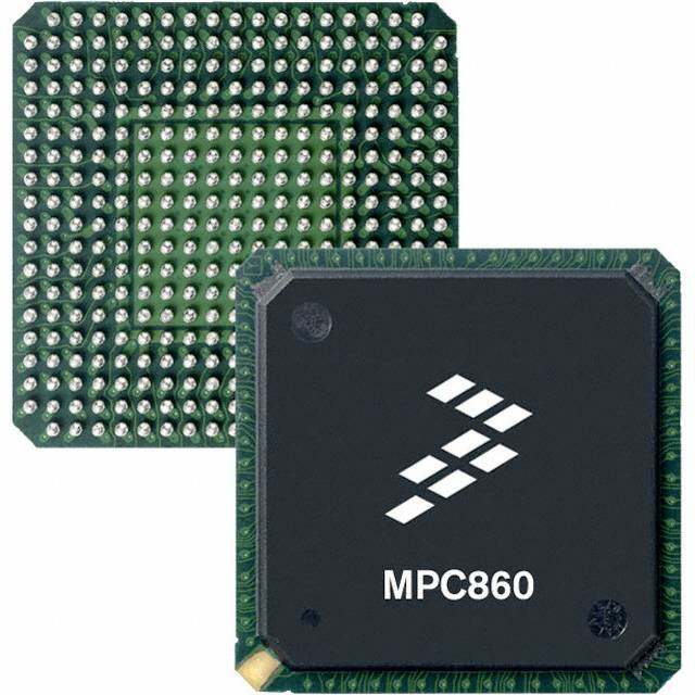
ICGOO电子元器件商城为您提供MPC8275VRMIBA由Freescale Semiconductor设计生产,在icgoo商城现货销售,并且可以通过原厂、代理商等渠道进行代购。 MPC8275VRMIBA价格参考¥900.44-¥1146.01。Freescale SemiconductorMPC8275VRMIBA封装/规格:嵌入式 - 微处理器, PowerPC G2_LE Microprocessor IC MPC82xx 1 Core, 32-Bit 266MHz 516-FPBGA (27x27)。您可以下载MPC8275VRMIBA参考资料、Datasheet数据手册功能说明书,资料中有MPC8275VRMIBA 详细功能的应用电路图电压和使用方法及教程。
NXP USA Inc. 生产的MPC8275VRMIBA是一款嵌入式微处理器,广泛应用于工业控制、通信基础设施和网络设备等领域。以下是其主要应用场景:

1. 工业自动化:MPC8275VRMIBA具备高性能计算能力和丰富的外设接口,适用于工业自动化控制系统。它可以用于PLC(可编程逻辑控制器)、SCADA(数据采集与监控系统)等设备中,实现对生产过程的精确控制和实时监测。

2. 通信设备:该微处理器支持多种通信协议,适合用于路由器、交换机和其他网络设备。它能够处理复杂的通信任务,如数据包转发、路由选择和流量管理,确保网络的高效运行。

3. 嵌入式系统开发:MPC8275VRMIBA具有强大的处理能力和灵活性,是开发复杂嵌入式系统的理想选择。它可以用于开发定制化的嵌入式应用,如医疗设备、汽车电子和智能家居产品。

4. 网络安全设备:该处理器支持硬件加密加速功能,适用于防火墙、入侵检测系统等网络安全设备。它可以通过快速处理加密和解密操作,提高数据传输的安全性和效率。

5. 多媒体处理:MPC8275VRMIBA具备多媒体处理能力,可用于视频编码、解码和图像处理。它适用于数字标牌、视频会议系统和监控摄像头等应用。

6. 军事和航空航天:由于其高可靠性和稳定性,MPC8275VRMIBA在军事和航空航天领域也有广泛应用。它可以用于导航系统、雷达设备和飞行控制系统等关键任务中,确保系统的稳定性和安全性。

总之,MPC8275VRMIBA凭借其高性能、低功耗和丰富的外设接口,成为多个领域的理想选择,特别适合需要高性能计算和实时处理的应用场景。
| 参数 | 数值 |
| AdditionalInterfaces | I²C, SCC, SMC, SPI, UART, USART |
| 产品目录 | 集成电路 (IC) |
| Co-Processors/DSP | Communications; RISC CPM |
| 描述 | IC MPU POWERQUICC II 516-PBGA |
| Display&InterfaceControllers | - |
| 产品分类 | |
| GraphicsAcceleration | No |
| 品牌 | Freescale Semiconductor |
| NumberofCores/BusWidth | 1 Core, 32-Bit |
| 数据手册 | |
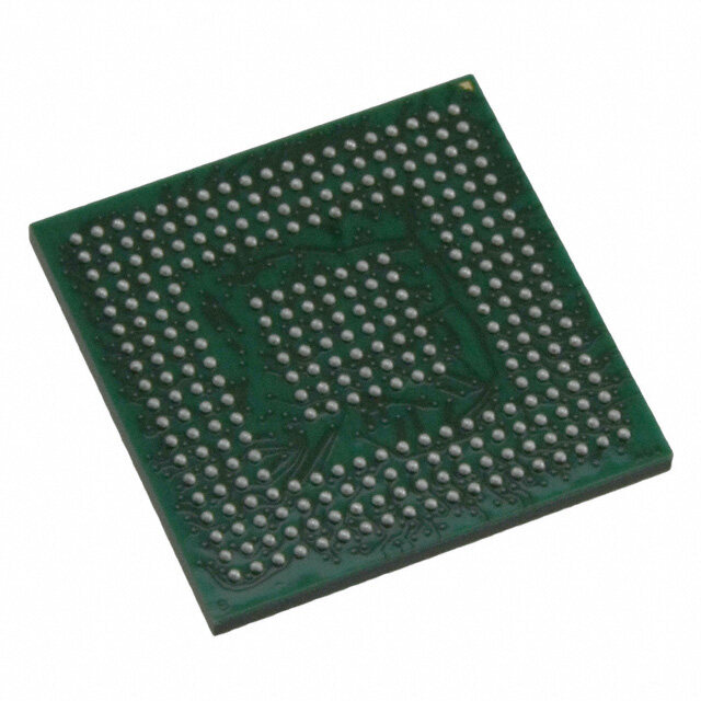
| 产品图片 |
|
| 产品型号 | MPC8275VRMIBA |
| RAMControllers | DRAM, SDRAM |
| RAM控制器 | DRAM, SDRAM |
| rohs | 无铅 / 符合限制有害物质指令(RoHS)规范要求 |
| SATA | - |
| SecurityFeatures | - |
| 产品系列 | MPC82xx |
| USB | USB 2.0(1) |
| 以太网 | 10/100 Mbps (3) |
| 供应商器件封装 | 516-FPBGA(27x27) |
| 包装 | 托盘 |
| 协处理器/DSP | 通信; RISC CPM |
| 图形加速 | 无 |
| 处理器类型 | 32-位 MPC82xx PowerQUICC II |
| 安全特性 | - |
| 安装类型 | 表面贴装 |
| 封装/外壳 | 516-BBGA |
| 工作温度 | 0°C ~ 105°C |
| 显示与接口控制器 | - |
| 标准包装 | 80 |
| 核心处理器 | PowerPC G2_LE |
| 核数/总线宽度 | 1 코어, 32 位 |
| 特性 | - |
| 电压 | 1.5V |
| 电压-I/O | 3.3V |
| 速度 | 266MHz |
| 附加接口 | I²C, SCC, SMC, SPI, UART, USART |


- 商务部:美国ITC正式对集成电路等产品启动337调查
- 曝三星4nm工艺存在良率问题 高通将骁龙8 Gen1或转产台积电
- 太阳诱电将投资9.5亿元在常州建新厂生产MLCC 预计2023年完工
- 英特尔发布欧洲新工厂建设计划 深化IDM 2.0 战略
- 台积电先进制程称霸业界 有大客户加持明年业绩稳了
- 达到5530亿美元!SIA预计今年全球半导体销售额将创下新高
- 英特尔拟将自动驾驶子公司Mobileye上市 估值或超500亿美元
- 三星加码芯片和SET,合并消费电子和移动部门,撤换高东真等 CEO
- 三星电子宣布重大人事变动 还合并消费电子和移动部门
- 海关总署:前11个月进口集成电路产品价值2.52万亿元 增长14.8%
PDF Datasheet 数据手册内容提取
Freescale Semiconductor Document Number: MPC8280EC Rev. 2, 09/2011 Technical Data MPC8280 PowerQUICC II Family Hardware Specifications This document contains detailed information about power Contents considerations, DC/AC electrical characteristics, and AC 1. Overview . . . . . . . . . . . . . . . . . . . . . . . . . . . . . . . . . . . 2 2. Operating Conditions . . . . . . . . . . . . . . . . . . . . . . . . . 7 timing specifications for .13µm (HiP7) members of the 3. DC Electrical Characteristics . . . . . . . . . . . . . . . . . . . 9 PowerQUICCII family of integrated communications 4. Thermal Characteristics . . . . . . . . . . . . . . . . . . . . . . 12 processors—the MPC8280, the MPC8275, and the 5. Power Dissipation . . . . . . . . . . . . . . . . . . . . . . . . . . . 15 6. AC Electrical Characteristics . . . . . . . . . . . . . . . . . . 16 MPC8270 (collectively called the MPC8280 throughout this 7. Clock Configuration Modes . . . . . . . . . . . . . . . . . . . 26 document). 8. Pinout . . . . . . . . . . . . . . . . . . . . . . . . . . . . . . . . . . . . 45 9. Package Description . . . . . . . . . . . . . . . . . . . . . . . . . 75 10. Ordering Information . . . . . . . . . . . . . . . . . . . . . . . . 79 11. Document Revision History . . . . . . . . . . . . . . . . . . . 79 ©2011 Freescale Semiconductor, Inc. All rights reserved.
Overview 1 Overview This table shows the functionality supported by each SoC in the MPC8280 family. Table1. MPC8280 PowerQUICC II Family Functionality SoCs Functionality MPC8270 MPC8275 MPC8280 Package1 480 TBGA 516 PBGA 516 PBGA 480 TBGA Serial communications controllers (SCCs) 4 4 4 4 QUICC multi-channel controller (QMC) — — — — Fast communication controllers (FCCs) 3 3 3 3 I-Cache (Kbyte) 16 16 16 16 D-Cache (Kbyte) 16 16 16 16 Ethernet (10/100) 3 3 3 3 UTOPIA II Ports 0 0 2 2 Multi-channel controllers (MCCs) 1 1 1 2 PCI bridge Yes Yes Yes Yes Transmission convergence (TC) layer — — — Yes Inverse multiplexing for ATM (IMA) — — — Yes Universal serial bus (USB) 2.0 full/low rate 1 1 1 1 Security engine (SEC) — — — — 1 See Table2. Devices in the MPC8280 family are available in four packages—the standard ZU and VV packages and the alternate VR or ZQ packages—as shown in Table2. Note that throughout this document, references to the MPC8280 and the MPC8270 are inclusive of VR and ZQ package devices unless otherwise specified. For more information on VR and ZQ packages, contact your Freescale sales office. For package ordering information, see Section10, “Ordering Information.” Table2. HiP7 PowerQUICC II Device Packages Code ZU VV VR ZQ (Package) (480 TBGA—Leaded) (480 TBGA—Lead Free) (516 PBGA—Lead free) (516 PBGA—Lead spheres) MPC8280 MPC8280 MPC8275VR MPC8275ZQ Device MPC8270 MPC8270 MPC8270VR MPC8270ZQ MPC8280 PowerQUICC II Family Hardware Specifications, Rev. 2 2 Freescale Semiconductor
Overview This figure shows the block diagram of the SoC. Shaded portions are SoC-specific; see the notes below the figure. 16 KB I-Cache I-MMU System Interface Unit (SIU) 60x Bus G2_LE Core 16 KB Bus Interface Unit D-Cache PCI Bus D-MMU 60x-to-PCI 32 bits, up to 66 MHz Bridge or 60x-to-Local Local Bus Bridge Communication Processor Module (CPM) 32 bits, up to 100 MHz Memory Controller 32 KB 32 KB Timers Interrupt Instruction Data Serial Controller RAM RAM DMAs Clock Counter Parallel I/O 32-bit RISC Microcontroller 4 Virtual System Functions Baud Rate and Program ROM IDMAs Generators IMA1 Microcode MCC11 MCC2 FCC1 FCC2 FCC3 SCC1 SCC2 SCC3 SCC4/ SMC1 SMC2 SPI I2C USB TC Layer Hardware1 Time Slot Assigner Serial Interface2 8 TDM Ports2 3 MII or RMII 2 UTOPIA Non-Multiplexed Ports Ports3 I/O Notes: 1 MPC8280 only (not on MPC8270, the VR package, nor the ZQ package) 2 MPC8280 has 2 serial interface (SI) blocks and 8 TDM ports. MPC8270 and the VR and ZQ packages have only 1 SI block and 4 TDM ports (TDM2[A–D]). 3 MPC8280, MPC8275VR, MPC8275ZQ only (not on MPC8270, MPC8270VR, nor MPC8270ZQ) Figure1. SoC Block Diagram 1.1 Features The major features of the SoC are as follows: (cid:129) Dual-issue integer (G2_LE) core — A core version of the EC603e microprocessor — System core microprocessor supporting frequencies of 166–450 MHz — Separate 16 KB data and instruction caches: – Four-way set associative – Physically addressed – LRU replacement algorithm — Power Architecture®-compliant memory management unit (MMU) MPC8280 PowerQUICC II Family Hardware Specifications, Rev. 2 Freescale Semiconductor 3
Overview — Common on-chip processor (COP) test interface — High-performance (SPEC95 benchmark at 450 MHz; 855 Dhrystones MIPS at 450MHz) — Supports bus snooping — Support for data cache coherency — Floating-point unit (FPU) (cid:129) Separate power supply for internal logic and for I/O (cid:129) Separate PLLs for G2_LE core and for the communications processor module (CPM) — G2_LE core and CPM can run at different frequencies for power/performance optimization — Internal core/bus clock multiplier that provides ratios 2:1, 2.5:1, 3:1, 3.5:1, 4:1, 4.5:1, 5:1, 6:1, 7:1, 8:1 — Internal CPM/bus clock multiplier that provides ratios 2:1, 2.5:1, 3:1, 3.5:1, 4:1, 5:1, 6:1, 8:1 ratios (cid:129) 64-bit data and 32-bit address 60x bus — Bus supports multiple master designs — Supports single- and four-beat burst transfers — 64-, 32-, 16-, and 8-bit port sizes controlled by on-chip memory controller — Supports data parity or ECC and address parity (cid:129) 32-bit data and 18-bit address local bus — Single-master bus, supports external slaves — Eight-beat burst transfers — 32-, 16-, and 8-bit port sizes controlled by on-chip memory controller (cid:129) 60x-to-PCI bridge — Programmable host bridge and agent — 32-bit data bus, 66.67/83.3/100 MHz, 3.3 V — Synchronous and asynchronous 60x and PCI clock modes — All internal address space available to external PCI host — DMA for memory block transfers — PCI-to-60x address remapping (cid:129) PCI bridge — PCI Specification Revision 2.2 compliant and supports frequencies up to 66 MHz — On-chip arbitration — Support for PCI-to-60x-memory and 60x-memory-to-PCI streaming — PCI host bridge or peripheral capabilities — Includes 4 DMA channels for the following transfers: – PCI-to-60x to 60x-to-PCI – 60x-to-PCI to PCI-to-60x – 60x-to-PCI to 60x-to-PCI MPC8280 PowerQUICC II Family Hardware Specifications, Rev. 2 4 Freescale Semiconductor
Overview — Includes all of the configuration registers (which are automatically loaded from the EPROM and used to configure the MPC8280) required by the PCI standard as well as message and doorbell registers — Supports the I O standard 2 — Hot-swap friendly (supports the hot swap specification as defined by PICMG 2.1 R1.0 August 3, 1998) — Support for 66.67/83.33/100 MHz, 3.3 V specification — 60x-PCI bus core logic that uses a buffer pool to allocate buffers for each port — Uses the local bus signals, removing need for additional pins (cid:129) System interface unit (SIU) — Clock synthesizer — Reset controller — Real-time clock (RTC) register — Periodic interrupt timer — Hardware bus monitor and software watchdog timer — IEEE 1149.1 JTAG test access port (cid:129) 12-bank memory controller — Glueless interface to SRAM, page mode SDRAM, DRAM, EPROM, Flash, and other user-definable peripherals — Byte write enables and selectable parity generation — 32-bit address decodes with programmable bank size — Three user-programmable machines, general-purpose chip-select machine, and page mode pipeline SDRAM machine — Byte selects for 64-bit bus width (60x) and byte selects for 32-bus width (local) — Dedicated interface logic for SDRAM (cid:129) CPU core can be disabled and the device can be used in slave mode to an external core (cid:129) Communications processor module (CPM) — Embedded 32-bit communications processor (CP) uses a RISC architecture for flexible support for communications protocols — Interfaces to G2_LE core through an on-chip 32 KB dual-port data RAM, an on-chip 32 KB dual-port instruction RAM and DMA controller — Serial DMA channels for receive and transmit on all serial channels — Parallel I/O registers with open-drain and interrupt capability — Virtual DMA functionality executing memory-to-memory and memory-to-I/O transfers — Three fast communications controllers supporting the following protocols: – 10/100-Mbit Ethernet/IEEE 802.3 CDMA/CS interface through media independent interface (MII) or reduced media independent interface (RMII) MPC8280 PowerQUICC II Family Hardware Specifications, Rev. 2 Freescale Semiconductor 5
Overview – ATM—Full-duplex SAR protocols at 155 Mbps, through UTOPIA interface, AAL5, AAL1, AAL0 protocols, TM 4.0 CBR, VBR, UBR, ABR traffic types, up to 64 K external connections (no ATM support for the MPC8270) – Transparent – HDLC—Up to T3 rates (clear channel) – FCC2 can also be connected to the TC layer (MPC8280 only) — Two multichannel controllers (MCCs) (one MCC on the MPC8270) – Each MCC handles 128 serial, full-duplex, 64-Kbps data channels. Each MCC can be split into four subgroups of 32 channels each. – Almost any combination of subgroups can be multiplexed to single or multiple TDM interfaces up to four TDM interfaces per MCC — Four serial communications controllers (SCCs) identical to those on the MPC860, supporting the digital portions of the following protocols: – Ethernet/IEEE 802.3 CDMA/CS – HDLC/SDLC and HDLC bus – Universal asynchronous receiver transmitter (UART) – Synchronous UART – Binary synchronous (BISYNC) communications – Transparent (cid:129) Universal serial bus (USB) controller — Supports USB 2.0 full/low rate compatible — USB host mode – Supports control, bulk, interrupt, and isochronous data transfers – CRC16 generation and checking – NRZI encoding/decoding with bit stuffing – Supports both 12- and 1.5-Mbps data rates (automatic generation of preamble token and data rate configuration). Note that low-speed operation requires an external hub. – Flexible data buffers with multiple buffers per frame – Supports local loopback mode for diagnostics (12 Mbps only) — Supports USB slave mode – Four independent endpoints support control, bulk, interrupt, and isochronous data transfers – CRC16 generation and checking – CRC5 checking – NRZI encoding/decoding with bit stuffing – 12- or 1.5-Mbps data rate – Flexible data buffers with multiple buffers per frame – Automatic retransmission upon transmit error — Two serial management controllers (SMCs), identical to those of the MPC860 MPC8280 PowerQUICC II Family Hardware Specifications, Rev. 2 6 Freescale Semiconductor
Operating Conditions – Provides management for BRI devices as general-circuit interface (GCI) controllers in time-division-multiplexed (TDM) channels – Transparent – UART (low-speed operation) — One serial peripheral interface identical to the MPC860 SPI — One I2C controller (identical to the MPC860 I2C controller) – Microwire compatible – Multiple-master, single-master, and slave modes — Up to eight TDM interfaces (four on the MPC8270) – Supports two groups of four TDM channels for a total of eight TDMs (one group of four on the MPC8270 and the MPC8275) – 2,048 bytes of SI RAM – Bit or byte resolution – Independent transmit and receive routing, frame synchronization – Supports T1, CEPT, T1/E1, T3/E3, pulse code modulation highway, ISDN basic rate, ISDN primary rate, Freescale interchip digital link (IDL), general circuit interface (GCI), and user-defined TDM serial interfaces — Eight independent baud rate generators and 20 input clock pins for supplying clocks to FCCs, SCCs, SMCs, and serial channels — Four independent 16-bit timers that can be interconnected as two 32-bit timers (cid:129) Inverse multiplexing for ATM capabilities (IMA) (MPC8280 only). Supported by eight transfer transmission convergence (TC) layers between the TDMs and FCC2. (cid:129) Transmission convergence (TC) layer (MPC8280 only) 2 Operating Conditions This table shows the maximum electrical ratings. Table3. Absolute Maximum Ratings1 Rating Symbol Value Unit Core supply voltage2 VDD –0.3 – 2.25 V PLL supply voltage2 VCCSYN –0.3 – 2.25 V I/O supply voltage3 VDDH –0.3 – 4.0 V Input voltage4 VIN GND(–0.3) – 3.6 V Junction temperature T 120 °C j Storage temperature range T (–55) – (+150) °C STG 1 Absolute maximum ratings are stress ratings only; functional operation (see Table4) at the maximums is not guaranteed. Stress beyond those listed may affect device reliability or cause permanent damage. MPC8280 PowerQUICC II Family Hardware Specifications, Rev. 2 Freescale Semiconductor 7
Operating Conditions 2 Caution: VDD/VCCSYN must not exceed VDDH by more than 0.4 V during normal operation. It is recommended that VDD/VCCSYN should be raised before or simultaneous with VDDH during power-on reset. VDD/VCCSYN may exceed VDDH by more than 0.4 V during power-on reset for no more than 100 ms. 3 Caution: VDDH can exceed VDD/VCCSYN by 3.3 V during power on reset by no more than 100 mSec. VDDH should not exceed VDD/VCCSYN by more than 2.5V during normal operation. 4 Caution: VIN must not exceed VDDH by more than 2.5 V at any time, including during power-on reset. This table lists recommended operational voltage conditions. Table4. Recommended Operating Conditions1 Rating Symbol Value Unit Core supply voltage VDD 1.45 – 1.60 V PLL supply voltage VCCSYN 1.45 – 1.60 V I/O supply voltage VDDH 3.135 – 3.465 V Input voltage VIN GND (–0.3) – 3.465 V Junction temperature (maximum) T 1052 °C j Ambient temperature T 0–702 °C A 1 Caution: These are the recommended and tested operating conditions. Proper operation outside of these conditions is not guaranteed. 2 Note that for extended temperature parts the range is (-40) – 105 . TA Tj This SoC contains circuitry protecting against damage due to high static voltage or electrical fields; however, it is advised that normal precautions be taken to avoid application of any voltages higher than maximum-rated voltages to this high-impedance circuit. Reliability of operation is enhanced if unused inputs are tied to an appropriate logic voltage level (either GND or V ). CC This figure shows the undershoot and overshoot voltage of the 60x and local bus memory interface of the SoC. Note that in PCI mode the I/O interface is different. 4 V GV + 5% DD V GV IH DD GND GND – 0.3 V V IL GND – 1.0 V Not to exceed 10% of t SDRAM_CLK Figure2. Overshoot/Undershoot Voltage MPC8280 PowerQUICC II Family Hardware Specifications, Rev. 2 8 Freescale Semiconductor
DC Electrical Characteristics 3 DC Electrical Characteristics This table shows DC electrical characteristics. Table5. DC Electrical Characteristics1 Characteristic Symbol Min Max Unit Input high voltage—all inputs except TCK, TRST and PORESET2 V 2.0 3.465 V IH Input low voltage V GND 0.8 V IL CLKIN input high voltage V 2.4 3.465 V IHC CLKIN input low voltage V GND 0.4 V ILC Input leakage current, V = VDDH3 I — 10 µA IN IN Hi-Z (off state) leakage current, V = VDDH3 I — 10 µA IN OZ Signal low input current, V = 0.8 V4 I — 1 µA IL L Signal high input current, V = 2.0 V I — 1 µA IH H Output high voltage, I = –2 mA V 2.4 — V OH OH except UTOPIA mode, and open drain pins In UTOPIA mode5 (UTOPIA pins only): I = -8.0mA OH PA[0-31] PB[4-31] PC[0-31] PD[4-31] In UTOPIA mode5 (UTOPIA pins only): I = 8.0mA V — 0.5 V OL OL PA[0-31] PB[4-31] PC[0-31] PD[4-31] MPC8280 PowerQUICC II Family Hardware Specifications, Rev. 2 Freescale Semiconductor 9
DC Electrical Characteristics Table5. DC Electrical Characteristics1 (continued) Characteristic Symbol Min Max Unit I = 6.0mA V — 0.4 V OL OL BR BG ABB/IRQ2 TS A[0-31] TT[0-4] TBST TSIZE[0–3] AACK ARTRY DBG DBB/IRQ3 D[0-63] DP(0)/RSRV/EXT_BR2 DP(1)/IRQ1/EXT_BG2 DP(2)/TLBISYNC/IRQ2/EXT_DBG2 DP(3)/IRQ3/EXT_BR3/CKSTP_OUT DP(4)/IRQ4/EXT_BG3/CORE_SREST DP(5)/TBEN/EXT_DBG3/IRQ5/CINT DP(6)/CSE(0)/IRQ6 DP(7)/CSE(1)/IRQ7 PSDVAL TA TEA GBL/IRQ1 CI/BADDR29/IRQ2 WT/BADDR30/IRQ3 L2_HIT/IRQ4 CPU_BG/BADDR31/IRQ5/CINT CPU_DBG CPU_BR IRQ0/NMI_OUT IRQ7/PCI_RSTINT_OUT/APE PORESET HRESET SRESET RSTCONF MPC8280 PowerQUICC II Family Hardware Specifications, Rev. 2 10 Freescale Semiconductor
DC Electrical Characteristics Table5. DC Electrical Characteristics1 (continued) Characteristic Symbol Min Max Unit I = 5.3mA V — 0.4 V OL OL CS[0-9] CS(10)/BCTL1 CS(11)/AP(0) BADDR[27–28] ALE BCTL0 PWE[0–7]/PSDDQM[0–7]/PBS[0–7] PSDA10/PGPL0 PSDWE/PGPL1 POE/PSDRAS/PGPL2 PSDCAS/PGPL3 PGTA/PUPMWAIT/PGPL4/PPBS PSDAMUX/PGPL5 LWE[0–3]LSDDQM[0–3]/LBS[0–3]/PCI_CFG[0–3] LSDA10/LGPL0/PCI_MODCKH0 LSDWE/LGPL1/PCI_MODCKH1 LOE/LSDRAS/LGPL2/PCI_MODCKH2 LSDCAS/LGPL3/PCI_MODCKH3 LGTA/LUPMWAIT/LGPL4/LPBS LSDAMUX/LGPL5/PCI_MODCK LWR MODCK[1–3]/AP[1–3]/TC[0–2]/BNKSEL[0–2] I = 3.2mA OL L_A14/PAR L_A15/FRAME/SMI L_A16/TRDY L_A17/IRDY/CKSTP_OUT L_A18/STOP L_A19/DEVSEL L_A20/IDSEL L_A21/PERR L_A22/SERR L_A23/REQ0 L_A24/REQ1/HSEJSW L_A25/GNT0 L_A26/GNT1/HSLED L_A27/GNT2/HSENUM L_A28/RST/CORE_SRESET L_A29/INTAL_A30/REQ2 L_A31 LCL_D[0-31)]/AD[0-31] LCL_DP[03]/C/BE[0-3] PA[0–31] PB[4–31] PC[0–31] PD[4–31] TDO QREQ 1 The default configuration of the CPM pins (PA[0–31], PB[4–31], PC[0–31], PD[4–31]) is input. To prevent excessive DC current, either pull unused pins to GND or VDDH or configure them as outputs. 2 TCK, TRST and PORESET have min VIH = 2.5V. 3 The leakage current is measured for nominal VDDH,VCCSYN, and VDD. MPC8280 PowerQUICC II Family Hardware Specifications, Rev. 2 Freescale Semiconductor 11
Thermal Characteristics 4 V for IIC interface does not match IIC standard, but does meet IIC standard for V and should not cause any compatibility IL OL issue. 5 MPC8280, MPC8275VR, MPC8275ZQ only. 4 Thermal Characteristics This table describes thermal characteristics for both the packages. See Table 2 for information on a given SoC’s package. Discussions of each characteristic are provided in Section4.1, “Estimation with Junction-to-Ambient Thermal Resistance,” and Section 4.5, “Experimental Determination.” For the these discussions, P = (V × I ) + PI/O, where PI/O is the power dissipation of the I/O drivers. D DD DD Table6. Thermal Characteristics Value Characteristic Symbol Unit Air Flow 480 TBGA 516 PBGA Junction to ambient— 16 27 Natural convection single-layer board1 RθJA °C/W 11 21 1 m/s Junction to ambient— 12 19 Natural convection four-layer board RθJA °C/W 9 16 1 m/s Junction to board2 RθJB 6 11 °C/W — Junction to case3 RθJC 2 8 °C/W — Junction-to-package top4 Ψ 2 2 °C/W — JT 1 Assumes no thermal vias 2 Thermal resistance between the die and the printed circuit board per JEDEC JESD51-8. Board temperature is measured on the top surface of the board near the package. 3 Thermal resistance between the die and the case top surface as measured by the cold plate method (MIL SPEC-883 Method 1012.1). 4 Thermal characterization parameter indicating the temperature difference between package top and the junction temperature per JEDEC JESD51-2. When Greek letters are not available, the thermal characterization parameter is written as Psi-JT. 4.1 Estimation with Junction-to-Ambient Thermal Resistance An estimation of the chip junction temperature, T , in (cid:31) C can be obtained from the following equation: J TJ = TA + (RθJA × PD) where: T = ambient temperature (ºC) A RθJA = package junction-to-ambient thermal resistance (ºC/W) P = power dissipation in package D The junction-to-ambient thermal resistance is an industry standard value that provides a quick and easy estimation of thermal performance. However, the answer is only an estimate; test cases have demonstrated that errors of a factor of two (in the quantity T – T ) are possible. J A MPC8280 PowerQUICC II Family Hardware Specifications, Rev. 2 12 Freescale Semiconductor
Thermal Characteristics 4.2 Estimation with Junction-to-Case Thermal Resistance Historically, the thermal resistance has frequently been expressed as the sum of a junction-to-case thermal resistance and a case-to-ambient thermal resistance: RθJA = RθJC + RθCA where: RθJA = junction-to-ambient thermal resistance (ºC/W) RθJC = junction-to-case thermal resistance (ºC/W) RθCA = case-to-ambient thermal resistance (ºC/W) RθJC is device related and cannot be influenced by the user. The user adjusts the thermal environment to affect the case-to-ambient thermal resistance, RθCA. For instance, the user can change the air flow around the device, add a heat sink, change the mounting arrangement on the printed circuit board, or change the thermal dissipation on the printed circuit board surrounding the device. This thermal model is most useful for ceramic packages with heat sinks where some 90% of the heat flows through the case and the heat sink to the ambient environment. For most packages, a better model is required. 4.3 Estimation with Junction-to-Board Thermal Resistance A simple package thermal model which has demonstrated reasonable accuracy (about 20%) is a two-resistor model consisting of a junction-to-board and a junction-to-case thermal resistance. The junction-to-case thermal resistance covers the situation where a heat sink is used or where a substantial amount of heat is dissipated from the top of the package. The junction-to-board thermal resistance describes the thermal performance when most of the heat is conducted to the printed circuit board. It has been observed that the thermal performance of most plastic packages, especially PBGA packages, is strongly dependent on the board temperature. If the board temperature is known, an estimate of the junction temperature in the environment can be made using the following equation: TJ = TB + (RθJB × PD) where: RθJB = junction-to-board thermal resistance (ºC/W) T = board temperature (ºC) B P = power dissipation in package D If the board temperature is known and the heat loss from the package case to the air can be ignored, acceptable predictions of junction temperature can be made. For this method to work, the board and board mounting must be similar to the test board used to determine the junction-to-board thermal resistance, namely a 2s2p (board with a power and a ground plane) and by attaching the thermal balls to the ground plane. MPC8280 PowerQUICC II Family Hardware Specifications, Rev. 2 Freescale Semiconductor 13
Thermal Characteristics 4.4 Estimation Using Simulation When the board temperature is not known, a thermal simulation of the application is needed. The simple two-resistor model can be used with the thermal simulation of the application, or a more accurate and complex model of the package can be used in the thermal simulation. 4.5 Experimental Determination To determine the junction temperature of the device in the application after prototypes are available, the thermal characterization parameter (Ψ ) can be used to determine the junction temperature with a JT measurement of the temperature at the top center of the package case using the following equation: T = T + (Ψ × P ) J T JT D where: Ψ = thermal characterization parameter JT T = thermocouple temperature on top of package T P = power dissipation in package D The thermal characterization parameter is measured per JEDEC JESD51-2 specification using a 40-gauge typeT thermocouple epoxied to the top center of the package case. The thermocouple should be positioned so that the thermocouple junction rests on the package. A small amount of epoxy is placed over the thermocouple junction and over 1 mm of wire extending from the junction. The thermocouple wire is placed flat against the case to avoid measurement errors caused by cooling effects of the thermocouple wire. 4.6 Layout Practices Each VDD and VDDH pin should be provided with a low-impedance path to the board’s power supplies. Each ground pin should likewise be provided with a low-impedance path to ground. The power supply pins drive distinct groups of logic on chip. The VDD and VDDH power supplies should be bypassed to ground using bypass capacitors located as close as possible to the four sides of the package. For filtering high frequency noise, a capacitor of 0.1uF on each VDD and VDDH pin is recommended. Further, for medium frequency noise, a total of 2 capacitors of 47uF for VDD and 2 capacitors of 47uF for VDDH are also recommended. The capacitor leads and associated printed circuit traces connecting to chip VDD, VDDH and ground should be kept to less than half an inch per capacitor lead. Boards should employ separate inner layers for power and GND planes. All output pins on the SoC have fast rise and fall times. Printed circuit (PC) trace interconnection length should be minimized to minimize overdamped conditions and reflections caused by these fast output switching times. This recommendation particularly applies to the address and data buses. Maximum PC trace lengths of six inches are recommended. Capacitance calculations should consider all device loads as well as parasitic capacitances due to the PC traces. Attention to proper PCB layout and bypassing becomes especially critical in systems with higher capacitive loads because these loads create higher transient currents in the VDD and GND circuits. Pull up all unused inputs or signals that will be inputs during reset. Special care should be taken to minimize the noise levels on the PLL supply pins. MPC8280 PowerQUICC II Family Hardware Specifications, Rev. 2 14 Freescale Semiconductor
Power Dissipation 5 Power Dissipation This table provides preliminary, estimated power dissipation for various configurations. Note that suitable thermal management is required to ensure the junction temperature does not exceed the maximum specified value. Also note that the I/O power should be included when determining whether to use a heat sink. For a complete list of possible clock configurations, see Section 7, “Clock Configuration Modes.” Table7. Estimated Power Dissipation for Various Configurations1 P (W)2,3 INT CPM CPU Bus CPM CPU Multiplication Multiplication Vddl 1.5 Volts (MHz) (MHz) (MHz) Factor Factor Nominal Maximum 66.67 2.5 166 3.5 233 0.95 1.0 66.67 2.5 166 4 266 1.0 1.05 66.67 3 200 4 266 1.05 1.1 66.67 3.5 233 4.5 300 1.05 1.15 83.33 3 250 4 333 1.25 1.35 83.33 3 250 4.5 375 1.3 1.4 83.33 3.5 292 5 417 1.45 1.55 100 3 300 4 400 1.5 1.6 100 3 300 4.5 450 1.55 1.65 1 Test temperature = 105° C 2 P = I x V Watts INT DD DD 3 Values do not include I/O. Add the following estimates for active I/O based on the following bus speeds: 66.7 MHz = 0.45 W (nominal), 0.5 W (maximum) 83.3 MHz = 0.5W (nominal), 0.6 W (maximum) 100 MHz = 0.6 W (nominal), 0.7 W (maximum) MPC8280 PowerQUICC II Family Hardware Specifications, Rev. 2 Freescale Semiconductor 15
AC Electrical Characteristics 6 AC Electrical Characteristics The following sections include illustrations and tables of clock diagrams, signals, and CPM outputs and inputs for 66.67/83.33/100 MHz devices. Note that AC timings are based on a 50-pf load for MAX Delay and 10-pf load for MIN delay. Typical output buffer impedances are shown in this table. Table8. Output Buffer Impedances1 Output Buffers Typical Impedance (Ω) 60x bus 45 or 272 Local bus 45 Memory controller 45 or 272 Parallel I/O 45 PCI 27 1 These are typical values at 65° C. Impedance may vary by ±25% with process and temperature. 2 On silicon revision 0.0 (mask #: 0K49M), selectable impedance is not available. Impedance is set at 45 Ω. On all other revisions, impedance value is selected through the SIUMCR[20,21]. See the SoC reference manual. 6.1 CPM AC Characteristics This table lists CPM output characteristics. Table9. AC Characteristics for CPM Outputs1 Spec Number Characteristic Value (ns) Max Min Maximum Delay Minimum Delay 66 MHz 83 MHz 100 MHz 66 MHz 83 MHz 100 MHz sp36a sp37a FCC outputs—internal clock (NMSI) 6 5.5 5.5 0.5 0.5 0.5 sp36b sp37b FCC outputs—external clock (NMSI) 8 8 8 2 2 2 sp38a sp39a SCC/SMC/SPI/I2C outputs—internal 10 10 10 0 0 0 clock (NMSI) sp38b sp39b SCC/SMC/SPI/I2C outputs—external 8 8 8 2 2 2 clock (NMSI) sp40 sp41 TDM outputs/SI 11 11 11 2.5 2.5 2.5 sp42 sp43 TIMER/IDMA outputs 11 11 11 0.5 0.5 0.5 sp42a sp43a PIO outputs 11 11 11 0.5 0.5 0.5 1 Output specifications are measured from the 50% level of the rising edge of CLKIN to the 50% level of the signal. Timings are measured at the pin. MPC8280 PowerQUICC II Family Hardware Specifications, Rev. 2 16 Freescale Semiconductor
AC Electrical Characteristics This table lists CPM input characteristics. NOTE: Rise/Fall Time on CPM Input Pins It is recommended that the rise/fall time on CPM input pins should not exceed 5 ns. This should be enforced especially on clock signals. Rise time refers to signal transitions from 10% to 90% of VCC; fall time refers to transitions from 90% to 10% of VCC. Table10. AC Characteristics for CPM Inputs1 Spec Number Value (ns) Setup Hold Characteristic Setup Hold 66 MHz 83 MHz 100 MHz 66 MHz 83 MHz 100 MHz sp16a sp17a FCC inputs—internal clock (NMSI) 6 6 6 0 0 0 sp16b sp17b FCC inputs—external clock (NMSI) 2.5 2.5 2.5 2 2 2 sp18a sp19a SCC/SMC/SPI/I2C inputs—internal clock 6 6 6 0 0 0 (NMSI) sp18b sp19b SCC/SMC/SPI/I2C inputs—external clock 4 4 4 2 2 2 (NMSI) sp20 sp21 TDM inputs/SI 5 5 5 2.5 2.5 2.5 sp22 sp23 PIO/TIMER/IDMA inputs 8 8 8 0.5 0.5 0.5 1 Input specifications are measured from the 50% level of the signal to the 50% level of the rising edge of CLKIN. Timings are measured at the pin. NOTE Although the specifications generally reference the rising edge of the clock, the following AC timing diagrams also apply when the falling edge is the active edge. This figure shows the FCC internal clock. BRG_OUT sp17a sp16a FCC input signals sp36a/sp37a FCC output signals Note: When GFMR[TCI] = 0 sp36a/sp37a FCC output signals Note: When GFMR.[TCI] = 1 Figure3. FCC Internal Clock Diagram MPC8280 PowerQUICC II Family Hardware Specifications, Rev. 2 Freescale Semiconductor 17
AC Electrical Characteristics This figure shows the FCC external clock. Serial ClKin sp17b sp16b FCC input signals sp36b/sp37b FCC output signals No te: When GFMR[TCI] = 0 sp36b/sp37b FCC output signals Note: When GFMR[TCI] = 1 Figure4. FCC External Clock Diagram This figure shows the SCC/SMC/SPI/I2C external clock. Serial CLKin sp18b sp19b SCC/SMC/SPI/I2C input signals (See note) sp38b/sp39b SCC/SMC/SPI/I2C output signals (See note) Note: There are four possible timing conditions for SCC and SPI: 1. Input sampled on the rising edge and output driven on the rising edge (shown). 2. Input sampled on the rising edge and output driven on the falling edge. 3. Input sampled on the falling edge and output driven on the falling edge. 4. Input sampled on the falling edge and output driven on the rising edge. Figure5. SCC/SMC/SPI/I2C External Clock Diagram MPC8280 PowerQUICC II Family Hardware Specifications, Rev. 2 18 Freescale Semiconductor
AC Electrical Characteristics This figure shows the SCC/SMC/SPI/I2C internal clock. BRG_OUT sp18a sp19a SCC/SMC/SPI/I2C input signals (See note) sp38a/sp39a SCC/SMC/SPI/I2C output signals (See note) Note: There are four possible timing conditions for SCC and SPI: 1. Input sampled on the rising edge and output driven on the rising edge (shown). 2. Input sampled on the rising edge and output driven on the falling edge. 3. Input sampled on the falling edge and output driven on the falling edge. 4. Input sampled on the falling edge and output driven on the rising edge. Figure6. SCC/SMC/SPI/I2C Internal Clock Diagram This figure shows TDM input and output signals. Serial CLKin sp20 sp21 TDM input signals sp40/sp41 TDM output signals Note: There are four possible TDM timing conditions: 1. Input sampled on the rising edge and output driven on the rising edge (shown). 2. Input sampled on the rising edge and output driven on the falling edge. 3. Input sampled on the falling edge and output driven on the falling edge. 4. Input sampled on the falling edge and output driven on the rising edge. Figure7. TDM Signal Diagram MPC8280 PowerQUICC II Family Hardware Specifications, Rev. 2 Freescale Semiconductor 19
AC Electrical Characteristics This figure shows PIO and timer signals. Sys clk sp23 sp22 PIO/IDMA/TIMER[TGATE assertion] input signals (See note) sp23 sp22 TIMER input signal [TGATE deassertion] (See note) sp42/sp43 IDMA output signals sp42/sp43 sp42a/sp43a TIMER(sp42/43)/ PIO(sp42a/sp43a) output signals Note: TGATE is asserted on the rising edge of the clock; it is deasserted on the falling edge. Figure8. PIO and Timer Signal Diagram 6.2 SIU AC Characteristics This table lists SIU input characteristics. NOTE: CLKIN Jitter and Duty Cycle The CLKIN input to the SoC should not exceed +/– 150 psec of jitter (peak-to-peak). This represents total input jitter—the combination of short term (cycle-to-cycle) and long term (cumulative). The duty cycle of CLKIN should not exceed the ratio of 40:60. The rise/file time of CLKIN should adhere to the typical SDRAM device AC clock requirement of 1 V/ns to meet SDRAM AC specs. NOTE: Spread Spectrum Clocking Spread spectrum clocking is allowed with 1% input frequency down-spread at maximum 60 KHz modulation rate regardless of input frequency. NOTE: PCI AC Timing The SoC meets the timing requirements of PCI Specification Revision 2.2. See Section 7, “Clock Configuration Modes,” and “Note: Tval (Output Hold)” to determine if a specific clock configuration is compliant. MPC8280 PowerQUICC II Family Hardware Specifications, Rev. 2 20 Freescale Semiconductor
AC Electrical Characteristics NOTE: Conditions The following conditions must be met in order to operate the MPC8272 family devices with 133 MHz bus: single PowerQUICC II Bus mode must be used (no external master, BCR[EBM] = 0); data bus must be in Pipeline mode (BRx[DR]=1); internal arbiter and memory controller must be used. For expected load of above 40 pF, it is recommended that data and address buses be configured to low (25 Ω) impedance (SIUMCR[HLBE0]= 1, SIUMCR[HLBE1] =1). Table11. AC Characteristics for SIU Inputs1 Spec Number Value (ns) Setup Hold Characteristic Setup Hold 66 83 100 133 66 83 100 133 MHz MHz MHz MHz MHz MHz MHz MHz sp11 sp10 AACK/TA/TS/DBG/BG/BR/ARTRY/TEA 6 5 3.5 N/A 0.5 0.5 0.5 N/A sp12 sp10 Data bus in normal mode 5 4 3.5 N/A 0.5 0.5 0.5 N/A sp13 sp10 Data bus in pipeline mode (without ECC and N/A 4 2.5 1.5 N/A 0.5 0.5 0.5 PARITY) sp15 sp10 All other pins 5 4 3.5 N/A 0.5 0.5 0.5 N/A 1 Input specifications are measured from the 50% level of the signal to the 50% level of the rising edge of CLKIN. Timings are measured at the pin. This table lists SIU output characteristics. Table12. AC Characteristics for SIU Outputs1 Spec Number Value (ns) Maximum Delay Minimum Delay Characteristic Max Min 66 83 100 133 66 83 100 133 MHz MHz MHz MHz MHz MHz MHz MHz sp31 sp30 PSDVAL/TEA/TA 7 6 5.5 N/A 1 1 1 N/A sp32 sp30 ADD/ADD_atr./BADDR/CI/GBL/WT 8 6.5 5.5 4.52 1 1 1 1 2 sp33 sp30 Data bus3 6.5 6.5 5.5 4.5 0.8 0.8 0.8 1 sp34 sp30 Memory controller signals/ALE 6 5.5 5.5 4.5 1 1 1 1 sp35 sp30 All other signals 6 5.5 5.5 N/A 1 1 1 N/A 1 Output specifications are measured from the 50% level of the rising edge of CLKIN to the 50% level of the signal. Timings are measured at the pin. 2 Value is for ADD only; other sp32/sp30 signals are not applicable. 3 To achieve 1 ns of hold time at 66.67/83.33/100 MHZ, a minimum loading of 20 pF is required. MPC8280 PowerQUICC II Family Hardware Specifications, Rev. 2 Freescale Semiconductor 21
AC Electrical Characteristics NOTE Activating data pipelining (setting BRx[DR] in the memory controller) improves the AC timing. This table lists SIU input characteristics. Table13. AC Characteristics for SIU Inputs1 Spec Number Value (ns) Setup Hold Characteristic Setup Hold 66 MHz 83 MHz 100 MHz 66 MHz 83 MHz 100 MHz sp11 sp10 AACK/TA/TS/DBG/BG/BR/ARTRY/ 6 5 3.5 0.5 0.5 0.5 TEA sp12 sp10 Data bus in normal mode 5 4 3.5 0.5 0.5 0.5 sp13 sp10 Data bus in ECC and PARITY modes 7 5 3.5 0.5 0.5 0.5 sp13a sp10 Pipeline mode—Data bus (with or without ECC/PARITY) 5 4 2.5 0.5 0.5 0.5 sp14 sp10 DP pins 7 5 3.5 0.5 0.5 0.5 sp14a sp10 Pipeline mode—DP pins — 4 2.5 — 0.5 0.5 sp15 sp10 All other pins 5 4 3.5 0.5 0.5 0.5 1 Input specifications are measured from the 50% level of the signal to the 50% level of the rising edge of CLKIN. Timings are measured at the pin. This table lists SIU output characteristics. Table14. AC Characteristics for SIU Outputs1 Spec Number Value (ns) Max Min Characteristic Maximum Delay Minimum Delay 66 MHz 83 MHz 100 MHz 66 MHz 83 MHz 100 MHz sp31 sp30 PSDVAL/TEA/TA 7 6 5.5 1 1 1 sp32 sp30 ADD/ADD_atr./BADDR/CI/GBL/WT 8 6.5 5.5 1 1 1 sp33a sp30 Data bus2 6.5 6.5 5.5 0.7 0.7 0.7 sp33b sp30 DP 6 5.5 5.5 1 1 1 sp34 sp30 Memory controller signals/ALE 6 5.5 5.5 1 1 1 sp35 sp30 All other signals 6 5.5 5.5 1 1 1 sp35a sp30 AP 7 7 7 1 1 1 1 Output specifications are measured from the 50% level of the rising edge of CLKIN to the 50% level of the signal. Timings are measured at the pin. 2 To achieve 1 ns of hold time at 66, 83, or 100 MHz, a minimum loading of 20 pF is required. MPC8280 PowerQUICC II Family Hardware Specifications, Rev. 2 22 Freescale Semiconductor
AC Electrical Characteristics This figure shows the interaction of several bus signals. CLKin sp11 sp10 AACK/TA/TS/ DBG/BG/BR input signals sp11a sp10 ARTRY/TEA input signals sp12 sp10 DATA bus normal mode input signal sp15 sp10 All other input signals sp30 sp31 PSDVAL/TEA/TA output signals sp32 sp30 ADD/ADD_atr/BADDR/CI/ GBL/WT output signals sp33a sp30 DATA bus output signals sp35 sp30 All other output signals (except AP) sp35a sp30 AP signals Figure9. Bus Signals MPC8280 PowerQUICC II Family Hardware Specifications, Rev. 2 Freescale Semiconductor 23
AC Electrical Characteristics This figure shows signal behavior for all parity modes (including ECC, RMW parity, and standard parity). CLKin sp10 sp13 DATA bus, ECC, and PARITY mode input signals sp10 sp13a Pipeline mode— DATA bus, ECC, and PARITY mode input signals sp10 sp14 DP mode input signal sp10 sp14a Pipeline mode— DP mode input signal sp33b sp30 DP mode output signal Figure10. Parity Mode Diagram This figure shows signal behavior in MEMC mode. CLKin V_CLK sp34/sp30 Memory controller signals Figure11. MEMC Mode Diagram NOTE Generally, all SoC bus and system output signals are driven from the rising edge of the input clock (CLKin). Memory controller signals, however, trigger on four points within a CLKin cycle. Each cycle is divided by four internal ticks: T1, T2, T3, and T4. T1 always occurs at the rising edge, and T3 at the falling edge, of CLKin. However, the spacing of T2 and T4 depends on the PLL clock ratio selected, as shown in Table15. MPC8280 PowerQUICC II Family Hardware Specifications, Rev. 2 24 Freescale Semiconductor
AC Electrical Characteristics Table15. Tick Spacing for Memory Controller Signals Tick Spacing (T1 Occurs at the Rising Edge of CLKin) PLL Clock Ratio T2 T3 T4 1:2, 1:3, 1:4, 1:5, 1:6 1/4 CLKin 1/2 CLKin 3/4 CLKin 1:2.5 3/10 CLKin 1/2 CLKin 8/10 CLKin 1:3.5 4/14 CLKin 1/2 CLKin 11/14 CLKin This table is a representation of the information in Table 15. CLKin for 1:2, 1:3, 1:4, 1:5, 1:6 T1 T2 T3 T4 CLKin for 1:2.5 T1 T2 T3 T4 CLKin for 1:3.5 T1 T2 T3 T4 Figure12. Internal Tick Spacing for Memory Controller Signals NOTE The UPM machine outputs change on the internal tick determined by the memory controller programming; the AC specifications are relative to the internal tick. Note that SDRAM and GPCM machine outputs change on CLKin’s rising edge. 6.3 JTAG Timings This table lists the JTAG timings. Table16. JTAG Timings1 Parameter Symbol2 Min Max Unit Notes JTAG external clock frequency of operation f 0 33.3 MHz — JTG JTAG external clock cycle time t 30 — ns — JTG JTAG external clock pulse width measured at 1.4V t 15 — ns — JTKHKL JTAG external clock rise and fall times t and 0 5 ns 6 JTGR t JTGF TRST assert time t 25 — ns 3, 6 TRST Input setup times Boundary-scan data t 4 — ns 4, 7 JTDVKH TMS, TDI t 4 — ns 4, 7 JTIVKH MPC8280 PowerQUICC II Family Hardware Specifications, Rev. 2 Freescale Semiconductor 25
Clock Configuration Modes Table16. JTAG Timings1 (continued) Parameter Symbol2 Min Max Unit Notes Input hold times Boundary-scan data t 10 — ns 4, 7 JTDXKH TMS, TDI t 10 — ns 4, 7 JTIXKH Output valid times Boundary-scan data t — 10 ns 5, 7 JTKLDV TDO t — 10 ns 5. 7 JTKLOV Output hold times Boundary-scan data t 1 — ns 5, 7 JTKLDX TDO t 1 — ns 5, 7 JTKLOX JTAG external clock to output high impedance Boundary-scan data t 1 10 ns 5, 6 JTKLDZ TDO t 1 10 ns 5, 6 JTKLOZ 1 All outputs are measured from the midpoint voltage of the falling/rising edge of t to the midpoint of the signal in question. TCLK The output timings are measured at the pins. All output timings assume a purely resistive 50-Ω load. Time-of-flight delays must be added for trace lengths, vias, and connectors in the system. 2 The symbols used for timing specifications herein follow the pattern of t (first two letters of functional block)(signal)(state) (reference)(state) for inputs and t( for outputs. For example, t symbolizes JTAG (first two letters of functional block)(reference)(state)(signal)(state) JTDVKH device timing (JT) with respect to the time data input signals (D) reaching the valid state (V) relative to the t clock reference JTG (K) going to the high (H) state or setup time. Also, t symbolizes JTAG timing (JT) with respect to the time data input JTDXKH signals (D) went invalid (X) relative to the t clock reference (K) going to the high (H) state. Note that, in general, the clock JTG reference symbol representation is based on three letters representing the clock of a particular functional. For rise and fall times, the latter convention is used with the appropriate letter: R (rise) or F (fall). 3 TRST is an asynchronous level sensitive signal. The setup time is for test purposes only. 4 Non-JTAG signal input timing with respect to t . TCLK 5 Non-JTAG signal output timing with respect to t . TCLK 6 Guaranteed by design. 7 Guaranteed by design and device characterization. 7 Clock Configuration Modes This SoC includes the following clocking modes: (cid:129) Local (cid:129) PCI host (cid:129) PCI agent The clocking mode is set according to the following input pins as shown in the following table: (cid:129) PCI_MODE (cid:129) PCI_CFG[0] (cid:129) PCI_MODCK MPC8280 PowerQUICC II Family Hardware Specifications, Rev. 2 26 Freescale Semiconductor
Clock Configuration Modes Table17. SoC Clocking Modes Pins PCI Clock Clocking Mode Frequency Range Reference PCI_MODE PCI_CFG[0] PCI_MODCK1 (MHZ) 1 — — Local bus — Table18 0 0 0 PCI host 50–66 Table19 0 0 1 25–50 Table20 0 1 0 PCI agent 50–66 Table21 0 1 1 25–50 Table22 1 Determines PCI clock frequency range. See Section7.2, “PCI Host Mode,” and Section7.3, “PCI Agent Mode.” Within each mode, the configuration of bus, core, PCI, and CPM frequencies is determined by seven bits during the power-on reset—three hardware configuration pins (MODCK[1–3]) and four bits from hardware configuration word[28–31] (MODCK_H). Both the PLLs and the dividers are set according to the selected clock operation mode as described in the following sections. 7.1 Local Bus Mode This table lists clock configurations for the SoC in local bus mode. The frequencies listed are for the purpose of illustration only. Users must select a mode and input bus frequency so that the resulting configuration does not exceed the frequency rating of the user’s device. NOTE Clock configurations change only after PORESET is asserted. Table18. Clock Configurations for Local Bus Mode1 Bus Clock3 CPM Clock CPU Clock Mode2 CPM CPU (MHz) (MHz) (MHz) Multiplication Multiplication Factor4 Factor5 MODCK_H-MODCK[1:3] Low High Low High Low High Default Modes (MODCK_H= 0000) 0000_000 37.5 133.3 3 112.5 400.0 4 150.0 533.3 0000_001 33.3 133.3 3 100.0 400.0 5 166.7 666.7 0000_010 37.5 100.0 4 150.0 400.0 4 150.0 400.0 0000_011 30.0 100.0 4 120.0 400.0 5 150.0 500.0 0000_100 60.0 167.0 2 120.0 334.0 2.5 150.0 417.5 0000_101 50.0 167.0 2 100.0 334.0 3 150.0 501.0 0000_110 60.0 160.0 2.5 150.0 400.0 2.5 150.0 400.0 0000_111 50.0 160.0 2.5 125.0 400.0 3 150.0 480.0 Full Configuration Modes 0001_000 50.0 167.0 2 100.0 334.0 4 200.0 668.0 MPC8280 PowerQUICC II Family Hardware Specifications, Rev. 2 Freescale Semiconductor 27
Clock Configuration Modes Table18. Clock Configurations for Local Bus Mode1 (continued) Bus Clock3 CPM Clock CPU Clock Mode2 CPM CPU (MHz) (MHz) (MHz) Multiplication Multiplication Factor4 Factor5 MODCK_H-MODCK[1:3] Low High Low High Low High 0001_001 50.0 167.0 2 100.0 334.0 5 250.0 835.0 0001_010 50.0 145.8 2 100.0 291.7 6 300.0 875.0 0001_011 Reserved 0001_100 Reserved 0001_101 37.5 133.3 3 112.5 400.0 4 150.0 533.3 0001_110 33.3 133.3 3 100.0 400.0 5 166.7 666.7 1000_111 33.3 133.3 3 100.0 400.0 5.5 183.3 733.3 0001_111 33.3 133.3 3 100.0 400.0 6 200.0 800.0 0010_000 Reserved 0010_001 Reserved 0010_010 37.5 100.0 4 150.0 400.0 4 150.0 400.0 0010_011 30.0 100.0 4 120.0 400.0 5 150.0 500.0 0010_100 25.0 100.0 4 100.0 400.0 6 150.0 600.0 0010_101 25.0 100.0 4 100.0 400.0 7 175.0 700.0 0010_110 25.0 100.0 4 100.0 400.0 8 200.0 800.0 0010_111 Reserved 0011_000 30.0 80.0 5 150.0 400.0 5 150.0 400.0 0011_001 25.0 80.0 5 125.0 400.0 6 150.0 480.0 0011_010 25.0 80.0 5 125.0 400.0 7 175.0 560.0 0011_011 25.0 80.0 5 125.0 400.0 8 200.0 640.0 0011_100 Reserved 0011_101 Reserved 0011_110 25.0 66.7 6 150.0 400.0 6 150.0 400.0 0011_111 25.0 66.7 6 150.0 400.0 7 175.0 466.7 0100_000 25.0 66.7 6 150.0 400.0 8 200.0 533.3 0101_101 75.0 167.0 2 150.0 334.0 2 166.7 334.0 0101_110 60.0 167.0 2 120.0 334.0 2.5 166.7 417.5 0101_111 50.0 167.0 2 100.0 334.0 3 200.0 501.0 MPC8280 PowerQUICC II Family Hardware Specifications, Rev. 2 28 Freescale Semiconductor
Clock Configuration Modes Table18. Clock Configurations for Local Bus Mode1 (continued) Bus Clock3 CPM Clock CPU Clock Mode2 CPM CPU (MHz) (MHz) (MHz) Multiplication Multiplication Factor4 Factor5 MODCK_H-MODCK[1:3] Low High Low High Low High 0110_000 50.0 167.0 2 100.0 334.0 3.5 250.0 584.5 0110_001 50.0 167.0 2 100.0 334.0 4 250.0 668.0 0110_010 50.0 167.0 2 100.0 334.0 4.5 250.0 751.5 0110_011 Reserved 0110_100 60.0 160.0 2.5 150.0 400.0 2.5 150.0 400.0 0110_101 50.0 160.0 2.5 125.0 400.0 3 150.0 480.0 0110_110 42.9 160.0 2.5 107.1 400.0 3.5 150.0 560.0 0110_111 40.0 160.0 2.5 100.0 400.0 4 160.0 640.0 0111_000 40.0 160.0 2.5 100.0 400.0 4.5 180.0 720.0 0111_001 Reserved 0111_010 Reserved 0111_011 50.0 133.3 3 150.0 400.0 3 150.0 400.0 0111_100 42.9 133.3 3 128.6 400.0 3.5 150.0 466.7 0111_101 37.5 133.3 3 112.5 400.0 4 150.0 533.3 0111_110 33.3 133.3 3 100.0 400.0 4.5 150.0 600.0 0111_111 Reserved 1000_000 Reserved 1000_001 Reserved 1000_010 42.9 114.3 3.5 150.0 400.0 3.5 150.0 400.0 1000_011 37.5 114.3 3.5 131.3 400.0 4 150.0 457.1 1000_100 33.3 114.3 3.5 116.7 400.0 4.5 150.0 514.3 1000_101 30.0 114.3 3.5 105.0 400.0 5 150.0 571.4 1000_110 28.6 114.3 3.5 100.0 400.0 5.5 150.0 628.6 1100_000 Reserved 1100_001 Reserved 1100_010 Reserved 1101_000 Reserved MPC8280 PowerQUICC II Family Hardware Specifications, Rev. 2 Freescale Semiconductor 29
Clock Configuration Modes 1 The “low” values are the minimum allowable frequencies for a given clock mode. The minimum bus frequency in a table entry guarantees only the required minimum CPU operating frequency. The “high” values are for the purpose of illustration only. Users must select a mode and input bus frequency so that the resulting configuration does not violate the frequency rating of the user’s device. The minimum CPM frequency is 120 MHz. Minimum CPU frequency is determined by the clock mode. For modes with a CPU multiplication factor <= 3, the minimum CPU frequency is 150 MHz for commercial temperature devices and 175 MHz for extended temperature devices. For modes with a CPU multiplication factor >= 3.5: for Rev0.1 the minimum CPU frequency is 250 MHz; for Rev A or later the minimum CPU frequency is 150 MHz for commercial temperature devices and 175 MHz for extended temperature devices. 2 MODCK_H = hard reset configuration word [28–31]. MODCK[1-3] = three hardware configuration pins. 3 60x and local bus frequency. Identical to CLKIN. 4 CPM multiplication factor = CPM clock/bus clock 5 CPU multiplication factor = Core PLL multiplication factor 7.2 PCI Host Mode These tables show clock configurations for PCI host mode. The frequency values listed are for the purpose of illustration only. Users must select a mode and input bus frequency so that the resulting configuration does not exceed the frequency rating of the user’s device. Note that in PCI host mode the input clock is the following: NOTE: PCI_MODCK In PCI mode only, PCI_MODCK comes from the LGPL5 pin and MODCK_H[0–3] comes from {LGPL0, LGPL1, LGPL2, LGPL3}. NOTE: Tval (Output Hold) The minimum Tval = 2 ns when PCI_MODCK = 1, and the minimum Tval = 1 ns when PCI_MODCK = 0. Therefore, designers should use clock configurations that fit this condition to achieve PCI-compliant AC timing. Table19. Clock Configurations for PCI Host Mode (PCI_MODCK=0)1,2 Bus Clock4 CPM Clock CPU Clock PCI Clock Mode3 (MHz) CPM (MHz) CPU (MHz) PCI (MHz) Multiplication Multiplication Division MODCK_H- Factor5 Factor6 Factor Low High Low High Low High Low High MODCK[1-3] Default Modes (MODCK_H=0000) 0000_000 60.0 66.7 2 120.0 133.3 2.5 150.0 166.7 2 60.0 66.7 0000_001 50.0 66.7 2 100.0 133.3 3 150.0 200.0 2 50.0 66.7 0000_010 60.0 80.0 2.5 150.0 200.0 3 180.0 240.0 3 50.0 66.7 0000_011 60.0 80.0 2.5 150.0 200.0 3.5 210.0 280.0 3 50.0 66.7 0000_100 60.0 80.0 2.5 150.0 200.0 4 240.0 320.0 3 50.0 66.7 0000_101 50.0 66.7 3 150.0 200.0 3 150.0 200.0 3 50.0 66.7 0000_110 50.0 66.7 3.5 150.0 200.0 3.5 175.0 233.3 3 50.0 66.7 0000_111 50.0 66.7 3 150.0 200.0 4 200.0 266.6 3 50.0 66.7 Full Configuration Modes 0001_000 50.0 66.7 3 150.0 200.0 5 250.0 333.3 3 50.0 66.7 MPC8280 PowerQUICC II Family Hardware Specifications, Rev. 2 30 Freescale Semiconductor
Clock Configuration Modes Table19. Clock Configurations for PCI Host Mode (PCI_MODCK=0)1,2 (continued) Bus Clock4 CPM Clock CPU Clock PCI Clock Mode3 (MHz) CPM (MHz) CPU (MHz) PCI (MHz) Multiplication Multiplication Division MODCK_H- Factor5 Factor6 Factor Low High Low High Low High Low High MODCK[1-3] 0001_001 50.0 66.7 3 150.0 200.0 6 300.0 400.0 3 50.0 66.7 0001_010 50.0 66.7 3 150.0 200.0 7 350.0 466.6 3 50.0 66.7 0001_011 50.0 66.7 3 150.0 200.0 8 400.0 533.3 3 50.0 66.7 0010_000 50.0 66.7 4 200.0 266.6 5 250.0 333.3 4 50.0 66.7 0010_001 50.0 66.7 4 200.0 266.6 6 300.0 400.0 4 50.0 66.7 0010_010 50.0 66.7 4 200.0 266.6 7 350.0 466.6 4 50.0 66.7 0010_011 50.0 66.7 4 200.0 266.6 8 400.0 533.3 4 50.0 66.7 0010_100 75.0 100.0 4 300.0 400.0 5 375.0 500.0 6 50.0 66.7 0010_101 75.0 100.0 4 300.0 400.0 5.5 412.5 549.9 6 50.0 66.7 0010_110 75.0 100.0 4 300.0 400.0 6 450.0 599.9 6 50.0 66.7 0011_000 50.0 66.7 5 250.0 333.3 5 250.0 333.3 5 50.0 66.7 0011_001 50.0 66.7 5 250.0 333.3 6 300.0 400.0 5 50.0 66.7 0011_010 50.0 66.7 5 250.0 333.3 7 350.0 466.6 5 50.0 66.7 0011_011 50.0 66.7 5 250.0 333.3 8 400.0 533.3 5 50.0 66.7 0100_000 Reserved 0100_001 50.0 66.7 6 300.0 400.0 6 300.0 400.0 6 50.0 66.7 0100_010 50.0 66.7 6 300.0 400.0 7 350.0 466.6 6 50.0 66.7 0100_011 50.0 66.7 6 300.0 400.0 8 400.0 533.3 6 50.0 66.7 0101_000 60.0 66.7 2 120.0 133.3 2.5 150.0 166.7 2 60.0 66.7 0101_001 50.0 66.7 2 100.0 133.3 3 150.0 200.0 2 50.0 66.7 0101_010 50.0 66.7 2 100.0 133.3 3.5 175.0 233.3 2 50.0 66.7 0101_011 50.0 66.7 2 100.0 133.3 4 200.0 266.6 2 50.0 66.7 0101_100 50.0 66.7 2 100.0 133.3 4.5 225.0 300.0 2 50.0 66.7 0110_000 60.0 80.0 2.5 150.0 200.0 2.5 150.0 200.0 3 50.0 66.7 0110_001 60.0 80.0 2.5 150.0 200.0 3 180.0 240.0 3 50.0 66.7 0110_010 60.0 80.0 2.5 150.0 200.0 3.5 210.0 280.0 3 50.0 66.7 MPC8280 PowerQUICC II Family Hardware Specifications, Rev. 2 Freescale Semiconductor 31
Clock Configuration Modes Table19. Clock Configurations for PCI Host Mode (PCI_MODCK=0)1,2 (continued) Bus Clock4 CPM Clock CPU Clock PCI Clock Mode3 (MHz) CPM (MHz) CPU (MHz) PCI (MHz) Multiplication Multiplication Division MODCK_H- Factor5 Factor6 Factor Low High Low High Low High Low High MODCK[1-3] 0110_011 60.0 80.0 2.5 150.0 200.0 4 240.0 320.0 3 50.0 66.7 0110_100 60.0 80.0 2.5 150.0 200.0 4.5 270.0 360.0 3 50.0 66.7 0110_101 60.0 80.0 2.5 150.0 200.0 5 300.0 400.0 3 50.0 66.7 0110_110 60.0 80.0 2.5 150.0 200.0 6 360.0 480.0 3 50.0 66.7 0111_000 Reserved 0111_001 50.0 66.7 3 150.0 200.0 3 150.0 200.0 3 50.0 66.7 0111_010 50.0 66.7 3 150.0 200.0 3.5 175.0 233.3 3 50.0 66.7 0111_011 50.0 66.7 3 150.0 200.0 4 200.0 266.6 3 50.0 66.7 0111_100 50.0 66.7 3 150.0 200.0 4.5 225.0 300.0 3 50.0 66.7 1000_000 Reserved 1000_001 66.7 88.9 3 200.0 266.6 3 200.0 266.6 4 50.0 66.7 1000_010 66.7 88.9 3 200.0 266.6 3.5 233.3 311.1 4 50.0 66.7 1000_011 66.7 88.9 3 200.0 266.6 4 266.7 355.5 4 50.0 66.7 1000_100 66.7 88.9 3 200.0 266.6 4.5 300.0 400.0 4 50.0 66.7 1000_101 66.7 88.9 3 200.0 266.6 6 400.0 533.3 4 50.0 66.7 1000_110 66.7 88.9 3 200.0 266.6 6.5 433.3 577.7 4 50.0 66.7 1001_000 Reserved 1001_001 Reserved 1001_010 57.1 76.2 3.5 200.0 266.6 3.5 200.0 266.6 4 50.0 66.7 1001_011 57.1 76.2 3.5 200.0 266.6 4 228.6 304.7 4 50.0 66.7 1001_100 57.1 76.2 3.5 200.0 266.6 4.5 257.1 342.8 4 50.0 66.7 1001_101 85.7 114.3 3.5 300.0 400.0 5 428.6 571.4 6 50.0 66.7 1001_110 85.7 114.3 3.5 300.0 400.0 5.5 471.4 628.5 6 50.0 66.7 1001_111 85.7 114.3 3.5 300.0 400.0 6 514.3 685.6 6 50.0 66.7 1010_000 75.0 100.0 2 150.0 200.0 2 150.0 200.0 3 50.0 66.7 1010_001 75.0 100.0 2 150.0 200.0 2.5 187.5 250.0 3 50.0 66.7 1010_010 75.0 100.0 2 150.0 200.0 3 225.0 300.0 3 50.0 66.7 MPC8280 PowerQUICC II Family Hardware Specifications, Rev. 2 32 Freescale Semiconductor
Clock Configuration Modes Table19. Clock Configurations for PCI Host Mode (PCI_MODCK=0)1,2 (continued) Bus Clock4 CPM Clock CPU Clock PCI Clock Mode3 (MHz) CPM (MHz) CPU (MHz) PCI (MHz) Multiplication Multiplication Division MODCK_H- Factor5 Factor6 Factor Low High Low High Low High Low High MODCK[1-3] 1010_011 75.0 100.0 2 150.0 200.0 3.5 262.5 350.0 3 50.0 66.7 1010_100 75.0 100.0 2 150.0 200.0 4 300.0 400.0 3 50.0 66.7 1011_000 Reserved 1011_001 80.0 106.7 2.5 200.0 266.6 2.5 200.0 266.6 4 50.0 66.7 1011_010 80.0 106.7 2.5 200.0 266.6 3 240.0 320.0 4 50.0 66.7 1011_011 80.0 106.7 2.5 200.0 266.6 3.5 280.0 373.3 4 50.0 66.7 1011_100 80.0 106.7 2.5 200.0 266.6 4 320.0 426.6 4 50.0 66.7 1011_101 80.0 106.7 2.5 200.0 266.6 4.5 360.0 480.0 4 50.0 66.7 1101_000 100.0 133.3 2.5 250.0 333.3 3 300.0 400.0 5 50.0 66.7 1101_001 100.0 133.3 2.5 250.0 333.3 3.5 350.0 466.6 5 50.0 66.7 1101_010 100.0 133.3 2.5 250.0 333.3 4 400.0 533.3 5 50.0 66.7 1101_011 100.0 133.3 2.5 250.0 333.3 4.5 450.0 599.9 5 50.0 66.7 1101_100 100.0 133.3 2.5 250.0 333.3 5 500.0 666.6 5 50.0 66.7 1101_101 125.0 166.7 2 250.0 333.3 3 375.0 500.0 5 50.0 66.7 1101_110 125.0 166.7 2 250.0 333.3 4 500.0 666.6 5 50.0 66.7 1110_000 100.0 133.3 3 300.0 400.0 3.5 350.0 466.6 6 50.0 66.7 1110_001 100.0 133.3 3 300.0 400.0 4 400.0 533.3 6 50.0 66.7 1110_010 100.0 133.3 3 300.0 400.0 4.5 450.0 599.9 6 50.0 66.7 1110_011 100.0 133.3 3 300.0 400.0 5 500.0 666.6 6 50.0 66.7 1110_100 100.0 133.3 3 300.0 400.0 5.5 550.0 733.3 6 50.0 66.7 1100_000 Reserved 1100_001 Reserved 1100_010 Reserved MPC8280 PowerQUICC II Family Hardware Specifications, Rev. 2 Freescale Semiconductor 33
Clock Configuration Modes 1 The “low” values are the minimum allowable frequencies for a given clock mode. The minimum bus frequency in a table entry guarantees only the required minimum CPU operating frequency. The “high” values are for the purpose of illustration only. Users must select a mode and input bus frequency so that the resulting configuration does not violate the frequency rating of the user’s device. The minimum CPM frequency is 120 MHz. Minimum CPU frequency is determined by the clock mode. For modes with a CPU multiplication factor <= 3, the minimum CPU frequency is 150 MHz for commercial temperature devices and 175 MHz for extended temperature devices. For modes with a CPU multiplication factor >= 3.5: for Rev0.1 the minimum CPU frequency is 250 MHz; for Rev A or later the minimum CPU frequency is 150 MHz for commercial temperature devices and 175 MHz for extended temperature devices. 2 As Table17 shows, PCI_MODCK determines the PCI clock frequency range. See Table20 for lower configurations. 3 MODCK_H = hard reset configuration word [28–31]. MODCK[1-3] = three hardware configuration pins. 4 60x and local bus frequency. Identical to CLKIN. 5 CPM multiplication factor = CPM clock/bus clock 6 CPU multiplication factor = Core PLL multiplication factor Table20. Clock Configurations for PCI Host Mode (PCI_MODCK=1)1,2 Bus Clock4 CPMClock CPUClock PCI Clock Mode3 (MHz) CPM (MHz) CPU (MHz) PCI (MHz) Multiplication Multiplication Division MODCK_H- Factor5 Factor6 Factor Low High Low High Low High Low High MODCK[1-3] Default Modes (MODCK_H=0000) 0000_000 60.0 100.0 2 120.0 200.0 2.5 150.0 250.0 4 30.0 50.0 0000_001 50.0 100.0 2 100.0 200.0 3 150.0 300.0 4 25.0 50.0 0000_010 60.0 120.0 2.5 150.0 300.0 3 180.0 360.0 6 25.0 50.0 0000_011 60.0 120.0 2.5 150.0 300.0 3.5 210.0 420.0 6 25.0 50.0 0000_100 60.0 120.0 2.5 150.0 300.0 4 240.0 480.0 6 25.0 50.0 0000_101 50.0 100.0 3 150.0 300.0 3 150.0 300.0 6 25.0 50.0 0000_110 50.0 100.0 3 150.0 300.0 3.5 175.0 350.0 6 25.0 50.0 0000_111 50.0 100.0 3 150.0 300.0 4 200.0 400.0 6 25.0 50.0 Full Configuration Modes 0001_000 50.0 100.0 3 150.0 300.0 5 250.0 500.0 6 25.0 50.0 0001_001 50.0 100.0 3 150.0 300.0 6 300.0 600.0 6 25.0 50.0 0001_010 50.0 100.0 3 150.0 300.0 7 350.0 700.0 6 25.0 50.0 0001_011 50.0 100.0 3 150.0 300.0 8 400.0 800.0 6 25.0 50.0 0010_000 50.0 100.0 4 200.0 400.0 5 250.0 500.0 8 25.0 50.0 0010_001 50.0 100.0 4 200.0 400.0 6 300.0 600.0 8 25.0 50.0 0010_010 50.0 100.0 4 200.0 400.0 7 350.0 700.0 8 25.0 50.0 0010_011 50.0 100.0 4 200.0 400.0 8 400.0 800.0 8 25.0 50.0 0010_100 37.5 75.0 4 150.0 300.0 5 187.5 375.0 6 25.0 50.0 0010_101 37.5 75.0 4 150.0 300.0 5.5 206.3 412.5 6 25.0 50.0 MPC8280 PowerQUICC II Family Hardware Specifications, Rev. 2 34 Freescale Semiconductor
Clock Configuration Modes Table20. Clock Configurations for PCI Host Mode (PCI_MODCK=1)1,2 (continued) Bus Clock4 CPMClock CPUClock PCI Clock Mode3 (MHz) CPM (MHz) CPU (MHz) PCI (MHz) Multiplication Multiplication Division MODCK_H- Factor5 Factor6 Factor Low High Low High Low High Low High MODCK[1-3] 0010_110 37.5 75.0 4 150.0 300.0 6 225.0 450.0 6 25.0 50.0 0011_000 30.0 50.0 5 150.0 250.0 5 150.0 250.0 5 30.0 50.0 0011_001 25.0 50.0 5 125.0 250.0 6 150.0 300.0 5 25.0 50.0 0011_010 25.0 50.0 5 125.0 250.0 7 175.0 350.0 5 25.0 50.0 0011_011 25.0 50.0 5 125.0 250.0 8 200.0 400.0 5 25.0 50.0 0100_000 Reserved 0100_001 25.0 50.0 6 150.0 300.0 6 150.0 300.0 6 25.0 50.0 0100_010 25.0 50.0 6 150.0 300.0 7 175.0 350.0 6 25.0 50.0 0100_011 25.0 50.0 6 150.0 300.0 8 200.0 400.0 6 25.0 50.0 0101_000 60.0 100.0 2 120.0 200.0 2.5 150.0 250.0 4 30.0 50.0 0101_001 50.0 100.0 2 100.0 200.0 3 150.0 300.0 4 25.0 50.0 0101_010 50.0 100.0 2 100.0 200.0 3.5 175.0 350.0 4 25.0 50.0 0101_011 50.0 100.0 2 100.0 200.0 4 200.0 400.0 4 25.0 50.0 0101_100 50.0 100.0 2 100.0 200.0 4.5 225.0 450.0 4 25.0 50.0 0110_000 60.0 120.0 2.5 150.0 300.0 2.5 150.0 300.0 6 25.0 50.0 0110_001 60.0 120.0 2.5 150.0 300.0 3 180.0 360.0 6 25.0 50.0 0110_010 60.0 120.0 2.5 150.0 300.0 3.5 210.0 420.0 6 25.0 50.0 0110_011 60.0 120.0 2.5 150.0 300.0 4 240.0 480.0 6 25.0 50.0 0110_100 60.0 120.0 2.5 150.0 300.0 4.5 270.0 540.0 6 25.0 50.0 0110_101 60.0 120.0 2.5 150.0 300.0 5 300.0 600.0 6 25.0 50.0 0110_110 60.0 120.0 2.5 150.0 300.0 6 360.0 720.0 6 25.0 50.0 0111_000 Reserved 0111_001 50.0 100.0 3 150.0 300.0 3 150.0 300.0 6 25.0 50.0 0111_010 50.0 100.0 3 150.0 300.0 3.5 175.0 350.0 6 25.0 50.0 0111_011 50.0 100.0 3 150.0 300.0 4 200.0 400.0 6 25.0 50.0 0111_100 50.0 100.0 3 150.0 300.0 4.5 225.0 450.0 6 25.0 50.0 MPC8280 PowerQUICC II Family Hardware Specifications, Rev. 2 Freescale Semiconductor 35
Clock Configuration Modes Table20. Clock Configurations for PCI Host Mode (PCI_MODCK=1)1,2 (continued) Bus Clock4 CPMClock CPUClock PCI Clock Mode3 (MHz) CPM (MHz) CPU (MHz) PCI (MHz) Multiplication Multiplication Division MODCK_H- Factor5 Factor6 Factor Low High Low High Low High Low High MODCK[1-3] 1000_000 Reserved 1000_001 66.7 133.3 3 200.0 400.0 3 200.0 400.0 8 25.0 50.0 1000_010 66.7 133.3 3 200.0 400.0 3.5 233.3 466.7 8 25.0 50.0 1000_011 66.7 133.3 3 200.0 400.0 4 266.7 533.3 8 25.0 50.0 1000_100 66.7 133.3 3 200.0 400.0 4.5 300.0 600.0 8 25.0 50.0 1000_101 66.7 133.3 3 200.0 400.0 6 400.0 800.0 8 25.0 50.0 1000_110 66.7 133.3 3 200.0 400.0 6.5 433.3 866.7 8 25.0 50.0 1001_000 Reserved 1001_001 Reserved 1001_010 57.1 114.3 3.5 200.0 400.0 3.5 200.0 400.0 8 25.0 50.0 1001_011 57.1 114.3 3.5 200.0 400.0 4 228.6 457.1 8 25.0 50.0 1001_100 57.1 114.3 3.5 200.0 400.0 4.5 257.1 514.3 8 25.0 50.0 1001_101 42.9 85.7 3.5 150.0 300.0 5 214.3 428.6 6 25.0 50.0 1001_110 42.9 85.7 3.5 150.0 300.0 5.5 235.7 471.4 6 25.0 50.0 1001_111 42.9 85.7 3.5 150.0 300.0 6 257.1 514.3 6 25.0 50.0 1010_000 75.0 150.0 2 150.0 300.0 2 150.0 300.0 6 25.0 50.0 1010_001 75.0 150.0 2 150.0 300.0 2.5 187.5 375.0 6 25.0 50.0 1010_010 75.0 150.0 2 150.0 300.0 3 225.0 450.0 6 25.0 50.0 1010_011 75.0 150.0 2 150.0 300.0 3.5 262.5 525.0 6 25.0 50.0 1010_100 75.0 150.0 2 150.0 300.0 4 300.0 600.0 6 25.0 50.0 1011_000 Reserved 1011_001 80.0 160.0 2.5 200.0 400.0 2.5 200.0 400.0 8 25.0 50.0 1011_010 80.0 160.0 2.5 200.0 400.0 3 240.0 480.0 8 25.0 50.0 1011_011 80.0 160.0 2.5 200.0 400.0 3.5 280.0 560.0 8 25.0 50.0 1011_100 80.0 160.0 2.5 200.0 400.0 4 320.0 640.0 8 25.0 50.0 1011_101 80.0 160.0 2.5 200.0 400.0 4.5 360.0 720.0 8 25.0 50.0 1101_000 50.0 100.0 2.5 125.0 250.0 3 150.0 300.0 5 25.0 50.0 MPC8280 PowerQUICC II Family Hardware Specifications, Rev. 2 36 Freescale Semiconductor
Clock Configuration Modes Table20. Clock Configurations for PCI Host Mode (PCI_MODCK=1)1,2 (continued) Bus Clock4 CPMClock CPUClock PCI Clock Mode3 (MHz) CPM (MHz) CPU (MHz) PCI (MHz) Multiplication Multiplication Division MODCK_H- Factor5 Factor6 Factor Low High Low High Low High Low High MODCK[1-3] 1101_001 50.0 100.0 2.5 125.0 250.0 3.5 175.0 350.0 5 25.0 50.0 1101_010 50.0 100.0 2.5 125.0 250.0 4 200.0 400.0 5 25.0 50.0 1101_011 50.0 100.0 2.5 125.0 250.0 4.5 225.0 450.0 5 25.0 50.0 1101_100 50.0 100.0 2.5 125.0 250.0 5 250.0 500.0 5 25.0 50.0 1101_101 62.5 125.0 2 125.0 250.0 3 187.5 375.0 5 25.0 50.0 1101_110 62.5 125.0 2 125.0 250.0 4 250.0 500.0 5 25.0 50.0 1110_000 50.0 100.0 3 150.0 300.0 3.5 175.0 350.0 6 25.0 50.0 1110_001 50.0 100.0 3 150.0 300.0 4 200.0 400.0 6 25.0 50.0 1110_010 50.0 100.0 3 150.0 300.0 4.5 225.0 450.0 6 25.0 50.0 1110_011 50.0 100.0 3 150.0 300.0 5 250.0 500.0 6 25.0 50.0 1110_100 50.0 100.0 3 150.0 300.0 5.5 275.0 550.0 6 25.0 50.0 1100_000 Reserved 1100_001 Reserved 1100_010 Reserved 1 The “low” values are the minimum allowable frequencies for a given clock mode. The minimum bus frequency in a table entry guarantees only the required minimum CPU operating frequency. The “high” values are for the purpose of illustration only. Users must select a mode and input bus frequency so that the resulting configuration does not violate the frequency rating of the user’s device. The minimum CPM frequency is 120 MHz. Minimum CPU frequency is determined by the clock mode. For modes with a CPU multiplication factor <= 3, the minimum CPU frequency is 150 MHz for commercial temperature devices and 175 MHz for extended temperature devices. For modes with a CPU multiplication factor >= 3.5: for Rev0.1 the minimum CPU frequency is 250 MHz; for Rev A or later the minimum CPU frequency is 150 MHz for commercial temperature devices and 175 MHz for extended temperature devices. 2 As Table17 shows, PCI_MODCK determines the PCI clock frequency range. See Table20 for higher configurations. 3 MODCK_H = hard reset configuration word [28–31]. MODCK[1-3] = three hardware configuration pins. 4 60x and local bus frequency. Identical to CLKIN. 5 CPM multiplication factor = CPM clock/bus clock 6 CPU multiplication factor = Core PLL multiplication factor 7.3 PCI Agent Mode These tables show configurations for PCI agent mode. The frequency values listed are for the purpose of illustration only. Users must select a mode and input bus frequency so that the resulting configuration does not exceed the frequency rating of the user’s device. Note that in PCI agent mode the following: MPC8280 PowerQUICC II Family Hardware Specifications, Rev. 2 Freescale Semiconductor 37
Clock Configuration Modes NOTE: PCI_MODCK In PCI mode only, PCI_MODCK comes from the LGPL5 pin and MODCK_H[0–3] comes from {LGPL0, LGPL1, LGPL2, LGPL3}. NOTE: Tval (Output Hold) The minimum Tval = 2 ns when PCI_MODCK = 1, and the minimum Tval = 1 ns when PCI_MODCK = 0. Therefore, designers should use clock configurations that fit this condition to achieve PCI-compliant AC timing. Table21. Clock Configurations for PCI Agent Mode (PCI_MODCK=0)1,2 PCI Clock CPMClock CPUClock Bus Clock Mode3 (MHz) CPM (MHz) CPU (MHz) Bus (MHz) Multiplication Multiplication Division MODCK_H- Factor4 Factor5 Factor Low High Low High Low High Low High MODCK[1-3] Default Modes (MODCK_H=0000 0000_000 60.0 66.7 2 120.0 133.3 2.5 150.0 166.7 2 60.0 66.7 0000_001 50.0 66.7 2 100.0 133.3 3 150.0 200.0 2 50.0 66.7 0000_010 50.0 66.7 3 150.0 200.0 3 150.0 200.0 3 50.0 66.7 0000_011 50.0 66.7 3 150.0 200.0 4 200.0 266.6 3 50.0 66.7 0000_100 50.0 66.7 3 150.0 200.0 3 180.0 240.0 2.5 60.0 80.0 0000_101 50.0 66.7 3 150.0 200.0 3.5 210.0 280.0 2.5 60.0 80.0 0000_110 50.0 66.7 4 200.0 266.6 3.5 233.3 311.1 3 66.7 88.9 0000_111 50.0 66.7 4 200.0 266.6 3 240.0 320.0 2.5 80.0 106.7 Full Configuration Modes 0001_001 60.0 66.7 2 120.0 133.3 5 150.0 166.7 4 30.0 33.3 0001_010 50.0 66.7 2 100.0 133.3 6 150.0 200.0 4 25.0 33.3 0001_011 50.0 66.7 2 100.0 133.3 7 175.0 233.3 4 25.0 33.3 0001_100 50.0 66.7 2 100.0 133.3 8 200.0 266.6 4 25.0 33.3 0010_001 50.0 66.7 3 150.0 200.0 3 180.0 240.0 2.5 60.0 80.0 0010_010 50.0 66.7 3 150.0 200.0 3.5 210.0 280.0 2.5 60.0 80.0 0010_011 50.0 66.7 3 150.0 200.0 4 240.0 320.0 2.5 60.0 80.0 0010_100 50.0 66.7 3 150.0 200.0 4.5 270.0 360.0 2.5 60.0 80.0 0011_000 Reserved 0011_001 Reserved 0011_010 Reserved 0011_011 Reserved 0011_100 Reserved MPC8280 PowerQUICC II Family Hardware Specifications, Rev. 2 38 Freescale Semiconductor
Clock Configuration Modes Table21. Clock Configurations for PCI Agent Mode (PCI_MODCK=0)1,2 (continued) PCI Clock CPMClock CPUClock Bus Clock Mode3 (MHz) CPM (MHz) CPU (MHz) Bus (MHz) Multiplication Multiplication Division MODCK_H- Factor4 Factor5 Factor Low High Low High Low High Low High MODCK[1-3] 0100_000 Reserved 0100_001 50.0 66.7 3 150.0 200.0 3 150.0 200.0 3 50.0 66.7 0100_010 50.0 66.7 3 150.0 200.0 3.5 175.0 200.0 3 50.0 66.7 0100_011 50.0 66.7 3 150.0 200.0 4 200.0 266.6 3 50.0 66.7 0100_100 50.0 66.7 3 150.0 200.0 4.5 225.0 300.0 3 50.0 66.7 0101_000 50.0 66.7 5 250.0 333.3 2.5 250.0 333.3 2.5 100.0 133.3 0101_001 50.0 66.7 5 250.0 333.3 3 300.0 400.0 2.5 100.0 133.3 0101_010 50.0 66.7 5 250.0 333.3 3.5 350.0 466.6 2.5 100.0 133.3 0101_011 50.0 66.7 5 250.0 333.3 4 400.0 533.3 2.5 100.0 133.3 0101_100 50.0 66.7 5 250.0 333.3 4.5 450.0 599.9 2.5 100.0 133.3 0101_101 50.0 66.7 5 250.0 333.3 5 500.0 666.6 2.5 100.0 133.3 0101_110 50.0 66.7 5 250.0 333.3 5.5 550.0 733.3 2.5 100.0 133.3 0110_000 Reserved 0110_001 50.0 66.7 4 200.0 266.6 3 200.0 266.6 3 66.7 88.9 0110_010 50.0 66.7 4 200.0 266.6 3.5 233.3 311.1 3 66.7 88.9 0110_011 50.0 66.7 4 200.0 266.6 4 266.7 355.5 3 66.7 88.9 0110_100 50.0 66.7 4 200.0 266.6 4.5 300.0 400.0 3 66.7 88.9 0111_000 50.0 66.7 3 150.0 200.0 2 150.0 200.0 2 75.0 100.0 0111_001 50.0 66.7 3 150.0 200.0 2.5 187.5 250.0 2 75.0 100.0 0111_010 50.0 66.7 3 150.0 200.0 3 225.0 300.0 2 75.0 100.0 0111_011 50.0 66.7 3 150.0 200.0 3.5 262.5 350.0 2 75.0 100.0 1000_000 Reserved 1000_001 50.0 66.7 3 150.0 200.0 2.5 150.0 166.7 2.5 60.0 80.0 1000_010 50.0 66.7 3 150.0 200.0 3 180.0 240.0 2.5 60.0 80.0 1000_011 50.0 66.7 3 150.0 200.0 3.5 210.0 280.0 2.5 60.0 80.0 1000_100 50.0 66.7 3 150.0 200.0 4 240.0 320.0 2.5 60.0 80.0 1000_101 50.0 66.7 3 150.0 200.0 4.5 270.0 360.0 2.5 60.0 80.0 MPC8280 PowerQUICC II Family Hardware Specifications, Rev. 2 Freescale Semiconductor 39
Clock Configuration Modes Table21. Clock Configurations for PCI Agent Mode (PCI_MODCK=0)1,2 (continued) PCI Clock CPMClock CPUClock Bus Clock Mode3 (MHz) CPM (MHz) CPU (MHz) Bus (MHz) Multiplication Multiplication Division MODCK_H- Factor4 Factor5 Factor Low High Low High Low High Low High MODCK[1-3] 1001_000 Reserved 1001_001 Reserved 1001_010 Reserved 1001_011 50.0 66.7 4 200.0 266.6 4 200.0 266.6 4 50.0 66.7 1001_100 50.0 66.7 4 200.0 266.6 4.5 225.0 300.0 4 50.0 66.7 1010_000 Reserved 1010_001 50.0 66.7 4 200.0 266.6 3 200.0 266.6 3 66.7 88.9 1010_010 50.0 66.7 4 200.0 266.6 3.5 233.3 311.1 3 66.7 88.9 1010_011 50.0 66.7 4 200.0 266.6 4 266.7 355.5 3 66.7 88.9 1010_100 50.0 66.7 4 200.0 266.6 4.5 300.0 400.0 3 66.7 88.9 1011_000 Reserved 1011_001 50.0 66.7 4 200.0 266.6 2.5 200.0 266.6 2.5 80.0 106.7 1011_010 50.0 66.7 4 200.0 266.6 3 240.0 320.0 2.5 80.0 106.7 1011_011 50.0 66.7 4 200.0 266.6 3.5 280.0 373.3 2.5 80.0 106.7 1011_100 50.0 66.7 4 200.0 266.6 4 320.0 426.6 2.5 80.0 106.7 1100_101 50.0 66.7 6 300.0 400.0 4 400.0 533.3 3 100.0 133.3 1100_110 50.0 66.7 6 300.0 400.0 4.5 450.0 599.9 3 100.0 133.3 1100_111 50.0 66.7 6 300.0 400.0 5 500.0 666.6 3 100.0 133.3 1101_000 50.0 66.7 6 300.0 400.0 5.5 550.0 733.3 3 100.0 133.3 1101_001 50.0 66.7 6 300.0 400.0 3.5 420.0 559.9 2.5 120.0 160.0 1101_010 50.0 66.7 6 300.0 400.0 4 480.0 639.9 2.5 120.0 160.0 1101_011 50.0 66.7 6 300.0 400.0 4.5 540.0 719.9 2.5 120.0 160.0 1101_100 50.0 66.7 6 300.0 400.0 5 600.0 799.9 2.5 120.0 160.0 1110_000 50.0 66.7 5 250.0 333.3 2.5 312.5 416.6 2 125.0 166.7 1110_001 50.0 66.7 5 250.0 333.3 3 375.0 500.0 2 125.0 166.7 1110_010 50.0 66.7 5 250.0 333.3 3.5 437.5 583.3 2 125.0 166.7 MPC8280 PowerQUICC II Family Hardware Specifications, Rev. 2 40 Freescale Semiconductor
Clock Configuration Modes Table21. Clock Configurations for PCI Agent Mode (PCI_MODCK=0)1,2 (continued) PCI Clock CPMClock CPUClock Bus Clock Mode3 (MHz) CPM (MHz) CPU (MHz) Bus (MHz) Multiplication Multiplication Division MODCK_H- Factor4 Factor5 Factor Low High Low High Low High Low High MODCK[1-3] 1110_011 50.0 66.7 5 250.0 333.3 4 500.0 666.6 2 125.0 166.7 1110_100 50.0 66.7 5 250.0 333.3 4 333.3 444.4 3 83.3 111.1 1110_101 50.0 66.7 5 250.0 333.3 4.5 375.0 500.0 3 83.3 111.1 1110_110 50.0 66.7 5 250.0 333.3 5 416.7 555.5 3 83.3 111.1 1110_111 50.0 66.7 5 250.0 333.3 5.5 458.3 611.1 3 83.3 111.1 1100_000 Reserved 1100_001 Reserved 1100_010 Reserved 1 The “low” values are the minimum allowable frequencies for a given clock mode. The minimum bus frequency in a table entry guarantees only the required minimum CPU operating frequency. The “high” values are for the purpose of illustration only. Users must select a mode and input bus frequency so that the resulting configuration does not violate the frequency rating of the user’s device. The minimum CPM frequency is 120 MHz. Minimum CPU frequency is determined by the clock mode. For modes with a CPU multiplication factor <= 3, the minimum CPU frequency is 150 MHz for commercial temperature devices and 175 MHz for extended temperature devices. For modes with a CPU multiplication factor >= 3.5: for Rev 0.1 the minimum CPU frequency is 250 MHz; for Rev A or later the minimum CPU frequency is 150 MHz for commercial temperature devices and 175 MHz for extended temperature devices. 2 As shown in Table17, PCI_MODCK determines the PCI clock frequency range. See Table20 for lower configurations. 3 MODCK_H = hard reset configuration word [28–31]. MODCK[1-3] = three hardware configuration pins. 4 CPM multiplication factor = CPM clock/PCI clock 5 CPU multiplication factor = Core PLL multiplication factor Table22. Clock Configurations for PCI Agent Mode (PCI_MODCK=1)1,2 PCI Clock CPMClock CPUClock Bus Clock Mode3 (MHz) CPM (MHz) CPU (MHz) Bus (MHz) Multiplication Multiplication Division MODCK_H- Factor4 Factor5 Factor Low High Low High Low High Low High MODCK[1-3] Default Modes (MODCK_H=0000) 0000_000 30.0 50.0 4 120.0 200.0 2.5 150.0 250.0 2 60.0 100.0 0000_001 25.0 50.0 4 100.0 200.0 3 150.0 300.0 2 50.0 100.0 0000_010 25.0 50.0 6 150.0 300.0 3 150.0 300.0 3 50.0 100.0 0000_011 25.0 50.0 6 150.0 300.0 4 200.0 400.0 3 50.0 100.0 0000_100 25.0 50.0 6 150.0 300.0 3 180.0 360.0 2.5 60.0 120.0 0000_101 25.0 50.0 6 150.0 300.0 3.5 210.0 420.0 2.5 60.0 120.0 0000_110 25.0 50.0 8 200.0 400.0 3.5 233.3 466.7 3 66.7 133.3 MPC8280 PowerQUICC II Family Hardware Specifications, Rev. 2 Freescale Semiconductor 41
Clock Configuration Modes Table22. Clock Configurations for PCI Agent Mode (PCI_MODCK=1)1,2 (continued) PCI Clock CPMClock CPUClock Bus Clock Mode3 (MHz) CPM (MHz) CPU (MHz) Bus (MHz) Multiplication Multiplication Division MODCK_H- Factor4 Factor5 Factor Low High Low High Low High Low High MODCK[1-3] 0000_111 25.0 50.0 8 200.0 400.0 3 240.0 480.0 2.5 80.0 160.0 Full Configuration Modes 0001_001 30.0 50.0 4 120.0 200.0 5 150.0 250.0 4 30.0 50.0 0001_010 25.0 50.0 4 100.0 200.0 6 150.0 300.0 4 25.0 50.0 0001_011 25.0 50.0 4 100.0 200.0 7 175.0 350.0 4 25.0 50.0 0001_100 25.0 50.0 4 100.0 200.0 8 200.0 400.0 4 25.0 50.0 0010_001 25.0 50.0 6 150.0 300.0 3 180.0 360.0 2.5 60.0 120.0 0010_010 25.0 50.0 6 150.0 300.0 3.5 210.0 420.0 2.5 60.0 120.0 0010_011 25.0 50.0 6 150.0 300.0 4 240.0 480.0 2.5 60.0 120.0 0010_100 25.0 50.0 6 150.0 300.0 4.5 270.0 540.0 2.5 60.0 120.0 0011_000 Reserved 0011_001 37.5 50.0 4 150.0 200.0 3 150.0 200.0 3 50.0 66.7 0011_010 32.1 50.0 4 128.6 200.0 3.5 150.0 233.3 3 42.9 66.7 0011_011 28.1 50.0 4 112.5 200.0 4 150.0 266.7 3 37.5 66.7 0011_100 25.0 50.0 4 100.0 200.0 4.5 150.0 300.0 3 33.3 66.7 0100_000 Reserved 0100_001 25.0 50.0 6 150.0 300.0 3 150.0 300.0 3 50.0 100.0 0100_010 25.0 50.0 6 150.0 300.0 3.5 175.0 350.0 3 50.0 100.0 0100_011 25.0 50.0 6 150.0 300.0 4 200.0 400.0 3 50.0 100.0 0100_100 25.0 50.0 6 150.0 300.0 4.5 225.0 450.0 3 50.0 100.0 0101_000 30.0 50.0 5 150.0 250.0 2.5 150.0 250.0 2.5 60.0 100.0 0101_001 25.0 50.0 5 125.0 250.0 3 150.0 300.0 2.5 50.0 100.0 0101_010 25.0 50.0 5 125.0 250.0 3.5 175.0 350.0 2.5 50.0 100.0 0101_011 25.0 50.0 5 125.0 250.0 4 200.0 400.0 2.5 50.0 100.0 0101_100 25.0 50.0 5 125.0 250.0 4.5 225.0 450.0 2.5 50.0 100.0 0101_101 25.0 50.0 5 125.0 250.0 5 250.0 500.0 2.5 50.0 100.0 0101_110 25.0 50.0 5 125.0 250.0 5.5 275.0 550.0 2.5 50.0 100.0 MPC8280 PowerQUICC II Family Hardware Specifications, Rev. 2 42 Freescale Semiconductor
Clock Configuration Modes Table22. Clock Configurations for PCI Agent Mode (PCI_MODCK=1)1,2 (continued) PCI Clock CPMClock CPUClock Bus Clock Mode3 (MHz) CPM (MHz) CPU (MHz) Bus (MHz) Multiplication Multiplication Division MODCK_H- Factor4 Factor5 Factor Low High Low High Low High Low High MODCK[1-3] 0110_000 Reserved 0110_001 25.0 50.0 8 200.0 400.0 3 200.0 400.0 3 66.7 133.3 0110_010 25.0 50.0 8 200.0 400.0 3.5 233.3 466.7 3 66.7 133.3 0110_011 25.0 50.0 8 200.0 400.0 4 266.7 533.3 3 66.7 133.3 0110_100 25.0 50.0 8 200.0 400.0 4.5 300.0 600.0 3 66.7 133.3 0111_000 25.0 50.0 6 150.0 300.0 2 150.0 300.0 2 75.0 150.0 0111_001 25.0 50.0 6 150.0 300.0 2.5 187.5 375.0 2 75.0 150.0 0111_010 25.0 50.0 6 150.0 300.0 3 225.0 450.0 2 75.0 150.0 0111_011 25.0 50.0 6 150.0 300.0 3.5 262.5 525.0 2 75.0 150.0 1000_000 Reserved 1000_001 25.0 50.0 6 150.0 300.0 2.5 150.0 300.0 2.5 60.0 120.0 1000_010 25.0 50.0 6 150.0 300.0 3 180.0 360.0 2.5 60.0 120.0 1000_011 25.0 50.0 6 150.0 300.0 3.5 210.0 420.0 2.5 60.0 120.0 1000_100 25.0 50.0 6 150.0 300.0 4 240.0 480.0 2.5 60.0 120.0 1000_101 25.0 50.0 6 150.0 300.0 4.5 270.0 540.0 2.5 60.0 120.0 1001_000 Reserved 1001_001 Reserved 1001_010 Reserved 1001_011 25.0 50.0 8 200.0 400.0 4 200.0 400.0 4 50.0 100.0 1001_100 25.0 50.0 8 200.0 400.0 4.5 225.0 450.0 4 50.0 100.0 1010_000 Reserved 1010_001 25.0 50.0 8 200.0 400.0 3 200.0 400.0 3 66.7 133.3 1010_010 25.0 50.0 8 200.0 400.0 3.5 233.3 466.7 3 66.7 133.3 1010_011 25.0 50.0 8 200.0 400.0 4 266.7 533.3 3 66.7 133.3 1010_100 25.0 50.0 8 200.0 400.0 4.5 300.0 600.0 3 66.7 133.3 1011_000 Reserved 1011_001 25.0 50.0 8 200.0 400.0 2.5 200.0 400.0 2.5 80.0 160.0 MPC8280 PowerQUICC II Family Hardware Specifications, Rev. 2 Freescale Semiconductor 43
Clock Configuration Modes Table22. Clock Configurations for PCI Agent Mode (PCI_MODCK=1)1,2 (continued) PCI Clock CPMClock CPUClock Bus Clock Mode3 (MHz) CPM (MHz) CPU (MHz) Bus (MHz) Multiplication Multiplication Division MODCK_H- Factor4 Factor5 Factor Low High Low High Low High Low High MODCK[1-3] 1011_010 25.0 50.0 8 200.0 400.0 3 240.0 480.0 2.5 80.0 160.0 1011_011 25.0 50.0 8 200.0 400.0 3.5 280.0 560.0 2.5 80.0 160.0 1011_100 25.0 50.0 8 200.0 400.0 4 320.0 640.0 2.5 80.0 160.0 1100_101 25.0 50.0 6 150.0 300.0 4 200.0 400.0 3 50.0 100.0 1100_110 25.0 50.0 6 150.0 300.0 4.5 225.0 450.0 3 50.0 100.0 1100_111 25.0 50.0 6 150.0 300.0 5 250.0 500.0 3 50.0 100.0 1101_000 25.0 50.0 6 150.0 300.0 5.5 275.0 550.0 3 50.0 100.0 1101_001 25.0 50.0 6 150.0 300.0 3.5 210.0 420.0 2.5 60.0 120.0 1101_010 25.0 50.0 6 150.0 300.0 4 240.0 480.0 2.5 60.0 120.0 1101_011 25.0 50.0 6 150.0 300.0 4.5 270.0 540.0 2.5 60.0 120.0 1101_100 25.0 50.0 6 150.0 300.0 5 300.0 600.0 2.5 60.0 120.0 1110_000 25.0 50.0 5 125.0 250.0 2.5 156.3 312.5 2 62.5 125.0 1110_001 25.0 50.0 5 125.0 250.0 3 187.5 375.0 2 62.5 125.0 1110_010 25.0 50.0 5 125.0 250.0 3.5 218.8 437.5 2 62.5 125.0 1110_011 25.0 50.0 5 125.0 250.0 4 250.0 500.0 2 62.5 125.0 1110_100 25.0 50.0 5 125.0 250.0 4 166.7 333.3 3 41.7 83.3 1110_101 25.0 50.0 5 125.0 250.0 4.5 187.5 375.0 3 41.7 83.3 1110_110 25.0 50.0 5 125.0 250.0 5 208.3 416.7 3 41.7 83.3 1110_111 25.0 50.0 5 125.0 250.0 5.5 229.2 458.3 3 41.7 83.3 1100_000 Reserved 1100_001 Reserved 1100_010 Reserved 1 The “low” values are the minimum allowable frequencies for a given clock mode. The minimum bus frequency in a table entry guarantees only the required minimum CPU operating frequency. The “high” values are for the purpose of illustration only. Users must select a mode and input bus frequency so that the resulting configuration does not violate the frequency rating of the user’s device. The minimum CPM frequency is 120 MHz. Minimum CPU frequency is determined by the clock mode. For modes with a CPU multiplication factor <= 3, the minimum CPU frequency is 150 MHz for commercial temperature devices and 175 MHz for extended temperature devices. For modes with a CPU multiplication factor >= 3.5: for Rev 0.1 the minimum CPU frequency is 250 MHz; for Rev A or later the minimum CPU frequency is 150 MHz for commercial temperature devices and 175 MHz for extended temperature devices. MPC8280 PowerQUICC II Family Hardware Specifications, Rev. 2 44 Freescale Semiconductor
Pinout 2 As shown in Table17, PCI_MODCK determines the PCI clock range. See Table20 for higher range configurations. 3 MODCK_H = hard reset configuration word [28–31]. MODCK[1-3] = three hardware configuration pins. 4 CPM multiplication factor = CPM clock/PCI clock 5 CPU multiplication factor = Core PLL multiplication factor 8 Pinout This section provides the pin assignments and pinout lists for both HiP7 PowerQUICC II packages. 8.1 ZU and VV Packages—MPC8280 and MPC8270 The following figures and table represent the standard 480 TBGA package. For information on the alternate package, see Section 8.2, “VR and ZQ Packages—MPC8275 and MPC8270.” MPC8280 PowerQUICC II Family Hardware Specifications, Rev. 2 Freescale Semiconductor 45
Pinout This figure shows the pinout of the ZU and VV packages as viewed from the top surface. 1 2 3 4 5 6 7 8 9 10 1112 13 14 15 16 17 18 19 20 21 22 23 24 25 26 2728 29 A A B B C C D D E E F F G G H H J J K K L L M M N N P P R R T T U U V V W W Y Y AA AA AB AB AC AC AD AD AE AE AF AF AG AG AH AH AJ AJ 1 2 3 4 5 6 7 8 9 10 1112 13 14 15 16 17 18 19 20 21 22 23 24 25 26 2728 29 Not to Scale Figure13. Pinout of the 480 TBGA Package (View from Top) This table lists the pins of the MPC8280 and MPC8270, and Table 24 defines conventions and acronyms used in this table. Table23. MPC8280 and MPC8270 (ZU and VV Packages) Pinout List Pin Name Ball MPC8280/MPC8270 MPC8280 only BR W5 BG F4 MPC8280 PowerQUICC II Family Hardware Specifications, Rev. 2 46 Freescale Semiconductor
Pinout Table23. MPC8280 and MPC8270 (ZU and VV Packages) Pinout List (continued) Pin Name Ball MPC8280/MPC8270 MPC8280 only ABB/IRQ2 E2 TS E3 A0 G1 A1 H5 A2 H2 A3 H1 A4 J5 A5 J4 A6 J3 A7 J2 A8 J1 A9 K4 A10 K3 A11 K2 A12 K1 A13 L5 A14 L4 A15 L3 A16 L2 A17 L1 A18 M5 A19 N5 A20 N4 A21 N3 A22 N2 A23 N1 A24 P4 A25 P3 A26 P2 A27 P1 A28 R1 A29 R3 A30 R5 MPC8280 PowerQUICC II Family Hardware Specifications, Rev. 2 Freescale Semiconductor 47
Pinout Table23. MPC8280 and MPC8270 (ZU and VV Packages) Pinout List (continued) Pin Name Ball MPC8280/MPC8270 MPC8280 only A31 R4 TT0 F1 TT1 G4 TT2 G3 TT3 G2 TT4 F2 TBST D3 TSIZ0 C1 TSIZ1 E4 TSIZ2 D2 TSIZ3 F5 AACK F3 ARTRY E1 DBG V1 DBB/IRQ3 V2 D0 B20 D1 A18 D2 A16 D3 A13 D4 E12 D5 D9 D6 A6 D7 B5 D8 A20 D9 E17 D10 B15 D11 B13 D12 A11 D13 E9 D14 B7 D15 B4 D16 D19 D17 D17 MPC8280 PowerQUICC II Family Hardware Specifications, Rev. 2 48 Freescale Semiconductor
Pinout Table23. MPC8280 and MPC8270 (ZU and VV Packages) Pinout List (continued) Pin Name Ball MPC8280/MPC8270 MPC8280 only D18 D15 D19 C13 D20 B11 D21 A8 D22 A5 D23 C5 D24 C19 D25 C17 D26 C15 D27 D13 D28 C11 D29 B8 D30 A4 D31 E6 D32 E18 D33 B17 D34 A15 D35 A12 D36 D11 D37 C8 D38 E7 D39 A3 D40 D18 D41 A17 D42 A14 D43 B12 D44 A10 D45 D8 D46 B6 D47 C4 D48 C18 D49 E16 D50 B14 MPC8280 PowerQUICC II Family Hardware Specifications, Rev. 2 Freescale Semiconductor 49
Pinout Table23. MPC8280 and MPC8270 (ZU and VV Packages) Pinout List (continued) Pin Name Ball MPC8280/MPC8270 MPC8280 only D51 C12 D52 B10 D53 A7 D54 C6 D55 D5 D56 B18 D57 B16 D58 E14 D59 D12 D60 C10 D61 E8 D62 D6 D63 C2 DP0/RSRV/EXT_BR2 B22 IRQ1/DP1/EXT_BG2 A22 IRQ2/DP2/TLBISYNC/EXT_DBG2 E21 IRQ3/DP3/CKSTP_OUT/EXT_BR3 D21 IRQ4/DP4/CORE_SRESET/EXT_BG3 C21 IRQ5/CINT/DP5/TBEN/EXT_DBG3 B21 IRQ6/DP6/CSE0 A21 IRQ7/DP7/CSE1 E20 PSDVAL V3 TA C22 TEA V5 GBL/IRQ1 W1 CI/BADDR29/IRQ2 U2 WT/BADDR30/IRQ3 U3 L2_HIT/IRQ4 Y4 CPU_BG/BADDR31/IRQ5/CINT U4 CPU_DBG R2 CPU_BR Y3 CS0 F25 CS1 C29 MPC8280 PowerQUICC II Family Hardware Specifications, Rev. 2 50 Freescale Semiconductor
Pinout Table23. MPC8280 and MPC8270 (ZU and VV Packages) Pinout List (continued) Pin Name Ball MPC8280/MPC8270 MPC8280 only CS2 E27 CS3 E28 CS4 F26 CS5 F27 CS6 F28 CS7 G25 CS8 D29 CS9 E29 CS10/BCTL1 F29 CS11/AP0 G28 BADDR27 T5 BADDR28 U1 ALE T2 BCTL0 A27 PWE0/PSDDQM0/PBS0 C25 PWE1/PSDDQM1/PBS1 E24 PWE2/PSDDQM2/PBS2 D24 PWE3/PSDDQM3/PBS3 C24 PWE4/PSDDQM4/PBS4 B26 PWE5/PSDDQM5/PBS5 A26 PWE6/PSDDQM6/PBS6 B25 PWE7/PSDDQM7/PBS7 A25 PSDA10/PGPL0 E23 PSDWE/PGPL1 B24 POE/PSDRAS/PGPL2 A24 PSDCAS/PGPL3 B23 PGTA/PUPMWAIT/PGPL4/PPBS A23 PSDAMUX/PGPL5 D22 LWE0/LSDDQM0/LBS0/PCI_CFG0 H28 LWE1/LSDDQM1/LBS1/PCI_CFG1 H27 LWE2/LSDDQM2/LBS2/PCI_CFG2 H26 LWE3/LSDDQM3/LBS3/PCI_CFG3 G29 LSDA10/LGPL0/PCI_MODCKH0 D27 MPC8280 PowerQUICC II Family Hardware Specifications, Rev. 2 Freescale Semiconductor 51
Pinout Table23. MPC8280 and MPC8270 (ZU and VV Packages) Pinout List (continued) Pin Name Ball MPC8280/MPC8270 MPC8280 only LSDWE/LGPL1/PCI_MODCKH1 C28 LOE/LSDRAS/LGPL2/PCI_MODCKH2 E26 LSDCAS/LGPL3/PCI_MODCKH3 D25 LGTA/LUPMWAIT/LGPL4/LPBS C26 LGPL5/LSDAMUX/PCI_MODCK B27 LWR D28 L_A14/PAR N27 L_A15/FRAME/SMI T29 L_A16/TRDY R27 L_A17/IRDY/CKSTP_OUT R26 L_A18/STOP R29 L_A19/DEVSEL R28 L_A20/IDSEL W29 L_A21/PERR P28 L_A22/SERR N26 L_A23/REQ0 AA27 L_A24/REQ1/HSEJSW P29 L_A25/GNT0 AA26 L_A26/GNT1/HSLED N25 L_A27/GNT2/HSENUM AA25 L_A28/RST/CORE_SRESET AB29 L_A29/INTA AB28 L_A30/REQ2 P25 L_A31/DLLOUT AB27 LCL_D0/AD0 H29 LCL_D1/AD1 J29 LCL_D2/AD2 J28 LCL_D3/AD3 J27 LCL_D4/AD4 J26 LCL_D5/AD5 J25 LCL_D6/AD6 K25 LCL_D7/AD7 L29 LCL_D8/AD8 L27 MPC8280 PowerQUICC II Family Hardware Specifications, Rev. 2 52 Freescale Semiconductor
Pinout Table23. MPC8280 and MPC8270 (ZU and VV Packages) Pinout List (continued) Pin Name Ball MPC8280/MPC8270 MPC8280 only LCL_D9/AD9 L26 LCL_D10/AD10 L25 LCL_D11/AD11 M29 LCL_D12/AD12 M28 LCL_D13/AD13 M27 LCL_D14/AD14 M26 LCL_D15/AD15 N29 LCL_D16/AD16 T25 LCL_D17/AD17 U27 LCL_D18/AD18 U26 LCL_D19/AD19 U25 LCL_D20/AD20 V29 LCL_D21/AD21 V28 LCL_D22/AD22 V27 LCL_D23/AD23 V26 LCL_D24/AD24 W27 LCL_D25/AD25 W26 LCL_D26/AD26 W25 LCL_D27/AD27 Y29 LCL_D28/AD28 Y28 LCL_D29/AD29 Y25 LCL_D30/AD30 AA29 LCL_D31/AD31 AA28 LCL_DP0/C0/BE0 L28 LCL_DP1/C1/BE1 N28 LCL_DP2/C2/BE2 T28 LCL_DP3/C3/BE3 W28 IRQ0/NMI_OUT T1 IRQ7/INT_OUT/APE D1 TRST1 AH3 TCK AG5 TMS AJ3 TDI AE6 MPC8280 PowerQUICC II Family Hardware Specifications, Rev. 2 Freescale Semiconductor 53
Pinout Table23. MPC8280 and MPC8270 (ZU and VV Packages) Pinout List (continued) Pin Name Ball MPC8280/MPC8270 MPC8280 only TDO AF5 TRIS AB4 PORESET1 AG6 HRESET AH5 SRESET AF6 QREQ AA3 RSTCONF AJ4 MODCK1/AP1/TC0/BNKSEL0 W2 MODCK2/AP2/TC1/BNKSEL1 W3 MODCK3/AP3/TC2/BNKSEL2 W4 CLKIN1 AH4 PA0/RESTART1/DREQ3 FCC2_UTM_TXADDR2 AC292 PA1/REJECT1/DONE3 FCC2_UTM_TXADDR1 AC252 PA2/CLK20/DACK3 FCC2_UTM_TXADDR0 AE282 PA3/CLK19/DACK4/L1RXD1A2 FCC2_UTM_RXADDR0 AG292 PA4/REJECT2/DONE4 FCC2_UTM_RXADDR1 AG282 PA5/RESTART2/DREQ4 FCC2_UTM_RXADDR2/FCC1_UT_RXPRT AG262 Y PA6/FCC2_RXADDR3 L1RSYNCA1 AE242 PA7/SMSYN2/FCC2_TXADDR3 L1TSYNCA1/L1GNTA1 AH252 PA8/SMRXD2/FCC2_TXADDR4 L1RXD0A1/L1RXDA1 AF232 PA9/SMTXD2 L1TXD0A1 AH232 PA10/MSNUM5 FCC1_UT8_RXD0/FCC1_UT16_RXD8 AE222 PA11/MSNUM4 FCC1_UT8_RXD1/FCC1_UT16_RXD9 AH222 PA12/MSNUM3 FCC1_UT8_RXD2/ AJ212 FCC1_UT16_RXD10 PA13/MSNUM2 FCC1_UT8_RXD3/ AH202 FCC1_UT16_RXD11 PA14/FCC1_MII_HDLC_RXD3 FCC1_UT8_RXD4/ AG192 FCC1_UT16_RXD12 PA15/FCC1_MII_HDLC_RXD2 FCC1_UT8_RXD5/ AF182 FCC1_UT16_RXD13 PA16/FCC1_MII_HDLC_RXD1/ FCC1_UT8_RXD6/ AF172 FCCI_RMII_RXD1 FCC1_UT16_RXD14 MPC8280 PowerQUICC II Family Hardware Specifications, Rev. 2 54 Freescale Semiconductor
Pinout Table23. MPC8280 and MPC8270 (ZU and VV Packages) Pinout List (continued) Pin Name Ball MPC8280/MPC8270 MPC8280 only PA17/FCC1_MII_HDLC_RXD0/ FCC1_UT8_RXD7/ AE162 FCC1_MII_TRAN_RXD/ FCC1_UT16_RXD15 FCCI_RMII_RXD0 PA18/FCC1_MII_HDLC_TXD0/ FCC1_UT8_TXD7/FCC1_UT16_TXD15 AJ162 FCC1_MII_TRAN_TXD/ FCC1_RMII_TXD0 PA19/FCC1_MII_HDLC_TXD1/ FCC1_UT8_TXD6/FCC1_UT16_TXD14 AG152 FCC1_RMII_TXD1 PA20/FCC1_MII_HDLC_TXD2 FCC1_UT8_TXD5/FCC1_UT16_TXD13 AJ132 PA21/FCC1_MII_HDLC_TXD3 FCC1_UT8_TXD4/FCC1_UT16_TXD12 AE132 PA22 FCC1_UT8_TXD3/FCC1_UT16_TXD11 AF122 PA23 FCC1_UT8_TXD2/FCC1_UT16_TXD10 AG112 PA24/MSNUM1 FCC1_UT8_TXD1/FCC1_UT16_TXD9 AH92 PA25/MSNUM0 FCC1_UT8_TXD0/FCC1_UT16_TXD8 AJ82 PA26/FCC1_RMII_RX_ER FCC1_UTM_RXCLAV/ AH72 FCC1_UTS_RXCLAV PA27/FCC1_MII_RX_DV/ FCC1_UT_RXSOC AF72 FCC1_RMII_CRS_DV PA28/FCC1_MII_TX_EN/ FCC1_UTM_RXENB/ AD52 FCC1_RMII_TX_EN FCC1_UTS_RXENB PA29/FCC1_MII_TX_ER FCC1_UT_TXSOC AF12 PA30/FCC1_MII_CRS/FCC1_RTS FCC1_UTM_TXCLAV/ AD32 FCC1_UTS_TXCLAV PA31/FCC1_MII_COL FCC1_UTM_TXENB/ AB52 FCC1_UTS_TXENB PB4/FCC3_MII_HDLC_TXD3/ FCC2_UT8_RXD0 AD282 L1RSYNCA2/FCC3_RTS PB5/FCC3_MII_HDLC_TXD2/ FCC2_UT8_RXD1 AD262 L1TSYNCA2/L1GNTA2 PB6/FCC3_MII_HDLC_TXD1/ FCC2_UT8_RXD2 AD252 FCC3_RMII_TXD1/ L1RXDA2/L1RXD0A2 PB7/FCC3_MII_HDLC_TXD0/ FCC2_UT8_RXD3 AE262 FCC3_RMII_TXD0/ FCC3_TXD/L1TXDA2/L1TXD0A2 PB8/FCC3_MII_HDLC_RXD0/ FCC2_UT8_TXD3/L1RSYNCD1 AH272 FCC3_RMII_RXD0/ FCC3_RXD/TXD3 PB9/FCC3_MII_HDLC_RXD1/ FCC2_UT8_TXD2/L1TSYNCD1/ AG242 FCC3_RMII_RXD1/L1TXD2A2 L1GNTD1 MPC8280 PowerQUICC II Family Hardware Specifications, Rev. 2 Freescale Semiconductor 55
Pinout Table23. MPC8280 and MPC8270 (ZU and VV Packages) Pinout List (continued) Pin Name Ball MPC8280/MPC8270 MPC8280 only PB10/FCC3_MII_HDLC_RXD2 FCC2_UT8_TXD1/L1RXDD1 AH242 PB11/FCC3_MII_HDLC_RXD3 FCC2_UT8_TXD0/L1TXDD1 AJ242 PB12/FCC3_MII_CRS/TXD2 L1CLKOB1/L1RSYNCC1 AG222 PB13/FCC3_MII_COL/L1TXD1A2 L1RQB1/L1TSYNCC1/L1GNTC1 AH212 PB14/FCC3_MII_RMII_TX_EN//RXD3 L1RXDC1 AG202 PB15/FCC3_MII_TX_ER/RXD2 L1TXDC1 AF192 PB16/FCC3_MII_RMII_RX_ER/CLK18 L1CLKOA1 AJ182 PB17/FCC3_MII_RX_DV/CLK17/ L1RQA1 AJ172 FCC3_RMII_CRS_DV PB18/FCC2_MII_HDLC_RXD3/ FCC2_UT8_RXD4 AE142 L1CLKOD2/L1RXD2A2 PB19FCC2_MII_HDLC_RXD2/ FCC2_UT8_RXD5 AF132 L1RQD2/L1RXD3A2 PB20/FCC2_MII_HDLC_RMII_RXD1/ FCC2_UT8_RXD6/L1TXD1A1 AG122 L1RSYNCD2 PB21//FCC2_MII_HDLC_RMII_RXD0/ FCC2_UT8_RXD7/L1TXD2A1 AH112 FCC2_TRAN_RXD/L1TSYNCD2/ L1GNTD2 PB22/FCC2_MII_HDLC_TXD0/ FCC2_UT8_TXD7/L1RXD1A1 AH162 FCC2_TXD/FCC2_RMII_TXD0/ L1RXDD2 PB23/FCC2_MII_HDLC_TXD1/ FCC2_UT8_TXD6/L1RXD2A1 AE152 L1RXD2A1/L1TXDD2/ FCC2_RMII_TXD1 PB24/FCC2_MII_HDLC_TXD2/ FCC2_UT8_TXD5/L1RXD3A1 AJ92 L1RSYNCC2 PB25/FCC2_MII_HDLC_TXD3/ FCC2_UT8_TXD4/L1TXD3A1 AE92 L1TSYNCC2/L1GNTC2 PB26/FCC2_MII_CRS/L1RXDC2 FCC2_UT8_TXD1 AJ72 PB27/FCC2_MII_COL/L1TXDC2 FCC2_UT8_TXD0 AH62 PB28/FCC2_MII_RX_ER/ AE32 FCC2_RMII_RX_ER/FCC2_RTS/ L1TSYNCB2/L1GNTB2/TXD1 PB29/L1RSYNCB2/FCC2_MII_TX_EN/ FCC2_UTM_RXCLAV/ AE22 FCC2_RMII_TX_EN FCC2_UTS_RXCLAV PB30/FCC2_MII_RX_DV/ FCC2_UT_TXSOC AC52 FCC2_RMII_CRS_DV/L1RXDB2 PB31/FCC2_MII_TX_ER/L1TXDB2 FCC2_UT_RXSOC AC42 MPC8280 PowerQUICC II Family Hardware Specifications, Rev. 2 56 Freescale Semiconductor
Pinout Table23. MPC8280 and MPC8270 (ZU and VV Packages) Pinout List (continued) Pin Name Ball MPC8280/MPC8270 MPC8280 only PC0/DREQ1/BRGO7/SMSYN2/ AB262 L1CLKOA2 PC1/DREQ2/BRGO6/L1RQA2/ SPISEL AD292 PC2/FCC3_CD/DONE2 FCC2_UT8_TXD3 AE292 PC3/FCC3_CTS/DACK2/CTS4/ FCC2_UT8_TXD2 AE272 USB_RP PC4/SI2_L1ST4/FCC2_CD FCC2_UTM_RXENB/ AF272 FCC2_UTS_RXENB PC5/SI2_L1ST3/FCC2_CTS FCC2_UTM_TXCLAV/ AF242 FCC2_UTS_TXCLAV PC6/FCC1_CD L1CLKOC1/FCC1_UTM_RXADDR2/ AJ262 FCC1_UTS_RXADDR2/ FCC1_UTM_RXCLAV1 PC7/FCC1_CTS L1RQC1/FCC1_UTM_TXADDR2/ AJ252 FCC1_UTS_TXADDR2/ FCC1_UTM_TXCLAV1 PC8/CD4/RENA4/SI2_L1ST2/CTS3/ FCC1_UT16_TXD0 AF222 USBRN PC9/CTS4/CLSN4/SI2_L1ST1/ FCC1_UT16_TXD1 AE212 L1TSYNCA2/L1GNTA2/USB_RP PC10/CD3/RENA3 FCC1_UT16_TXD2/SI1_L1ST4/ AF202 FCC2_UT8_RXD3 PC11/CTS3/CLSN3/L1TXD3A2 L1CLKOD1/FCC2_UT8_RXD2 AE192 PC12/CD2/RENA2 SI1_L1ST3/FCC1_UTM_RXADDR1/ AE182 FCC1_UTS_RXADDR1 PC13/CTS2/CLSN2 L1RQD1/FCC1_UTM_TXADDR1/ AH182 FCC1_UTS_TXADDR1 PC14/CD1/RENA1 FCC1_UTM_RXADDR0/ AH172 FCC1_UTS_RXADDR0 PC15/CTS1/CLSN1/SMTXD2 FCC1_UTM_TXADDR0/ AG162 FCC1_UTS_TXADDR0 PC16/CLK16/TIN4 AF152 PC17/CLK15/TIN3/BRGO8 AJ152 PC18/CLK14/TGATE2 AH142 PC19/CLK13/BRGO7/SPICLK AG132 PC20/CLK12/TGATE1/USB_OE AH122 PC21/CLK11/BRGO6 AJ112 PC22/CLK10/DONE1/FCC1_UT_TXPRTY AG102 PC23/CLK9/BRGO5/DACK1 AE102 MPC8280 PowerQUICC II Family Hardware Specifications, Rev. 2 Freescale Semiconductor 57
Pinout Table23. MPC8280 and MPC8270 (ZU and VV Packages) Pinout List (continued) Pin Name Ball MPC8280/MPC8270 MPC8280 only PC24/CLK8/TOUT4 FCC2_UT8_TXD3 AF92 PC25/CLK7/BRGO4 FCC2_UT8_TXD2 AE82 PC26/CLK6/TOUT3/TMCLK AJ62 PC27/FCC3_TXD/FCC3_MII_TXD0/ AG22 FCC3_RMII_TXD0/CLK5/BRGO3 PC28/CLK4/TIN1/TOUT2/CTS2/CLSN2/ AF32 FCC2_RXADDR4 PC29/CLK3/TIN2/BRGO2/CTS1/CLSN1 AF22 PC30/CLK2/TOUT1 FCC2_UT8_TXD3 AE12 PC31/CLK1/BRGO1 AD12 PD4/BRGO8/FCC3_RTS/SMRXD2 L1TSYNCD1/L1GNTD1 AC282 PD5/DONE1 FCC1_UT16_TXD3 AD272 PD6/DACK1 FCC1_UT16_TXD4 AF292 PD7/SMSYN1/FCC1_TXCLAV2 FCC1_UTM_TXADDR3/ AF282 FCC1_UTS_TXADDR3/ FCC2_UTM_TXADDR4 FCC2_UTS_TXADDR1 PD8/SMRXD1/BRGO5 FCC2_UT_TXPRTY AG252 PD9/SMTXD1/BRGO3 FCC2_UT_RXPRTY AH262 PD10/L1CLKOB2/BRGO4 FCC2_UT8_RXD1/L1RSYNCB1 AJ272 PD11/L1RQB2 FCC2_UT8_RXD0/L1TSYNCB1/ AJ232 L1GNTB1 PD12 SI1_L1ST2/L1RXDB1 AG232 PD13 SI1_L1ST1/L1TXDB1 AJ222 PD14/L1CLKOC2/I2CSCL FCC1_UT16_RXD0 AE202 PD15/L1RQC2/I2CSDA FCC1_UT16_RXD1 AJ202 PD16/SPIMISO FCC1_UT_TXPRTY/L1TSYNCC1/ AG182 L1GNTC1 PD17/BRGO2/SPIMOSI FCC1_UT_RXPRTY AG172 PD18/SPICLK FCC1_UTM_RXADDR4/ AF162 FCC1_UTS_RXADDR4/ FCC1_UTM_RXCLAV3/ FCC2_UTM_RXADDR3/ FCC2_UTS_RXADDR0 PD19/SPISEL/BRGO1 FCC1_UTM_TXADDR4/ AH152 FCC1_UTS_TXADDR4/ FCC1_UTM_TXCLAV3/ FCC2_UTM_TXADDR3/ FCC2_UTS_TXADDR0 MPC8280 PowerQUICC II Family Hardware Specifications, Rev. 2 58 Freescale Semiconductor
Pinout Table23. MPC8280 and MPC8270 (ZU and VV Packages) Pinout List (continued) Pin Name Ball MPC8280/MPC8270 MPC8280 only PD20/RTS4/TENA4/L1RSYNCA2/ FCC1_UT16_RXD2 AJ142 USB_TP PD21/TXD4/L1RXD0A2/L1RXDA2/ FCC1_UT16_RXD3 AH132 USB_TN PD22/RXD4L1TXD0A2/L1TXDA2/ FCC1_UT16_TXD5 AJ122 USB_RXD PD23/RTS3/TENA3 FCC1_UT16_RXD4/L1RSYNCD1 AE122 PD24/TXD3 FCC1_UT16_RXD5/L1RXDD1 AF102 PD25/RXD3 FCC1_UT16_TXD6/L1TXDD1 AG92 PD26/RTS2/TENA2 FCC1_UT16_RXD6/L1RSYNCC1 AH82 PD27/TXD2 FCC1_UT16_RXD7/L1RXDC1 AG72 PD28/RXD2 FCC1_UT16_TXD7/L1TXDC1 AE42 PD29/RTS1/TENA1 FCC1_UTM_RXADDR3/ AG12 FCC1_UTS_RXADDR3/ FCC1_UTM_RXCLAV2/ FCC2_UTM_RXADDR4/ FCC2_UTS_RXADDR1 PD30/TXD1 FCC2_UTM_TXENB/ AD42 FCC2_UTS_TXENB PD31/RXD1 AD22 VCCSYN AB3 VCCSYN1 B9 CLKIN2 AE11 SPARE43 U5 PCI_MODE4 AF25 SPARE63 V4 No connect5 AA1, AG4 I/O power AG21, AG14, AG8, AJ1, AJ2, AH1, AH2, AG3, AF4, AE5, AC27, Y27, T27, P27, K26, G27, AE25, AF26, AG27, AH28, AH29, AJ28, AJ29, C7, C14, C16, C20, C23, E10, A28, A29, B28, B29, C27, D26, E25, H3, M4, T3, AA4, A1, A2, B1, B2, C3, D4, E5 MPC8280 PowerQUICC II Family Hardware Specifications, Rev. 2 Freescale Semiconductor 59
Pinout Table23. MPC8280 and MPC8270 (ZU and VV Packages) Pinout List (continued) Pin Name Ball MPC8280/MPC8270 MPC8280 only Core power U28, U29, K28, K29, A9, A19, B19, M1, M2, Y1, Y2, AC1, AC2, AH19, AJ19, AH10, AJ10, AJ5 Ground AA5, AB16, AB27, AF21, AF14, AF8, AE7, AF11, AE17, AE23, AC26, AB25, Y26, V25, T26, R25, P26, M25, K27, H25, G26, D7, D10, D14, D16, D20, D23, C9, E11, E13, E15, E19, E22, B3, G5, H4, K5, M3, P5, T4, Y5, AA2, AC3 1 Should be tied to VDDH via a 2K Ω external pull-up resistor. 2 The default configuration of the CPM pins (PA[0–31], PB[4–31], PC[0–31], PD[4–31]) is input. To prevent excessive DC current, it is recommended to either pull unused pins to GND or VDDH, or to configure them as outputs. 3 Must be pulled down or left floating. 4 If PCI is not desired, must be pulled up or left floating. 5 Sphere is not connected to die. 6 GNDSYN (AB1): This pin exists as a separate ground signal in MPC826x(A) devices; it does not exist as a separate ground signal on the SoC. New designs must connect AB1 to GND and follow the suggestions in Section4.6, “Layout Practices.” Old designs in which the MPC8280 is used as a drop-in replacement can leave the pin connected to GND with the noise filtering capacitors. 7 XFC (AB2) pin: This pin is used in MPC826x(A) devices; it is not used in MPC8280 because there is no need for external capacitor to operate the PLL. New designs should connect AB2 (XFC) pin to GND. Old designs in which the SoC is used as a drop-in replacement can leave the pin connected to the current capacitor. This table describes symbols used in Table 23. Table24. Symbol Legend Symbol Meaning OVERBAR Signals with overbars, such as TA, are active low. UTM Indicates that a signal is part of the UTOPIA master interface. UTS Indicates that a signal is part of the UTOPIA slave interface. UT8 Indicates that a signal is part of the 8-bit UTOPIA interface. UT16 Indicates that a signal is part of the 16-bit UTOPIA interface. MII Indicates that a signal is part of the media independent interface. RMII Indicates that a signal is part of the reduced media independent interface. 8.2 VR and ZQ Packages—MPC8275 and MPC8270 The following figures and table represent the alternate 516 PBGA package. For information on the standard package for the MPC8280 and the MPC8270, see Section 8.1, “ZU and VV Packages—MPC8280 and MPC8270. MPC8280 PowerQUICC II Family Hardware Specifications, Rev. 2 60 Freescale Semiconductor
Pinout This figure shows the pinout of the VR and ZQ packages as viewed from the top surface. 1 2 3 4 5 6 7 8 9 10 1112 13 14 15 16 17 18 19 20 21 22 23 24 25 26 A A B B C C D D E E F F G G H H J J K K L L M M N N P P R R T T U U V V W W Y Y AA AA AB AB AC AC AD AD AE AE AF AF 1 2 3 4 5 6 7 8 9 10 1112 13 14 15 16 17 18 19 20 21 22 23 24 25 26 Not to Scale Figure14. Pinout of the 516 PBGA Package (View from Top) This table shows the pinout list of the MPC8275 and MPC8270. Table24 defines conventions and acronyms used in Table 25. Table25. MPC8275 and MPC8270 (VR and ZQ Packages) Pinout List Pin Name Ball MPC8275/MPC8270 MPC8275 only BR C16 BG D2 ABB/IRQ2 C1 TS D1 MPC8280 PowerQUICC II Family Hardware Specifications, Rev. 2 Freescale Semiconductor 61
Pinout Table25. MPC8275 and MPC8270 (VR and ZQ Packages) Pinout List (continued) Pin Name Ball MPC8275/MPC8270 MPC8275 only A0 D5 A1 E8 A2 C4 A3 B4 A4 A4 A5 D7 A6 D8 A7 C6 A8 B5 A9 B6 A10 C7 A11 C8 A12 A6 A13 D9 A14 F11 A15 B7 A16 B8 A17 C9 A18 A7 A19 B9 A20 E11 A21 A8 A22 D11 A23 B10 A24 C11 A25 A9 A26 B11 A27 C12 A28 D12 A29 A10 A30 B12 A31 B13 TT0 E7 MPC8280 PowerQUICC II Family Hardware Specifications, Rev. 2 62 Freescale Semiconductor
Pinout Table25. MPC8275 and MPC8270 (VR and ZQ Packages) Pinout List (continued) Pin Name Ball MPC8275/MPC8270 MPC8275 only TT1 B3 TT2 F8 TT3 A3 TT4 C3 TBST F5 TSIZ0 E3 TSIZ1 E2 TSIZ2 E1 TSIZ3 E4 AACK D3 ARTRY C2 DBG A14 DBB/IRQ3 C15 D0 W4 D1 Y1 D2 V1 D3 P4 D4 N3 D5 K5 D6 J4 D7 G1 D8 AB1 D9 U4 D10 U2 D11 N6 D12 N1 D13 L1 D14 J5 D15 G3 D16 AA2 D17 W1 D18 T3 D19 T1 MPC8280 PowerQUICC II Family Hardware Specifications, Rev. 2 Freescale Semiconductor 63
Pinout Table25. MPC8275 and MPC8270 (VR and ZQ Packages) Pinout List (continued) Pin Name Ball MPC8275/MPC8270 MPC8275 only D20 M2 D21 K2 D22 J1 D23 G4 D24 U5 D25 T5 D26 P5 D27 P3 D28 M3 D29 K3 D30 H2 D31 G5 D32 AA1 D33 V2 D34 U1 D35 P2 D36 M4 D37 K4 D38 H3 D39 F2 D40 Y2 D41 U3 D42 T2 D43 N2 D44 M5 D45 K1 D46 H4 D47 F1 D48 W2 D49 T4 D50 R3 D51 N4 D52 M1 MPC8280 PowerQUICC II Family Hardware Specifications, Rev. 2 64 Freescale Semiconductor
Pinout Table25. MPC8275 and MPC8270 (VR and ZQ Packages) Pinout List (continued) Pin Name Ball MPC8275/MPC8270 MPC8275 only D53 J2 D54 H5 D55 F3 D56 V3 D57 R5 D58 R2 D59 N5 D60 L2 D61 J3 D62 H1 D63 F4 DP0/RSRV/EXT_BR2 AB3 IRQ1/DP1/EXT_BG2 W5 IRQ2/DP2/TLBISYNC/EXT_DBG2 AC2 IRQ3/DP3/CKSTP_OUT/EXT_BR3 AA3 IRQ4/DP4/CORE_SRESET/EXT_BG3 AD1 IRQ5/CINT/DP5/TBEN/EXT_DBG3 AC1 IRQ6/DP6/CSE0 AB2 IRQ7/DP7/CSE1 Y3 PSDVAL D15 TA Y4 TEA D16 GBL/IRQ1 E15 CI/BADDR29/IRQ2 D14 WT/BADDR30/IRQ3 E14 L2_HIT/IRQ4 A17 CPU_BG/BADDR31/IRQ5/CINT B14 CPU_DBG F13 CPU_BR B17 CS0 AC6 CS1 AD6 CS2 AE6 CS3 AB7 MPC8280 PowerQUICC II Family Hardware Specifications, Rev. 2 Freescale Semiconductor 65
Pinout Table25. MPC8275 and MPC8270 (VR and ZQ Packages) Pinout List (continued) Pin Name Ball MPC8275/MPC8270 MPC8275 only CS4 AF7 CS5 AC7 CS6 AD7 CS7 AF8 CS8 AE8 CS9 AD8 CS10/BCTL1 AC8 CS11/AP0 AB8 BADDR27 C13 BADDR28 A12 ALE D13 BCTL0 AF4 PWE0/PSDDQM0/PBS0 AA5 PWE1/PSDDQM1/PBS1 AE4 PWE2/PSDDQM2/PBS2 AD4 PWE3/PSDDQM3/PBS3 AF3 PWE4/PSDDQM4/PBS4 AB4 PWE5/PSDDQM5/PBS5 AE3 PWE6/PSDDQM6/PBS6 AF2 PWE7/PSDDQM7/PBS7 AD3 PSDA10/PGPL0 AE2 PSDWE/PGPL1 AD2 POE/PSDRAS/PGPL2 AE1 PSDCAS/PGPL3 AC3 PGTA/PUPMWAIT/PGPL4/PPBS W6 PSDAMUX/PGPL5 AA4 LWE0/LSDDQM0/LBS0/PCI_CFG0 AC9 LWE1/LSDDQM1/LBS1/PCI_CFG1 AD9 LWE2/LSDDQM2/LBS2/PCI_CFG2 AE9 LWE3/LSDDQM3/LBS3/PCI_CFG3 AF9 LSDA10/LGPL0/PCI_MODCKH0 AB6 LSDWE/LGPL1/PCI_MODCKH1 AF5 LOE/LSDRAS/LGPL2/PCI_MODCKH2 AE5 MPC8280 PowerQUICC II Family Hardware Specifications, Rev. 2 66 Freescale Semiconductor
Pinout Table25. MPC8275 and MPC8270 (VR and ZQ Packages) Pinout List (continued) Pin Name Ball MPC8275/MPC8270 MPC8275 only LSDCAS/LGPL3/PCI_MODCKH3 AD5 LGTA/LUPMWAIT/LGPL4/LPBS AC5 LGPL5/LSDAMUX/PCI_MODCK AB5 LWR AF6 L_A14/PAR AE13 L_A15/FRAME/SMI AD15 L_A16/TRDY AF16 L_A17/IRDY/CKSTP_OUT AF15 L_A18/STOP AE15 L_A19/DEVSEL AE14 L_A20/IDSEL AC17 L_A21/PERR AD14 L_A22/SERR AF13 L_A23/REQ0 AE20 L_A24/REQ1/HSEJSW AC14 L_A25/GNT0 AC19 L_A26/GNT1/HSLED AD13 L_A27/GNT2/HSENUM AF21 L_A28/RST/CORE_SRESET AF22 L_A29/INTA AE21 L_A30/REQ2 AB14 L_A31/DLLOUT AD20 LCL_D0/AD0 AB9 LCL_D1/AD1 AB10 LCL_D2/AD2 AC10 LCL_D3/AD3 AD10 LCL_D4/AD4 AE10 LCL_D5/AD5 AF10 LCL_D6/AD6 AF11 LCL_D7/AD7 AB12 LCL_D8/AD8 AB11 LCL_D9/AD9 AF12 LCL_D10/AD10 AE11 MPC8280 PowerQUICC II Family Hardware Specifications, Rev. 2 Freescale Semiconductor 67
Pinout Table25. MPC8275 and MPC8270 (VR and ZQ Packages) Pinout List (continued) Pin Name Ball MPC8275/MPC8270 MPC8275 only LCL_D11/AD11 AC13 LCL_D12/AD12 AC12 LCL_D13/AD13 AB13 LCL_D14/AD14 AD12 LCL_D15/AD15 AF14 LCL_D16/AD16 AF17 LCL_D17/AD17 AE16 LCL_D18/AD18 AD16 LCL_D19/AD19 AC16 LCL_D20/AD20 AB16 LCL_D21/AD21 AF18 LCL_D22/AD22 AE17 LCL_D23/AD23 AD17 LCL_D24/AD24 AB17 LCL_D25/AD25 AE18 LCL_D26/AD26 AD18 LCL_D27/AD27 AC18 LCL_D28/AD28 AE19 LCL_D29/AD29 AF20 LCL_D30/AD30 AD19 LCL_D31/AD31 AB18 LCL_DP0/C0/BE0 AE12 LCL_DP1/C1/BE1 AA13 LCL_DP2/C2/BE2 AC15 LCL_DP3/C3/BE3 AF19 IRQ0/NMI_OUT A11 IRQ7/INT_OUT/APE E5 TRST1 F22 TCK A24 TMS C24 TDI A25 TDO B24 TRIS C19 MPC8280 PowerQUICC II Family Hardware Specifications, Rev. 2 68 Freescale Semiconductor
Pinout Table25. MPC8275 and MPC8270 (VR and ZQ Packages) Pinout List (continued) Pin Name Ball MPC8275/MPC8270 MPC8275 only PORESET2 B25 HRESET D24 SRESET E23 QREQ D18 RSTCONF E24 MODCK1/AP1/TC0/BNKSEL0 B16 MODCK2/AP2/TC1/BNKSEL1 F16 MODCK3/AP3/TC2/BNKSEL2 A15 CLKIN1 G22 PA0/RESTART1/DREQ3 FCC2_UTM_TXADDR2 AC202 PA1/REJECT1/DONE3 FCC2_UTM_TXADDR1 AC212 PA2/CLK20/DACK3 FCC2_UTM_TXADDR0 AF252 PA3/CLK19/DACK4/L1RXD1A2 FCC2_UTM_RXADDR0 AE242 PA4/REJECT2/DONE4 FCC2_UTM_RXADDR1 AA212 PA5/RESTART2/DREQ4 FCC2_UTM_RXADDR2 AD252 PA6 FCC2_UT_RXADDR3 AC242 PA7/SMSYN2 FCC2_UT_TXADDR3 AA222 PA8/SMRXD2 FCC2_UT_TXADDR4 AA232 PA9/SMTXD2 Y262 PA10/MSNUM5 FCC1_UT8_RXD0/FCC1_UT16_RXD8 W222 PA11/MSNUM4 FCC1_UT8_RXD1/FCC1_UT16_RXD9 W232 PA12/MSNUM3 FCC1_UT8_RXD2/ V262 FCC1_UT16_RXD10 PA13/MSNUM2 FCC1_UT8_RXD3/ V252 FCC1_UT16_RXD11 PA14/FCC1_MII_HDLC_RXD3 FCC1_UT8_RXD4/ T222 FCC1_UT16_RXD12 PA15/FCC1_MII_HDLC_RXD2 /FCC1_UT8_RXD5/ T252 FCC1_UT16_RXD13 PA16/FCC1_MII_HDLC_RXD1/ FCC1_UT8_RXD6/ R242 FCC1_RMII_RXD1 FCC1_UT16_RXD14 PA17/FCC_MII_HDLC_RXD0/ FCC1_UT8_RXD7/ P222 FCC1_MII_TRAN_RXD/ FCC1_UT16_RXD15 FCCI_RMII_RXD0 PA18/FCC1_MII_HDLC_TXD0/ FCC1_UT8_TXD7/FCC1_UT16_TXD15 N262 FCC1_MII_TRAN_TXD/ FCC1_RMII_TXD0 MPC8280 PowerQUICC II Family Hardware Specifications, Rev. 2 Freescale Semiconductor 69
Pinout Table25. MPC8275 and MPC8270 (VR and ZQ Packages) Pinout List (continued) Pin Name Ball MPC8275/MPC8270 MPC8275 only PA19/FCC1_MII_HDLC_TXD1/ FCC1_UT8_TXD6/FCC1_UT16_TXD14 N232 FCC1_RMII_TXD1 PA20/FCC1_MII_HDLC_TXD2 FCC1_UT8_TXD5/FCC1_UT16_TXD13 K262 PA21/FCC1_MII_HDLC_TXD3 FCC1_UT8_TXD4/FCC1_UT16_TXD12 L232 PA22 FCC1_UT8_TXD3/FCC1_UT16_TXD11 K232 PA23 FCC1_UT8_TXD2/FCC1_UT16_TXD10 H262 PA24/MSNUM1 FCC1_UT8_TXD1/FCC1_UT16_TXD9 F252 PA25/MSNUM0 FCC1_UT8_TXD0/FCC1_UT16_TXD8 D262 PA26/FCC1_MII_RMII_RX_ER/ FCC1_UTM_RXCLAV/ D252 FCC1_UTS_RXCLAV PA27/FCC1_MII_RX_DV/ FCC1_UT_RXSOC C252 FCC1_RMII_CRS_DV PA28/FCC1_MII_TX_EN/ FCC1_UTM_RXENB/ C222 FCC1_RMII_TX_EN FCC1_UTS_RXENB PA29/FCC1_MII_TX_ER FCC1_UT_TXSOC B212 PA30/FCC1_MII_CRS/FCC1_RTS FCC1_UTM_TXCLAV/ A202 FCC1_UTS_TXCLAV PA31/FCC1_MII_COL FCC1_UTM_TXENB/ A192 FCC1_UTS_TXENB PB4/FCC3_MII_HDLC_TXD3/ FCC2_UT8_RXD0 AD212 L1RSYNCA2/FCC3_RTS PB5/FCC3_MII_HDLC_TXD2/ FCC2_UT8_RXD1 AD222 L1TSYNCA2/L1GNTA2 PB6/FCC3_MII_HDLC_TXD1/ FCC2_UT8_RXD2 AC222 FCC3_RMII_TXD1/ L1RXDA2/L1RXD0A2 PB7/FCC3_MII_HDLC_TXD0/ FCC2_UT8_RXD3 AE262 FCC3_RMII_TXD0/ FCC3_TXD/L1TXDA2/L1TXD0A2 PB8/FCC3_MII_HDLC_RXD0/ FCC2_UT8_TXD3 AB232 FCC3_RMII_RXD0/ FCC3_RXD/TXD3 PB9/FCC3_MII_HDLC_RXD1/ FCC2_UT8_TXD2 AC262 FCC3_RMII_RXD1/L1TXD2A2 PB10/FCC3_MII_HDLC_RXD2 FCC2_UT8_TXD1 AB262 PB11/FCC3_MII_HDLC_RXD3 FCC2_UT8_TXD0 AA252 PB12/FCC3_MII_CRS/TXD2 W262 PB13/FCC3_MII_COL/L1TXD1A2 W252 PB14/FCC3_MII_RMII_TX_EN/RXD3 V242 MPC8280 PowerQUICC II Family Hardware Specifications, Rev. 2 70 Freescale Semiconductor
Pinout Table25. MPC8275 and MPC8270 (VR and ZQ Packages) Pinout List (continued) Pin Name Ball MPC8275/MPC8270 MPC8275 only PB15/FCC3_MII_TX_ER/RXD2 U242 PB16/FCC3_MII_RMII_RX_ER/CLK18 R222 PB17/FCC3_MII_RX_DV/CLK17/ R232 FCC3_RMII_CRS_DV PB18/FCC2_MII_HDLC_RXD3/ FCC2_UT8_RXD4 M232 L1CLKOD2/L1RXD2A2 PB19FCC2_MII_HDLC_RXD2/ FCC2_UT8_RXD5 L242 L1RQD2/L1RXD3A2 PB20/FCC2_MII_HDLC_RMII_RXD1/ FCC2_UT8_RXD6 K242 L1RSYNCD2 PB21//FCC2_MII_HDLC_RMII_RXD0/ FCC2_UT8_RXD7 L212 FCC2_TRAN_RXD/L1TSYNCD2/ L1GNTD2 PB22/FCC2_MII_HDLC_RMII_TXD0/ FCC2_UT8_TXD7 P252 FCC2_TXD/FCC2_RMII_TXD0/ L1RXDD2 PB23/FCC2_MII_HDLC_TXD1/ FCC2_UT8_TXD6 N252 L1RXD2A1/L1TXDD2/ FCC2_RMII_TXD1 PB24/FCC2_MII_HDLC_TXD2/ FCC2_UT8_TXD5 E262 L1RSYNCC2 PB25/FCC2_MII_HDLC_TXD3/ FCC2_UT8_TXD4 H232 L1TSYNCC2/L1GNTC2 PB26/FCC2_MII_CRS/L1RXDC2 FCC2_UT8_TXD1 C262 PB27/FCC2_MII_COL/L1TXDC2 FCC2_UT8_TXD0 B262 PB28/FCC2_MII_RX_ER/FCC2_RMII_RX_ER/ A222 FCC2_RTS/L1TSYNCB2/L1GNTB2/TXD1 PB29/L1RSYNCB2/ FCC2_UTM_RXCLAV/ A212 FCC2_MII_TX_EN/FCC2_RMII_TX_EN FCC2_UTS_RXCLAV PB30/FCC2_MII_RX_DV/L1RXDB2/ FCC2_UT_TXSOC E202 FCC2_RMII_CRS_DV PB31/FCC2_MII_TX_ER/L1TXDB2 FCC2_UT_RXSOC C202 PC0/DREQ1/BRGO7/SMSYN2/ AE222 L1CLKOA2 PC1/DREQ2/SPISEL/BRGO6/L1RQA2 AA192 PC2/FCC3_CD/DONE2 FCC2_UT8_TXD3 AF242 PC3/FCC3_CTS/DACK2/CTS4/ FCC2_UT8_TXD2 AE252 USB_RP PC4/SI2_L1ST4/FCC2_CD FCC2_UTM_RXENB/ AB222 FCC2_UTS_RXENB MPC8280 PowerQUICC II Family Hardware Specifications, Rev. 2 Freescale Semiconductor 71
Pinout Table25. MPC8275 and MPC8270 (VR and ZQ Packages) Pinout List (continued) Pin Name Ball MPC8275/MPC8270 MPC8275 only PC5/SI2_L1ST3/FCC2_CTS FCC2_UTM_TXCLAV/ AC252 FCC2_UTS_TXCLAV PC6/FCC1_CD FCC1_UTM_RXADDR2/ AB252 FCC1_UTS_RXADDR2/ FCC1_UTM_RXCLAV1 PC7/FCC1_CTS FCC1_UTM_TXADDR2/ AA242 FCC1_UTS_TXADDR2/ FCC1_UTM_TXCLAV1 PC8/CD4/RENA4/SI2_L1ST2/CTS3/ FCC1_UT16_TXD0 Y242 USB_RN PC9/CTS4/CLSN4/SI2_L1ST1/ FCC1_UT16_TXD1 U222 L1TSYNCA2/L1GNTA2/USB_RP PC10/CD3/RENA3 FCC1_UT16_TXD2/FCC2_UT8_RXD3 V232 PC11/CTS3/CLSN3/L1TXD3A2 FCC2_UT8_RXD2 U232 PC12/CD2/RENA2 FCC1_UTM_RXADDR1/ T262 FCC1_UTS_RXADDR1 PC13/CTS2/CLSN2 FCC1_UTM_TXADDR1/ R262 FCC1_UTS_TXADDR1 PC14/CD1/RENA1 FCC1_UTM_RXADDR0/ P262 FCC1_UTS_RXADDR0 PC15/CTS1/CLSN1/SMTXD2 FCC1_UTM_TXADDR0/ P242 FCC1_UTS_TXADDR0 PC16/CLK16/TIN4 M262 PC17/CLK15/TIN3/BRGO8 L262 PC18/CLK14/TGATE2 M242 PC19/CLK13/BRGO7/SPICLK L222 PC20/CLK12/TGATE1/USB_OE K252 PC21/CLK11/BRGO6 J252 PC22/CLK10/DONE1 FCC1_UT_TXPRTY G262 PC23/CLK9/BRGO5/DACK1 F262 PC24/CLK8/TOUT4 FCC2_UT8_TXD3 G242 PC25/CLK7/BRGO4 FCC2_UT8_TXD2 E252 PC26/CLK6/TOUT3/TMCLK G232 PC27/FCC3_TXD/FCC3_MII_TXD0/ B232 FCC3_RMII_TXD0/CLK5/BRGO3 PC28/CLK4/TIN1/TOUT2/CTS2/CLSN2 FCC2_UT_RXADDR4 E222 PC29/CLK3/TIN2/BRGO2/CTS1/CLSN1 E212 PC30/CLK2/TOUT1 FCC2_UT8_TXD3 D212 MPC8280 PowerQUICC II Family Hardware Specifications, Rev. 2 72 Freescale Semiconductor
Pinout Table25. MPC8275 and MPC8270 (VR and ZQ Packages) Pinout List (continued) Pin Name Ball MPC8275/MPC8270 MPC8275 only PC31/CLK1/BRGO1 B202 PD4/BRGO8/FCC3_RTS/SMRXD2 AF232 PD5/DONE1 FCC1_UT16_TXD3 AE232 PD6/DACK1 FCC1_UT16_TXD4 AB212 PD7/SMSYN1/FCC1_TXCLAV2 FCC1_UTM_TXADDR3/ AD232 FCC1_UTS_TXADDR3/ FCC2_UTM_TXADDR4 FCC2_UTS_TXADDR1 PD8/SMRXD1/BRGO5 FCC2_UT_TXPRTY AD262 PD9/SMTXD1/BRGO3 FCC2_UT_RXPRTY Y222 PD10/L1CLKOB2/BRGO4 FCC2_UT8_RXD1 AB242 PD11/L1RQB2 FCC2_UT8_RXD0 Y232 L1GNTB1 PD12 AA262 PD13 W242 PD14/L1CLKOC2/I2CSCL FCC1_UT16_RXD0 V222 PD15/L1RQC2/I2CSDA FCC1_UT16_RXD1 U262 PD16/SPIMISO FCC1_UT_TXPRTY T232 PD17/BRGO2/SPIMOSI FCC1_UT_RXPRTY R252 PD18/SPICLK FCC1_UTM_RXADDR4/ P232 FCC1_UTS_RXADDR4/ FCC1_UTM_RXCLAV3/ FCC2_UTM_RXADDR3/ FCC2_UTS_RXADDR0 PD19/SPISEL/BRGO1 FCC1_UTM_TXADDR4/ N222 FCC1_UTS_TXADDR4/ FCC1_UTM_TXCLAV3/ FCC2_UTM_TXADDR3/ FCC2_UTS_TXADDR0 PD20/RTS4/TENA4/L1RSYNCA2/ FCC1_UT16_RXD2 M252 USB_TP PD21/TXD4/L1RXD0A2/L1RXDA2/ FCC1_UT16_RXD3 L252 USB_TN PD22/RXD4L1TXD0A2/L1TXDA2/ FCC1_UT16_TXD5 J262 USB_RXD PD23/RTS3/TENA3 FCC1_UT16_RXD4 K222 PD24/TXD3 FCC1_UT16_RXD5 G252 PD25/RXD3 FCC1_UT16_TXD6 H242 PD26/RTS2/TENA2 FCC1_UT16_RXD6 F242 MPC8280 PowerQUICC II Family Hardware Specifications, Rev. 2 Freescale Semiconductor 73
Pinout Table25. MPC8275 and MPC8270 (VR and ZQ Packages) Pinout List (continued) Pin Name Ball MPC8275/MPC8270 MPC8275 only PD27/TXD2 FCC1_UT16_RXD7 H222 PD28/RXD2 FCC1_UT16_TXD7 B222 PD29/RTS1/TENA1 FCC1_UTM_RXADDR3/ D222 FCC1_UTS_RXADDR3/ FCC1_UTM_RXCLAV2/ FCC2_UTM_RXADDR4/ FCC2_UTS_RXADDR1 PD30/TXD1 FCC2_UTM_TXENB/ C212 FCC2_UTS_TXENB PD31/RXD1 E192 VCCSYN D19 VCCSYN1 K6 CLKIN2 K21 SPARE43 C14 PCI_MODE4 AD24 SPARE63 B15 No connect5 E17, C23 I/O power E6, F6, H6, L5, L6, P6, T6, U6, V5, Y5, AA6, AA8, AA10, AA11, AA14, AA16, AA17, AB19, AB20, W21, U21, T21, P21, N21, M22, J22, H21, F21, F19, F17, E16, F14, E13, E12, F10, E10, E9 Core Power L3, V4, W3, AC11, AD11, AB15, U25, T24, J24, H25, F23, B19, D17, C17, D10, C10 Ground B186, A187, A2, B1, B2, A5, C5, C18, D4, D6, G2, L4, P1, R1, R4, AC4, AE7, AC23, Y25, N24, J23, A23, D23, D20, E18, A13, A16, K10, K11, K12, K13, K14, K15, K16, K17, L10, L11, L12, L13, L14, L15, L16, L17, M10, M11, M12, M13, M14, M15, M16, M17, N10, N11, N12, N13, N14, N15, N16, N17, P10, P11, P12, P13, P14, P15, P16, P17, R10, R11,R12, R13, R14, R15, R16, R17, T10, T11, T12, T13, T14, T15, T16, T17, U10, U11, U12, U13, U14, U15, U16, U17 1 Should be tied to VDDH via a 2K Ω external pull-up resistor. 2 The default configuration of the CPM pins (PA[0–31], PB[4–31], PC[0–31], PD[4–31]) is input. To prevent excessive DC current, it is recommended to either pull unused pins to GND or VDDH, or to configure them as outputs. MPC8280 PowerQUICC II Family Hardware Specifications, Rev. 2 74 Freescale Semiconductor
Package Description 3 Must be pulled down or left floating. 4 If PCI is not desired, must be pulled up or left floating. 5 Sphere is not connected to die. 6 GNDSYN (B18): This pin exists as a separate ground signal in MPC826x(A) devices; it does not exist as a separate ground signal on the MPC8275/MPC8270. New designs must connect B18 to GND and follow the suggestions in Section4.6, “Layout Practices.” Old designs in which the MPC8275/MPC8270 is used as a drop-in replacement can leave the pin connected to GND with the noise filtering capacitors. 7 XFC (A18) pin: This pin is used in MPC826x(A) devices; it is not used in MPC8275/MPC8270 because there is no need for external capacitor to operate the PLL. New designs should connect A18 (XFC) pin to GND. Old designs in which the MPC8275/MPC8270 is used as a drop-in replacement can leave the pin connected to the current capacitor. 9 Package Description This figure shows the side profile of the TBGA package to indicate the direction of the top surface view. View Pressure Sensitive Copper Heat Spreader (Oxidized for Insulation) Die Etched Adhesive Cavity Polymide Tape Attach Die Soldermask Glob-Top Filled Area Glob-Top Dam Copper Traces 1.27 mm Pitch Wire Bonds Figure15. Side View of the TBGA Package This figure shows the side profile of the PBGA package to indicate the direction of the top surface view. Die Wire bonds Transfer molding compound attach Ball bond Screen-printed solder mask Plated substrate via Cu substrate traces DIE 1 mm pitch Resin glass epoxy Figure16. Side View of the PBGA Package Remove MPC8280 PowerQUICC II Family Hardware Specifications, Rev. 2 Freescale Semiconductor 75
Package Description 9.1 Package Parameters This table provides package parameters. NOTE: Temperature Reflow for the VR Package In the VR package, sphere composition is lead-free (see Table2). This requires higher temperature reflow than what is required for other PowerQUICCII packages. Consult “Freescale PowerQUICCII Pb-Free Packaging Information” (MPC8250PBFREEPKG) available on www.freescale.com. Table26. Package Parameters Outline Pitch Nominal Unmounted Package SoCs Type Interconnects (mm) (mm) Height (mm) ZU MPC8280 37.5 × 37.5 TBGA 480 1.27 1.55 MPC8270 VV MPC8280 37.5 × 37.5 TBGA 480 1.27 1.55 MPC8270 VR MPC8275VR 27 × 27 PBGA 516 1 2.25 MPC8270VR ZQ MPC8275ZQ 27 × 27 PBGA 516 1 2.25 MPC8270ZQ MPC8280 PowerQUICC II Family Hardware Specifications, Rev. 2 76 Freescale Semiconductor
Package Description 9.2 Mechanical Dimensions This figure provides the mechanical dimensions and bottom surface nomenclature of the 480 TBGA (ZU/VV) package. See Table2, “HiP7 PowerQUICC II Device Packages.” Millimeters Dim Min Max A 1.45 1.65 A1 0.60 0.70 A2 0.85 0.95 A3 0.25 — b 0.65 0.85 D 37.50 BSC D1 35.56 REF e 1.27 BSC E 37.50 BSC E1 35.56 REF Notes: 1. Dimensions and Tolerancing per ASME Y14.5M-1994. 2. Dimensions in millimeters. 3. Dimension b is measured at the maximum solder ball diameter, parallel to primary data A. 4. Primary data A and the seating plane are defined by the spherical crowns of the solder balls. Figure17. Mechanical Dimensions and Bottom Surface Nomenclature—480 TBGA MPC8280 PowerQUICC II Family Hardware Specifications, Rev. 2 Freescale Semiconductor 77
Package Description This figure provides the mechanical dimensions and bottom surface nomenclature of the 516 PBGA (VR/ZQ) packages. Figure18. Mechanical Dimensions and Bottom Surface Nomenclature—516 PBGA MPC8280 PowerQUICC II Family Hardware Specifications, Rev. 2 78 Freescale Semiconductor
Ordering Information 10 Ordering Information This figure provides an example of the Freescale part numbering nomenclature for the SoC. In addition to the processor frequency, the part numbering scheme also consists of a part modifier that indicates any enhancement(s) in the part from the original production design. Each part number also contains a revision code that refers to the die mask revision number and is specified in the part numbering scheme for identification purposes only. For more information, contact your local Freescale sales office. MPC 82XX C ZU XXX X Product code Die revision level Device number Processor frequency (CPU/CPM/Bus in MHz) B = 66 Temperature range E = 100 Blank = 0 to 105 TA Tj F = 133 C = (–40) – 105 I = 200 TA Tj M = 266 P = 300 T = 400 Package ZU = 480 TBGA lead spheres VV = 480 TBGA lead-free spheres VR = 516 PBGA lead-free spheres ZQ = 516 PBGA lead sphere Figure19. Freescale Part Number Key 11 Document Revision History This table summarizes changes to this document. Table27. Document Revision History Date Substantive Changes Revision 2 09/2011 In Figure19, “Freescale Part Number Key,” added speed decoding information below processor frequency information. 1.8 07/2007 (cid:129) Updated the entire document, adding information on the VV package. 1.7 12/2006 (cid:129) Section6, “AC Electrical Characteristics,” removed deratings statement and clarified AC timing descriptions. 1.6 05/2006 (cid:129) Table11: Added text to clarify that Data Bus Parity is not supported at 66 Mhz. (cid:129) Table11: Added text to clarify that Data Bus ECC is supported at 66 Mhz (cid:129) Table11: Added note to DP pins to show it is not supported at 66 MHz (cid:129) Table12: Added note to support 1 ns hold time 1.5 03/2006 (cid:129) Added Section6.3, “JTAG Timings” MPC8280 PowerQUICC II Family Hardware Specifications, Rev. 2 Freescale Semiconductor 79
Document Revision History Table27. Document Revision History (continued) Date Substantive Changes Revision 1.4 11/2005 (cid:129) In Section6.2, “SIU AC Characteristics”, modified the note on CLKIN Jitter and Duty Cycle. (cid:129) Modified Figure17 to display all text. 1.3 01/2005 (cid:129) Modification for correct display of assertion level (“overbar”) for some signals 1.2 12/2004 (cid:129) Section 2: removed voltage tracking note (cid:129) Table3: Note 2 updated regarding VDD/VCCSYN relationship to VDDH during power-on reset (cid:129) Table5: Note 2 updated to reflect VIH=2.5 for TCK, TRST, PORESET; request for external pullup removed. (cid:129) Table5: Note 4 added regarding IIC compatibility (cid:129) Section 4.2: New information about jumper-to-case thermal resistance (cid:129) Section 4.3: New information about jumper-to-board thermal resistance (cid:129) Section 4.4: New information about estimation with simulation (cid:129) Section 4.6: Updated description of layout practices (cid:129) Section 6: Added sentence providing derating factor (cid:129) Section 6.1, “CPM AC Characteristics”: added Note: Rise/Fall Time on CPM Input Pins (cid:129) Table9: updated values for following specs: sp42, sp43, sp42a (cid:129) Table 20: updated values for following specs: sp16b, sp18b, sp20, sp22 (cid:129) Section 6.2: added spread sprectrum clocking note (cid:129) Table11: combined specs sp11 and sp11a (cid:129) Sections 7.2, 7.3: unit of ns added to Tval notes (cid:129) Section7, “Clock Configuration Modes”: Updated all table footnotes reflect updated CPU Fmin of 150 MHz commercial temp devices, 175 MHz extended temp; CPM Fmin of 120 MHz. MPC8280 PowerQUICC II Family Hardware Specifications, Rev. 2 80 Freescale Semiconductor
Document Revision History Table27. Document Revision History (continued) Date Substantive Changes Revision 1.0 2/2004 (cid:129) Removal of “Advance Information” and “Preliminary.” The MPC8280 is fully qualified. (cid:129) Table 2: New (cid:129) Figure1: Modification to note 2 (cid:129) Section 1.1: Core frequency range is 166–450 MHz (cid:129) Addition of ZQ (516 PBGA with Lead spheres) package references (cid:129) Table4: VDD and VCCSYN modified to 1.45–1.60 V (cid:129) Note following Table4: Modified (cid:129) Table5: Addition of note 2 regarding TRST and PORESET (see VIH row of Table5) (cid:129) Table5: Changed I for 60x signals to 6.0 mA OL (cid:129) Table5: Moved QREQ to V : I = 3.2 mA OL OL (cid:129) Table5: Addition of critical interrupt (CINT) to IRQ5 for V (I = 6.0mA) OL OL (cid:129) Table 10: Addition of Ψ and note 4 JT (cid:129) Sections 4.1–4.5: New (cid:129) Table 12: Modified power values (+ 150mW to each) (cid:129) Table 14: Addition of note 2. Changed PCI impedance to 27 Ω. (cid:129) Table 9: Changes to sp36b, SP38a, sp38b, sp37a, sp39a, sp40 and sp41 (cid:129) Table 20: Changes to sp16a, sp18a, sp20 and sp21 (cid:129) Section 6.2: Addition of Note: CLKIN Jitter and Duty Cycle (cid:129) Table11: Changes to sp13 @ 66 and 83 MHz, sp14 @ 83 MHz (cid:129) Table12: Change to sp30 (data bus signals). Changes to sp33b. Removal of note 2. (cid:129) Table18 through Table 37: Modification of note 1 regarding CPU and CPM Fmin. Modification to corresponding values in tables. (cid:129) Table23: Addition of note 1 to TRST (AH3) and PORESET (AG6) (cid:129) Table23: Addition of RXD3 to CPM port pin PB14. Previously omitted. (cid:129) Table23: Addition of critical interrupt (CINT) to B21 and U4. Previously omitted. (cid:129) Table23: Addition of note 5 to ‘No connect’ (AA1, AG4) (cid:129) Addition of “Note: Temperature Reflow for the VR Package" on page 76 (cid:129) Table25: Addition of note 1 to TRST (F22) and PORESET (B25) (cid:129) Table25: Addition of previously omitted signals that are multiplexed with CPM port pins: PA6—FCC2_UT_RXADDR3 PA7—FCC2_UT_TXADDR3 PA8—FCC2_UT_TXADDR4 PB14—RXD3 PC19—SPICLK PC22—FCC1_UT_TXPRTY PC28—FCC2_UT_RXADDR4 (cid:129) Table25: Removal of serial interface 1 (SI1) signals from port pins (see note 2 in Figure 1): PA[6–9], PB[8–17, 20–25], PC[6–7, 10–13], PD[4, 10–13, 16, 23–28] (cid:129) Table25: Addition of critical interrupt (CINT) to AC1 and B14. Previously omitted. (cid:129) Table25: Addition of note 5 to ‘No connect’ (E17, C23) MPC8280 PowerQUICC II Family Hardware Specifications, Rev. 2 Freescale Semiconductor 81
Document Revision History Table27. Document Revision History (continued) Date Substantive Changes Revision 0.3 6/2003 (cid:129) Removal of notes stating “no local bus” on VR-package devices. The MPC8270VR and the MPC8275VR have local bus support. (cid:129) References to “G2 core” changed to “G2_LE core.” See the G2 Core Reference Manual (G2CORERM/D). (cid:129) Addition of VCCSYN to “Note” below Table4, and to note 3 of Table5 (cid:129) Figure2: New (cid:129) Table5: Addition of note 1 (cid:129) Table 10: Addition of θ and θ . Modifications to ZU package values. JB JC (cid:129) Table 12: Addition of various configurations, Modification of values. Addition of note 3. (cid:129) Table 9: Addition of 66 MHZ and 100 MHz values. Addition of sp42a/sp43a. (cid:129) Table 20: Addition of 66 MHZ and 100 MHz values (cid:129) Table12: sp30 values. sp33b @100 MHz value. Removal of previous note 2. Modification of current note 2. (cid:129) Figure5, Figure6, Figure7, and Figure8: Addition of notes (cid:129) Section 6.2: Addition of note on PCI timing (cid:129) Table18, Table 32, Table 33, Table 36, Table 37: Addition of note 1 concerning minimum operating frequencies (cid:129) Addition of statement before clock tables about selection of clock configuration and input frequency (cid:129) Table23 and Table25: Addition of note 1 to CPM pins 0.2 11/2002 Table25, “VR Pinout”: Addition of C18 to the Ground (GND) pin list (page 63) 0.1 — Initial public release MPC8280 PowerQUICC II Family Hardware Specifications, Rev. 2 82 Freescale Semiconductor
How to Reach Us: Home Page: www.freescale.com Web Support: http://www.freescale.com/support USA/Europe or Locations Not Listed: Freescale Semiconductor, Inc. Information in this document is provided solely to enable system and software Technical Information Center, EL516 implementers to use Freescale Semiconductor products. There are no express or 2100 East Elliot Road implied copyright licenses granted hereunder to design or fabricate any integrated Tempe, Arizona 85284 1-800-521-6274 or circuits or integrated circuits based on the information in this document. +1-480-768-2130 Freescale Semiconductor reserves the right to make changes without further notice to www.freescale.com/support any products herein. Freescale Semiconductor makes no warranty, representation or Europe, Middle East, and Africa: guarantee regarding the suitability of its products for any particular purpose, nor does Freescale Halbleiter Deutschland GmbH Technical Information Center Freescale Semiconductor assume any liability arising out of the application or use of Schatzbogen 7 any product or circuit, and specifically disclaims any and all liability, including without 81829 Muenchen, Germany limitation consequential or incidental damages. “Typical” parameters which may be +44 1296 380 456 (English) provided in Freescale Semiconductor data sheets and/or specifications can and do +46 8 52200080 (English) +49 89 92103 559 (German) vary in different applications and actual performance may vary over time. All operating +33 1 69 35 48 48 (French) parameters, including “Typicals” must be validated for each customer application by www.freescale.com/support customer’s technical experts. Freescale Semiconductor does not convey any license Japan: under its patent rights nor the rights of others. Freescale Semiconductor products are Freescale Semiconductor Japan Ltd. not designed, intended, or authorized for use as components in systems intended for Headquarters surgical implant into the body, or other applications intended to support or sustain life, ARCO Tower 15F 1-8-1, Shimo-Meguro, Meguro-ku or for any other application in which the failure of the Freescale Semiconductor product Tokyo 153-0064 could create a situation where personal injury or death may occur. Should Buyer Japan purchase or use Freescale Semiconductor products for any such unintended or 0120 191014 or unauthorized application, Buyer shall indemnify and hold Freescale Semiconductor +81 3 5437 9125 support.japan@freescale.com and its officers, employees, subsidiaries, affiliates, and distributors harmless against all Asia/Pacific: claims, costs, damages, and expenses, and reasonable attorney fees arising out of, Freescale Semiconductor China Ltd. directly or indirectly, any claim of personal injury or death associated with such Exchange Building 23F unintended or unauthorized use, even if such claim alleges that Freescale No. 118 Jianguo Road Semiconductor was negligent regarding the design or manufacture of the part. Chaoyang District Beijing 100022 China +86 10 5879 8000 Freescale, the Freescale logo, CodeWarrior, ColdFire, PowerQUICC, support.asia@freescale.com QorIQ, StarCore, and Symphony are trademarks of Freescale Semiconductor, Inc., Reg. U.S. Pat. & Tm. Off. CoreNet, QorIQ Qonverge, For Literature Requests Only: QUICC Engine, and VortiQa are trademarks of Freescale Semiconductor, Freescale Semiconductor Inc. All other product or service names are the property of their respective Literature Distribution Center owners. The Power Architecture and Power.org word marks and the Power 1-800 441-2447 or and Power.org logos and related marks are trademarks and service marks +1-303-675-2140 licensed by Power.org. Fax: +1-303-675-2150 © 2002–2011 Freescale Semiconductor, Inc. LDCForFreescaleSemiconductor @hibbertgroup.com Document Number: MPC8280EC Rev. 2 09/2011
Mouser Electronics Authorized Distributor Click to View Pricing, Inventory, Delivery & Lifecycle Information: N XP: MPC8270VRMIBA MPC8275VRMIBA MPC8280CVVUPEA MPC8270CVVUPEA MPC8275CVRMIBA MPC8270CVRMIBA MPC8270VVUPEA MPC8280VVUPEA MPC8270VVQLDA MPC8280VVQLDA MPC8275CZQMIBA MPC8270CVVQLDA MPC8280CVVQLDA MPC8270CZQMIBA MPC8270CZUQLDA MPC8270CZUUPEA MPC8270ZQMIBA MPC8270ZUQLDA MPC8270ZUUPEA MPC8275ZQMIBA MPC8280CZUQLDA MPC8280CZUUPEA MPC8280ZUQLDA MPC8280ZUUPEA MPCRCOP-3V