ICGOO在线商城 > 分立半导体产品 > 晶体管 - FET,MOSFET - 单 > MMFT960T1G
 Datasheet下载
- 型号: MMFT960T1G
- 制造商: ON Semiconductor
- 库位|库存: xxxx|xxxx
- 要求:
| 数量阶梯 | 香港交货 | 国内含税 |
| +xxxx | $xxxx | ¥xxxx |
查看当月历史价格
查看今年历史价格
MMFT960T1G产品简介:
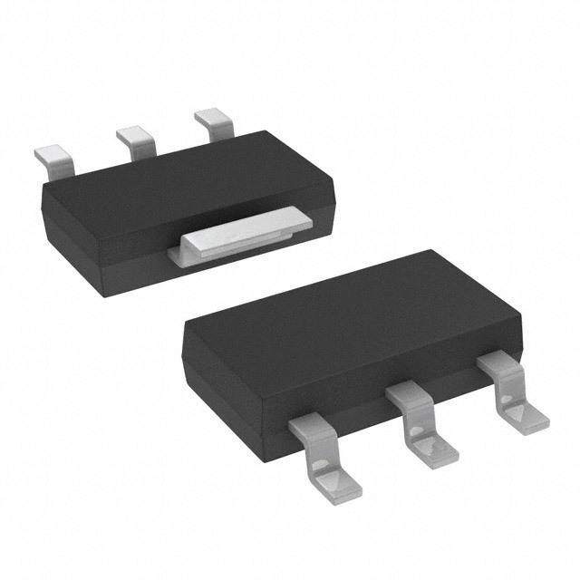
ICGOO电子元器件商城为您提供MMFT960T1G由ON Semiconductor设计生产,在icgoo商城现货销售,并且可以通过原厂、代理商等渠道进行代购。 MMFT960T1G价格参考。ON SemiconductorMMFT960T1G封装/规格:晶体管 - FET,MOSFET - 单, 表面贴装 N 沟道 60V 300mA(Tc) 800mW(Ta) SOT-223。您可以下载MMFT960T1G参考资料、Datasheet数据手册功能说明书,资料中有MMFT960T1G 详细功能的应用电路图电压和使用方法及教程。
| 参数 | 数值 |
| 产品目录 | |
| ChannelMode | Enhancement |
| 描述 | MOSFET N-CH 60V 300MA SOT223MOSFET 60V 300mA N-Channel |
| 产品分类 | FET - 单分离式半导体 |
| FET功能 | 逻辑电平门 |
| FET类型 | MOSFET N 通道,金属氧化物 |
| Id-ContinuousDrainCurrent | 300 mA |
| Id-连续漏极电流 | 300 mA |
| 品牌 | ON Semiconductor |
| 产品手册 | |
| 产品图片 |
|
| rohs | 符合RoHS无铅 / 符合限制有害物质指令(RoHS)规范要求 |
| 产品系列 | 晶体管,MOSFET,ON Semiconductor MMFT960T1G- |
| 数据手册 | |
| 产品型号 | MMFT960T1G |
| PCN设计/规格 | |
| Pd-PowerDissipation | 0.8 W |
| Pd-功率耗散 | 800 mW |
| RdsOn-Drain-SourceResistance | 1.7 Ohms |
| RdsOn-漏源导通电阻 | 1.7 Ohms |
| Vds-Drain-SourceBreakdownVoltage | 60 V |
| Vds-漏源极击穿电压 | 60 V |
| Vgs-Gate-SourceBreakdownVoltage | +/- 30 V |
| Vgs-栅源极击穿电压 | 30 V |
| 不同Id时的Vgs(th)(最大值) | 3.5V @ 1mA |
| 不同Vds时的输入电容(Ciss) | 65pF @ 25V |
| 不同Vgs时的栅极电荷(Qg) | 3.2nC @ 10V |
| 不同 Id、Vgs时的 RdsOn(最大值) | 1.7 欧姆 @ 1A,10V |
| 产品目录页面 | |
| 产品种类 | MOSFET |
| 供应商器件封装 | SOT-223 |
| 其它名称 | MMFT960T1GOSTR |
| 功率-最大值 | 800mW |
| 功率耗散 | 0.8 W |
| 包装 | 带卷 (TR) |
| 商标 | ON Semiconductor |
| 安装类型 | 表面贴装 |
| 安装风格 | SMD/SMT |
| 导通电阻 | 1.7 Ohms |
| 封装 | Reel |
| 封装/外壳 | TO-261-4,TO-261AA |
| 封装/箱体 | SOT-223-3 |
| 工厂包装数量 | 1000 |
| 晶体管极性 | N-Channel |
| 最大工作温度 | + 150 C |
| 最小工作温度 | - 65 C |
| 标准包装 | 1,000 |
| 正向跨导-最小值 | 0.6 S |
| 汲极/源极击穿电压 | 60 V |
| 漏极连续电流 | 300 mA |
| 漏源极电压(Vdss) | 60V |
| 电流-连续漏极(Id)(25°C时) | 300mA (Tc) |
| 系列 | MMFT960 |
| 通道模式 | Enhancement |
| 配置 | Single Dual Drain |
| 闸/源击穿电压 | +/- 30 V |


- 商务部:美国ITC正式对集成电路等产品启动337调查
- 曝三星4nm工艺存在良率问题 高通将骁龙8 Gen1或转产台积电
- 太阳诱电将投资9.5亿元在常州建新厂生产MLCC 预计2023年完工
- 英特尔发布欧洲新工厂建设计划 深化IDM 2.0 战略
- 台积电先进制程称霸业界 有大客户加持明年业绩稳了
- 达到5530亿美元!SIA预计今年全球半导体销售额将创下新高
- 英特尔拟将自动驾驶子公司Mobileye上市 估值或超500亿美元
- 三星加码芯片和SET,合并消费电子和移动部门,撤换高东真等 CEO
- 三星电子宣布重大人事变动 还合并消费电子和移动部门
- 海关总署:前11个月进口集成电路产品价值2.52万亿元 增长14.8%


PDF Datasheet 数据手册内容提取
MMFT960T1 Preferred Device Power MOSFET 300 mA, 60 Volts N−Channel SOT−223 This Power MOSFET is designed for high speed, low loss power http://onsemi.com switching applications such as switching regulators, dc−dc converters, solenoid and relay drivers. The device is housed in the SOT−223 300 mA, 60 VOLTS package which is designed for medium power surface mount R = 1.7 (cid:2) applications. DS(on) Features N−Channel • Silicon Gate for Fast Switching Speeds D • Low Drive Requirement • The SOT−223 Package can be Soldered Using Wave or Reflow • The Formed Leads Absorb Thermal Stress During Soldering G Eliminating the Possibility of Damage to the Die • Pb−Free Package is Available S MAXIMUM RATINGS (TC = 25°C unless otherwise noted) 4 Rating Symbol Value Unit TO−261AA CASE 318E Drain−to−Source Voltage VDS 60 V 1 2 STYLE 3 Gate−to−Source Voltage − Non−Repetitive VGS ±30 V 3 Drain Current ID 300 mAdc MARKING DIAGRAM AND Total Power Dissipation @ TA = 25°C PD 0.8 W PIN ASSIGNMENT (Note 1) Derate above 25°C 6.4 mW/°C 4 Drain Operating and Storage Temperature Range TJ, Tstg −65 to 150 °C AYW THERMAL CHARACTERISTICS FT960(cid:2) (cid:2) Thermal Resistance, Junction−to−Ambient R(cid:2)JA 156 °C/W Maximum Temperature for Soldering TL 260 °C 1 2 3 Purposes Gate Drain Source Time in Solder Bath 10 S A = Assembly Location Maximum ratings are those values beyond which device damage can occur. Y = Year Maximum ratings applied to the device are individual stress limit values (not W = Work Week normal operating conditions) and are not valid simultaneously. If these limits are (cid:2) = Pb−Free Package exceeded, device functional operation is not implied, damage may occur and reliability may be affected. FT960 = Device Code (Note: Microdot may be in either location) 1. Device mounted on a FR−4 glass epoxy printed circuit board using minimum recommended footprint. ORDERING INFORMATION Device Package Shipping† MMFT960T1 SOT−223 1000 Tape & Reel MMFT960T1G SOT−223 1000 Tape & Reel (Pb−Free) †For information on tape and reel specifications, including part orientation and tape sizes, please refer to our Tape and Reel Packaging Specifications Brochure, BRD8011/D. Preferred devices are recommended choices for future use and best overall value. © Semiconductor Components Industries, LLC, 2006 1 Publication Order Number: January, 2006 − Rev. 5 MMFT960T1/D
MMFT960T1 ELECTRICAL CHARACTERISTICS (TA = 25°C unless otherwise noted) Characteristic Symbol Min Typ Max Unit OFF CHARACTERISTICS Drain−to−Source Breakdown Voltage V(BR)DSS 60 − − Vdc (VGS = 0, ID = 10 (cid:3)A) Zero Gate Voltage Drain Current IDSS − − 10 (cid:3)Adc (VDS = 60 V, VGS = 0) Gate−Body Leakage Current IGSS − − 50 nAdc (VGS = 15 Vdc, VDS = 0) ON CHARACTERISTICS (Note 2) Gate Threshold Voltage VGS(th) 1.0 − 3.5 Vdc (VDS = VGS, ID = 1.0 mAdc) Static Drain−to−Source On−Resistance RDS(on) − − 1.7 (cid:4) (VGS = 10 Vdc, ID = 1.0 A) Drain−to−Source On−Voltage VDS(on) Vdc (VGS = 10 V, ID = 0.5 A) − − 0.8 (VGS = 10 V, ID = 1.0 A) − − 1.7 Forward Transconductance gfs − 600 − mmhos (VDS = 25 V, ID = 0.5 A) DYNAMIC CHARACTERISTICS Input Capacitance Ciss − 65 − pF Output Capacitance (VDS = 25 V, VGS = 0, f = 1.0 MHz) Coss − 33 − Transfer Capacitance Crss − 7.0 − Total Gate Charge Qg − 3.2 − nC Gate−Source Charge (VGS = 10 V, ID = 1.0 A, VDS = 48 V) Qgs − 1.2 − Gate−Drain Charge Qgd − 2.0 − 2. Pulse Test: Pulse Width ≤300 (cid:3)s, Duty Cycle ≤2.0%. TYPICAL ELECTRICAL CHARACTERISTICS 5 1 TJ = 25°C TJ = −(cid:2)55°C TJ = 25°C S) 4 S) 0.8 P P NT (AM 3 VGS = 10 V 8 V NT (AM 0.6 TJ = 125°C E E R R UR 7 V UR C C N 2 N 0.4 AI 6 V AI DR DR VDS = 10 V I, D 1 5 V I, D 0.2 4 V 0 0 0 2 4 6 8 10 0 2 4 6 8 10 VDS, DRAIN−TO−SOURCE VOLTAGE (VOLTS) VGS, GATE−TO−SOURCE VOLTAGE (VOLTS) Figure 1. On−Region Characteristics Figure 2. Transfer Characteristics http://onsemi.com 2
MMFT960T1 TYPICAL ELECTRICAL CHARACTERISTICS S) 5 ED) 10 M Z CE (OH 4 VGS = 10 V ORMALI IVDG =S 1= A10 V N N RESISTA 3 TANCE ( RCE TJ = 125°C ESIS 1 U R O 2 E S C AIN− 25°C OUR R S D 1 − , n) AIN o R S( −(cid:2)55°C D RD 0 , n) 0.1 0 0.5 1 1.5 2 2.5 S(o −(cid:2)75 −(cid:2)50 −(cid:2)25 0 25 50 75 100 125 150 ID, DRAIN CURRENT (AMPS) RD TJ, JUNCTION TEMPERATURE (°C) Figure 3. On−Resistance versus Drain Current Figure 4. On−Resistance Variation with Temperature 250 225 VGS = 0 V f = 1 MHz PS) 200 TJ = 25°C NT (AM 1 E (pF) 115705 E C R N N CUR TJ = 125°C TJ = 25°C PACITA 110205 I, DRAID 0.1 C, CA 5705 Coss Ciss 25 Crss 0 0 0.3 0.6 0.9 1.2 1.5 0 5 10 15 20 25 30 VSD, SOURCE−DRAIN DIODE FORWARD VOLTAGE (VOLTS) VDS, DRAIN−SOURCE VOLTAGE (VOLTS) Figure 5. Source−Drain Diode Forward Voltage Figure 6. Capacitance Variation S) 10 2 T OLTAGE (VOL 987 ITDJ == 12 5A°C VDS = 30 V NCE (mhos) 1.5 VDS = 10 V E V 6 VDS = 48 V CTA C U R 5 D 1 SOU 4 CON TJ = −(cid:2)55°C − S O N T 3 A , GATE−S 21 g, TRFS 0.5 125°C 25°C G V 0 0 0 0.5 1 1.5 2 2.5 3 3.5 4 0 0.5 1 1.5 2 2.5 Qg, TOTAL GATE CHARGE (nC) ID, DRAIN CURRENT (AMPS) Figure 7. Gate Charge versus Gate−to−Source Voltage Figure 8. Transconductance http://onsemi.com 3
MMFT960T1 PACKAGE DIMENSIONS SOT−223 (TO−261) CASE 318E−04 ISSUE L D NOTES: 1. DIMENSIONING AND TOLERANCING PER ANSI b1 Y14.5M, 1982. 2. CONTROLLING DIMENSION: INCH. 4 MILLIMETERS INCHES DIM MIN NOM MAX MIN NOM MAX HE E A 1.50 1.63 1.75 0.060 0.064 0.068 1 2 3 A1 0.02 0.06 0.10 0.001 0.002 0.004 b 0.60 0.75 0.89 0.024 0.030 0.035 b1 2.90 3.06 3.20 0.115 0.121 0.126 c 0.24 0.29 0.35 0.009 0.012 0.014 b D 6.30 6.50 6.70 0.249 0.256 0.263 E 3.30 3.50 3.70 0.130 0.138 0.145 e1 e 2.20 2.30 2.40 0.087 0.091 0.094 e e1 0.85 0.94 1.05 0.033 0.037 0.041 L1 1.50 1.75 2.00 0.060 0.069 0.078 (cid:3) C H(cid:3)E 60.7°0 7.−00 71.03°0 0.206°4 0.2−76 01.208°7 A STYLE 3: 0.08 (0003) PIN 1.GATE A1 2.DRAIN L1 3.SOURCE 4.DRAIN SOLDERING FOOTPRINT* 3.8 0.15 2.0 0.079 6.3 2.3 2.3 0.248 0.091 0.091 2.0 0.079 (cid:2) (cid:3) 1.5 mm SCALE 6:1 0.059 inches *For additional information on our Pb−Free strategy and soldering details, please download the ON Semiconductor Soldering and Mounting Techniques Reference Manual, SOLDERRM/D. ON Semiconductor and are registered trademarks of Semiconductor Components Industries, LLC (SCILLC). SCILLC reserves the right to make changes without further notice to any products herein. SCILLC makes no warranty, representation or guarantee regarding the suitability of its products for any particular purpose, nor does SCILLC assume any liability arising out of the application or use of any product or circuit, and specifically disclaims any and all liability, including without limitation special, consequential or incidental damages. “Typical” parameters which may be provided in SCILLC data sheets and/or specifications can and do vary in different applications and actual performance may vary over time. All operating parameters, including “Typicals” must be validated for each customer application by customer’s technical experts. SCILLC does not convey any license under its patent rights nor the rights of others. SCILLC products are not designed, intended, or authorized for use as components in systems intended for surgical implant into the body, or other applications intended to support or sustain life, or for any other application in which the failure of the SCILLC product could create a situation where personal injury or death may occur. Should Buyer purchase or use SCILLC products for any such unintended or unauthorized application, Buyer shall indemnify and hold SCILLC and its officers, employees, subsidiaries, affiliates, and distributors harmless against all claims, costs, damages, and expenses, and reasonable attorney fees arising out of, directly or indirectly, any claim of personal injury or death associated with such unintended or unauthorized use, even if such claim alleges that SCILLC was negligent regarding the design or manufacture of the part. SCILLC is an Equal Opportunity/Affirmative Action Employer. This literature is subject to all applicable copyright laws and is not for resale in any manner. PUBLICATION ORDERING INFORMATION LITERATURE FULFILLMENT: N. American Technical Support: 800−282−9855 Toll Free ON Semiconductor Website: http://onsemi.com Literature Distribution Center for ON Semiconductor USA/Canada P.O. Box 61312, Phoenix, Arizona 85082−1312 USA Order Literature: http://www.onsemi.com/litorder Phone: 480−829−7710 or 800−344−3860 Toll Free USA/Canada Japan: ON Semiconductor, Japan Customer Focus Center Fax: 480−829−7709 or 800−344−3867 Toll Free USA/Canada 2−9−1 Kamimeguro, Meguro−ku, Tokyo, Japan 153−0051 For additional information, please contact your Email: orderlit@onsemi.com Phone: 81−3−5773−3850 local Sales Representative. http://onsemi.com MMFT960T1/D 4