ICGOO在线商城 > 分立半导体产品 > 二极管 - 齐纳 - 单 > MMBZ5223BLT1G

 Datasheet下载
- 型号: MMBZ5223BLT1G
- 制造商: ON Semiconductor
- 库位|库存: xxxx|xxxx
- 要求:
| 数量阶梯 | 香港交货 | 国内含税 |
| +xxxx | $xxxx | ¥xxxx |
查看当月历史价格
查看今年历史价格
MMBZ5223BLT1G产品简介:
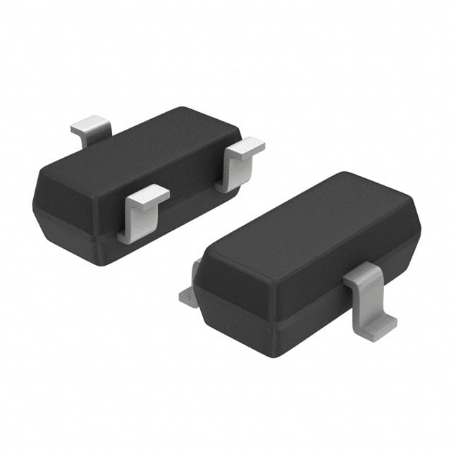
ICGOO电子元器件商城为您提供MMBZ5223BLT1G由ON Semiconductor设计生产,在icgoo商城现货销售,并且可以通过原厂、代理商等渠道进行代购。 MMBZ5223BLT1G价格参考。ON SemiconductorMMBZ5223BLT1G封装/规格:二极管 - 齐纳 - 单, Zener Diode 2.7V 225mW ±5% Surface Mount SOT-23-3 (TO-236)。您可以下载MMBZ5223BLT1G参考资料、Datasheet数据手册功能说明书,资料中有MMBZ5223BLT1G 详细功能的应用电路图电压和使用方法及教程。
| 参数 | 数值 |
| 产品目录 | |
| 描述 | DIODE ZENER 2.7V 225MW SOT23-3稳压二极管 2.7V 225mW |
| 产品分类 | 单二极管/齐纳分离式半导体 |
| 品牌 | ON Semiconductor |
| 产品手册 | |
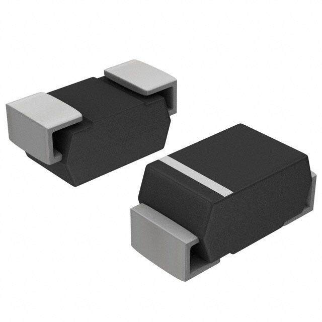
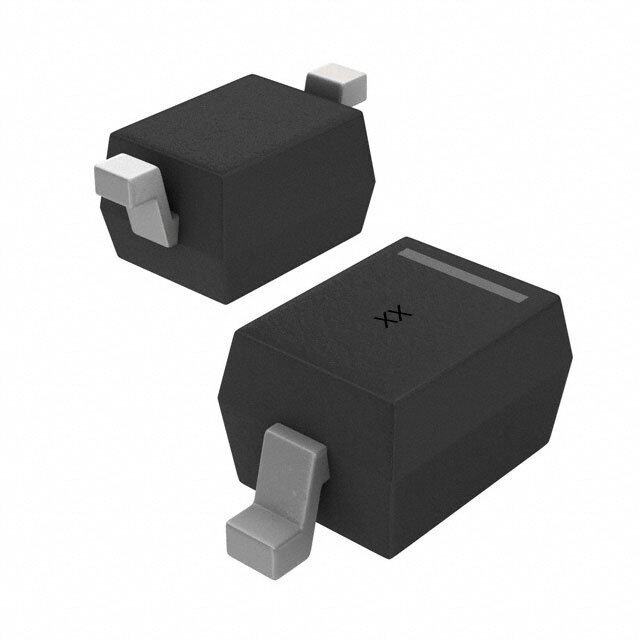
| 产品图片 |
|
| rohs | 符合RoHS无铅 / 符合限制有害物质指令(RoHS)规范要求 |
| 产品系列 | 二极管与整流器,稳压二极管,ON Semiconductor MMBZ5223BLT1G- |
| 数据手册 | |
| 产品型号 | MMBZ5223BLT1G |
| PCN设计/规格 | |
| 不同If时的电压-正向(Vf) | 900mV @ 10mA |
| 不同 Vr时的电流-反向漏电流 | 75µA @ 1V |
| 产品目录页面 | |
| 产品种类 | |
| 供应商器件封装 | SOT-23-3(TO-236) |
| 其它名称 | MMBZ5223BLT1GOSCT |
| 功率-最大值 | 225mW |
| 功率耗散 | 300 mW |
| 包装 | 剪切带 (CT) |
| 商标 | ON Semiconductor |
| 安装类型 | 表面贴装 |
| 安装风格 | SMD/SMT |
| 容差 | ±5% |
| 封装 | Reel |
| 封装/外壳 | TO-236-3,SC-59,SOT-23-3 |
| 封装/箱体 | SOT-23 |
| 工作温度 | -65°C ~ 150°C |
| 工厂包装数量 | 3000 |
| 最大反向漏泄电流 | 75 uA |
| 最大工作温度 | + 150 C |
| 最大齐纳阻抗 | 30 Ohms |
| 最小工作温度 | - 65 C |
| 标准包装 | 1 |
| 电压-齐纳(标称值)(Vz) | 2.7V |
| 电压容差 | 5 % |
| 系列 | MMBZ5223B |
| 配置 | Single |
| 阻抗(最大值)(Zzt) | 30 欧姆 |
| 齐纳电压 | 2.7 V |
| 齐纳电流 | 10 mA |


- 商务部:美国ITC正式对集成电路等产品启动337调查
- 曝三星4nm工艺存在良率问题 高通将骁龙8 Gen1或转产台积电
- 太阳诱电将投资9.5亿元在常州建新厂生产MLCC 预计2023年完工
- 英特尔发布欧洲新工厂建设计划 深化IDM 2.0 战略
- 台积电先进制程称霸业界 有大客户加持明年业绩稳了
- 达到5530亿美元!SIA预计今年全球半导体销售额将创下新高
- 英特尔拟将自动驾驶子公司Mobileye上市 估值或超500亿美元
- 三星加码芯片和SET,合并消费电子和移动部门,撤换高东真等 CEO
- 三星电子宣布重大人事变动 还合并消费电子和移动部门
- 海关总署:前11个月进口集成电路产品价值2.52万亿元 增长14.8%

PDF Datasheet 数据手册内容提取
MMBZ52xxBLT1G Series, SZMMBZ52xxBLT1G Series Zener Voltage Regulators 225 mW SOT−23 Surface Mount This series of Zener diodes is offered in the convenient, surface mount plastic SOT−23 package. These devices are designed to provide voltage regulation with minimum space requirement. They are well www.onsemi.com suited for applications such as cellular phones, hand held portables, and high density PC boards. Features • 225 mW Rating on FR−4 or FR−5 Board • Zener Voltage Range − 2.4 V to 91 V • SOT−23 Package Designed for Optimal Automated Board Assembly CASE 318 • Small Package Size for High Density Applications STYLE 8 • ESD Rating of Class 3 (>16 KV) per Human Body Model • SZ Prefix for Automotive and Other Applications Requiring Unique Site and Control Change Requirements; AEC−Q101 Qualified and 3 1 Cathode Anode PPAP Capable • These Devices are Pb−Free, Halogen Free/BFR Free and are RoHS MARKING DIAGRAM Compliant Mechanical Characteristics CASE: Void-free, transfer-molded, thermosetting plastic case xxxM (cid:2) (cid:2) FINISH: Corrosion resistant finish, easily solderable MAXIMUM CASE TEMPERATURE FOR SOLDERING PURPOSES: 260°C for 10 Seconds xxx = Specific Device Code POLARITY: Cathode indicated by polarity band M = Date Code FLAMMABILITY RATING: UL 94 V−0 (cid:2) = Pb−Free Package (Note: Microdot may be in either location) MAXIMUM RATINGS Rating Symbol Max Units ORDERING INFORMATION Total Power Dissipation on FR−5 Board, PD Device Package Shipping† (Note 1) @ TA = 25°C 225 mW Derated above 25°C 1.8 mW/°C MMBZ52xxBLT1G SOT−23 3,000 / (Pb−Free) Tape & Reel Thermal Resistance, R(cid:2)JA 556 °C/W Junction−to−Ambient SZMMBZ52xxBLT1G SOT−23 3,000 / (Pb−Free) Tape & Reel Total Power Dissipation on Alumina PD Substrate, (Note 2) @ TA = 25°C 300 mW MMBZ52xxBLT3G SOT−23 10,000 / Derated above 25°C 2.4 mW/°C (Pb−Free) Tape & Reel Thermal Resistance, R(cid:2)JA 417 °C/W SZMMBZ52xxBLT3G SOT−23 10,000 / Junction−to−Ambient (Pb−Free) Tape & Reel Junction and Storage TJ, Tstg −65 to +150 °C †Finocrlu indfionrgm paatriot no roienn ttaaptioen a anndd r etaepl esp seizceifsic,a ptiloenass,e Temperature Range refer to our Tape and Reel Packaging Specifications Stresses exceeding those listed in the Maximum Ratings table may damage the Brochure, BRD8011/D. device. If any of these limits are exceeded, device functionality should not be assumed, damage may occur and reliability may be affected. DEVICE MARKING INFORMATION 1. FR−5 = 1.0 X 0.75 X 0.62 in. 2. Alumina = 0.4 X 0.3 X 0.024 in, 99.5% alumina. See specific marking information in the device marking column of the Electrical Characteristics table on page 3 of this data sheet. © Semiconductor Components Industries, LLC, 2001 1 Publication Order Number: October, 2016 − Rev. 13 MMBZ5221BLT1/D
MMBZ52xxBLT1G Series, SZMMBZ52xxBLT1G Series ELECTRICAL CHARACTERISTICS (Pinout: 1-Anode, 2-No Connection, 3-Cathode) (TA = 25°C I unless otherwise noted, VF = 0.95 V Max. @ IF = 10 mA) IF Symbol Parameter VZ Reverse Zener Voltage @ IZT IZT Reverse Current ZZT Maximum Zener Impedance @ IZT VZ VR V IZK Reverse Current IIRZTVF ZZK Maximum Zener Impedance @ IZK IR Reverse Leakage Current @ VR VR Reverse Voltage IF Forward Current VF Forward Voltage @ IF Zener Voltage Regulator www.onsemi.com 2
MMBZ52xxBLT1G Series, SZMMBZ52xxBLT1G Series ELECTRICAL CHARACTERISTICS (Pinout: 1-Anode, 2-NC, 3-Cathode) (VF = 0.9 V Max @ IF = 10 mA for all types.) Zener Voltage (Note 3) Zener Impedance Leakage Current Device VZ (Volts) @ IZT ZZT @ IZT ZZK @ IZK IR @ VR Device* Marking Min Nom Max mA (cid:2) (cid:2) mA (cid:3)A Volts MMBZ5221BLT1G 18A 2.28 2.4 2.52 20 30 1200 0.25 100 1 MMBZ5222BLT1G 18B 2.37 2.5 2.63 20 30 1250 0.25 100 1 MMBZ5223BLT1G 18C 2.56 2.7 2.84 20 30 1300 0.25 75 1 MMBZ5224BLT1G 18D 2.66 2.8 2.94 20 30 1400 0.25 75 1 MMBZ5225BLT1G 18E 2.85 3 3.15 20 29 1600 0.25 50 1 MMBZ5226BLT1G 8A 3.13 3.3 3.47 20 28 1600 0.25 25 1 MMBZ5227BLT1G 8B 3.42 3.6 3.78 20 24 1700 0.25 15 1 MMBZ5228BLT1G 8C 3.70 3.9 4.10 20 23 1900 0.25 10 1 MMBZ5229BLT1G 8D 4.08 4.3 4.52 20 22 2000 0.25 5 1 MMBZ5230BLT1G 8E 4.46 4.7 4.94 20 19 1900 0.25 5 2 MMBZ5231BLT1G/T3G 8F 4.84 5.1 5.36 20 17 1600 0.25 5 2 MMBZ5232BLT1G/T3G 8G 5.32 5.6 5.88 20 11 1600 0.25 5 3 MMBZ5233BLT1G 8H 5.70 6 6.30 20 7 1600 0.25 5 3.5 MMBZ5234BLT1G/T3G 8J 5.89 6.2 6.51 20 7 1000 0.25 5 4 MMBZ5235BLT1G 8K 6.46 6.8 7.14 20 5 750 0.25 3 5 MMBZ5236BLT1G 8L 7.12 7.5 7.88 20 6 500 0.25 3 6 MMBZ5237BLT1G 8M 7.79 8.2 8.61 20 8 500 0.25 3 6.5 MMBZ5238BLT1G 8N 8.26 8.7 9.14 20 8 600 0.25 3 6.5 MMBZ5239BLT1G 8P 8.64 9.1 9.56 20 10 600 0.25 3 7 MMBZ5240BLT1G 8Q 9.50 10 10.50 20 17 600 0.25 3 8 MMBZ5241BLT1G/T3G 8R 10.4 11 11.55 20 22 600 0.25 2 8.4 MMBZ5242BLT1G/T3G 8S 11.40 12 12.60 20 30 600 0.25 1 9.1 MMBZ5243BLT1G 8T 12.35 13 13.65 9.5 13 600 0.25 0.5 9.9 MMBZ5244BLT1G 8U 13.30 14 14.70 9 15 600 0.25 0.1 10 MMBZ5245BLT1G 8V 14.25 15 15.75 8.5 16 600 0.25 0.1 11 MMBZ5246BLT1G 8W 15.20 16 16.80 7.8 17 600 0.25 0.1 12 MMBZ5247BLT1G/T3G 8X 16.15 17 17.85 7.4 19 600 0.25 0.1 13 MMBZ5248BLT1G/T3G 8Y 17.10 18 18.90 7 21 600 0.25 0.1 14 MMBZ5249BLT1G 8Z 18.05 19 19.95 6.6 23 600 0.25 0.1 14 MMBZ5250BLT1G/T3G 81A 19.00 20 21.00 6.2 25 600 0.25 0.1 15 MMBZ5251BLT1G 81B 20.90 22 23.10 5.6 29 600 0.25 0.1 17 MMBZ5252BLT1G 81C 22.80 24 25.20 5.2 33 600 0.25 0.1 18 MMBZ5253BLT1G 81D 23.75 25 26.25 5 35 600 0.25 0.1 19 MMBZ5254BLT1G 81E 25.65 27 28.35 4.6 41 600 0.25 0.1 21 MMBZ5255BLT1G 81F 26.60 28 29.40 4.5 44 600 0.25 0.1 21 MMBZ5256BLT1G 81G 28.50 30 31.50 4.2 49 600 0.25 0.1 23 MMBZ5257BLT1G/T3G 81H 31.35 33 34.65 3.8 58 700 0.25 0.1 25 MMBZ5258BLT1G 81J 34.20 36 37.80 3.4 70 700 0.25 0.1 27 MMBZ5259BLT1G 81K 37.05 39 40.95 3.2 80 800 0.25 0.1 30 MMBZ5260BLT1G 81L 40.85 43 45.15 3 93 900 0.25 0.1 33 MMBZ5261BLT1G/T3G 81M 44.65 47 49.35 2.7 105 1000 0.25 0.1 36 MMBZ5262BLT1G 81N 48.45 51 53.55 2.5 125 1100 0.25 0.1 39 MMBZ5263BLT1G 81P 53.20 56 58.80 2.2 150 1300 0.25 0.1 43 MMBZ5264BLT1G 81Q 57.00 60 63.00 2.1 170 1400 0.25 0.1 46 MMBZ5265BLT1G 81R 58.90 62 65.10 2 185 1400 0.25 0.1 47 MMBZ5266BLT1G 81S 64.60 68 71.40 1.8 230 1600 0.25 0.1 52 MMBZ5267BLT1G 81T 71.25 75 78.75 1.7 270 1700 0.25 0.1 56 MMBZ5268BLT1G 81U 77.90 82 86.10 1.5 330 2000 0.25 0.1 62 MMBZ5270BLT1G 81W 86.45 91 95.55 1.4 400 2300 0.25 0.1 69 Product parametric performance is indicated in the Electrical Characteristics for the listed test conditions, unless otherwise noted. Product performance may not be indicated by the Electrical Characteristics if operated under different conditions. 3. Zener voltage is measured with a pulse test current IZ at an ambient temperature of 25°C NOTE: MMBZ5233BLT1G, MMBZ5246BLT1G, MMBZ5251BLT1G, and MMBZ5252BLT1G Not Available in 10,000/Tape & Reel. *Include SZ-prefix devices where applicable. www.onsemi.com 3
MMBZ52xxBLT1G Series, SZMMBZ52xxBLT1G Series TYPICAL CHARACTERISTICS 8 100 C) °ENT (mV/ 567 TFOYPRI CMAMLB TZC5 2VxAxLBULETS1G SERIES °NT (mV/C) FTOYPRI CMAMLB TZC5 2VxAxLBULETS1G SERIES CI E OEFFI 34 VZ @ IZT EFFICI VZ @ IZT E C CO 10 R 2 E U R RAT 1 ATU MPE 0 PER E -1 M , TVZ-(cid:2)2 , TEZ θ V -(cid:2)3 θ 1 2 3 4 5 6 7 8 9 10 11 12 10 100 VZ, NOMINAL ZENER VOLTAGE (V) VZ, NOMINAL ZENER VOLTAGE (V) Figure 1. Temperature Coefficients Figure 2. Temperature Coefficients (Temperature Range −55°C to +150°C) (Temperature Range −55°C to +150°C) 1000 1000 TJ = 25°C 75 V (MMBZ5267BLT1G) ΩNCE ()100 IZ = 1 mA fIZ =(A 1C )k =H z0.1 IZ(DC) NT (mA)100 91 V (MMBZ5270BLT1G) MPEDA 5 mA CURRE C I D MI 20 mA AR A W DYN 10 OR 10 , ZT , FF Z I 150°C 75°C 25°C 0°C 1 1 1 10 100 0.4 0.5 0.6 0.7 0.8 0.9 1.0 1.1 1.2 VZ, NOMINAL ZENER VOLTAGE VF, FORWARD VOLTAGE (V) Figure 3. Effect of Zener Voltage on Figure 4. Typical Forward Voltage Zener Impedance www.onsemi.com 4
MMBZ52xxBLT1G Series, SZMMBZ52xxBLT1G Series TYPICAL CHARACTERISTICS 1000 1000 0 V BIAS TA = 25°C μA) 100 1 V BIAS T ( N 10 F) RE CE (p100 CUR 1 AN GE +150°C CIT BIAS AT KA 0.1 PA 50% OF VZ NOM EA A L 0.01 C, C 10 I, R0.001 +25°C −55°C 0.0001 1 0.00001 1 10 100 0 10 20 30 40 50 60 70 80 90 VZ, NOMINAL ZENER VOLTAGE (V) VZ, NOMINAL ZENER VOLTAGE (V) Figure 5. Typical Capacitance Figure 6. Typical Leakage Current 100 100 TA = 25°C TA = 25°C mA) 10 mA) 10 T ( T ( N N E E R R R R U 1 U 1 C C R R E E N N E E Z Z , Z 0.1 , Z0.1 I I 0.01 0.01 0 2 4 6 8 10 12 10 30 50 70 90 VZ, ZENER VOLTAGE (V) VZ, ZENER VOLTAGE (V) Figure 7. Zener Voltage versus Zener Current Figure 8. Zener Voltage versus Zener Current (V Up to 12 V) (12 V to 91 V) Z www.onsemi.com 5
MMBZ52xxBLT1G Series, SZMMBZ52xxBLT1G Series PACKAGE DIMENSIONS SOT−23 (TO−236) CASE 318−08 ISSUE AR D NOTES: 1. DIMENSIONING AND TOLERANCING PER ASME Y14.5M, 1994. 2. CONTROLLING DIMENSION: MILLIMETERS. 3. MAXIMUM LEAD THICKNESS INCLUDES LEAD FINISH. 0.25 MINIMUM LEAD THICKNESS IS THE MINIMUM THICKNESS OF 3 THE BASE MATERIAL. E HE T 4. DPRIMOETNRSUIOSINOSN DS, AONRD G EA DTEO BNUORTR INS.CLUDE MOLD FLASH, 1 2 MILLIMETERS INCHES DIM MIN NOM MAX MIN NOM MAX L A 0.89 1.00 1.11 0.035 0.039 0.044 3Xb L1 A1 0.01 0.06 0.10 0.000 0.002 0.004 b 0.37 0.44 0.50 0.015 0.017 0.020 e VIEW C c 0.08 0.14 0.20 0.003 0.006 0.008 TOP VIEW D 2.80 2.90 3.04 0.110 0.114 0.120 E 1.20 1.30 1.40 0.047 0.051 0.055 e 1.78 1.90 2.04 0.070 0.075 0.080 L 0.30 0.43 0.55 0.012 0.017 0.022 A L1 0.35 0.54 0.69 0.014 0.021 0.027 HE 2.10 2.40 2.64 0.083 0.094 0.104 T 0° −−− 10° 0° −−− 10° A1 c SIDE VIEW SEE VIEW C STYLE 8: END VIEW PIN 1. ANODE 2. NO CONNECTION 3. CATHODE RECOMMENDED SOLDERING FOOTPRINT* 3X 2.90 0.90 3X0.80 0.95 PITCH DIMENSIONS: MILLIMETERS *For additional information on our Pb−Free strategy and soldering details, please download the ON Semiconductor Soldering and Mounting Techniques Reference Manual, SOLDERRM/D. ON Semiconductor and are trademarks of Semiconductor Components Industries, LLC dba ON Semiconductor or its subsidiaries in the United States and/or other countries. ON Semiconductor owns the rights to a number of patents, trademarks, copyrights, trade secrets, and other intellectual property. A listing of ON Semiconductor’s product/patent coverage may be accessed at www.onsemi.com/site/pdf/Patent−Marking.pdf. ON Semiconductor reserves the right to make changes without further notice to any products herein. ON Semiconductor makes no warranty, representation or guarantee regarding the suitability of its products for any particular purpose, nor does ON Semiconductor assume any liability arising out of the application or use of any product or circuit, and specifically disclaims any and all liability, including without limitation special, consequential or incidental damages. Buyer is responsible for its products and applications using ON Semiconductor products, including compliance with all laws, regulations and safety requirements or standards, regardless of any support or applications information provided by ON Semiconductor. “Typical” parameters which may be provided in ON Semiconductor data sheets and/or specifications can and do vary in different applications and actual performance may vary over time. All operating parameters, including “Typicals” must be validated for each customer application by customer’s technical experts. ON Semiconductor does not convey any license under its patent rights nor the rights of others. ON Semiconductor products are not designed, intended, or authorized for use as a critical component in life support systems or any FDA Class 3 medical devices or medical devices with a same or similar classification in a foreign jurisdiction or any devices intended for implantation in the human body. Should Buyer purchase or use ON Semiconductor products for any such unintended or unauthorized application, Buyer shall indemnify and hold ON Semiconductor and its officers, employees, subsidiaries, affiliates, and distributors harmless against all claims, costs, damages, and expenses, and reasonable attorney fees arising out of, directly or indirectly, any claim of personal injury or death associated with such unintended or unauthorized use, even if such claim alleges that ON Semiconductor was negligent regarding the design or manufacture of the part. ON Semiconductor is an Equal Opportunity/Affirmative Action Employer. This literature is subject to all applicable copyright laws and is not for resale in any manner. PUBLICATION ORDERING INFORMATION LITERATURE FULFILLMENT: N. American Technical Support: 800−282−9855 Toll Free ON Semiconductor Website: www.onsemi.com Literature Distribution Center for ON Semiconductor USA/Canada 19521 E. 32nd Pkwy, Aurora, Colorado 80011 USA Europe, Middle East and Africa Technical Support: Order Literature: http://www.onsemi.com/orderlit Phone: 303−675−2175 or 800−344−3860 Toll Free USA/Canada Phone: 421 33 790 2910 Fax: 303−675−2176 or 800−344−3867 Toll Free USA/Canada Japan Customer Focus Center For additional information, please contact your local Email: orderlit@onsemi.com Phone: 81−3−5817−1050 Sales Representative ◊ www.onsemi.com MMBZ5221BLT1/D 6
Mouser Electronics Authorized Distributor Click to View Pricing, Inventory, Delivery & Lifecycle Information: O N Semiconductor: MMBZ5221BLT1G MMBZ5222BLT1G MMBZ5223BLT1G MMBZ5225BLT1G MMBZ5226BLT1G MMBZ5227BLT1G MMBZ5229BLT1G MMBZ5230BLT1G MMBZ5231BLT3G MMBZ5232BLT1G MMBZ5233BLT1G MMBZ5234BLT1G MMBZ5235BLT1G MMBZ5236BLT1G MMBZ5237BLT1G MMBZ5238BLT1G MMBZ5239BLT1G MMBZ5240BLT1G MMBZ5241BLT1G MMBZ5242BLT1G MMBZ5243BLT1G MMBZ5244BLT1G MMBZ5245BLT1G MMBZ5246BLT1G MMBZ5247BLT1G MMBZ5248BLT1G MMBZ5248BLT3G MMBZ5249BLT1G MMBZ5250BLT1G MMBZ5251BLT1G MMBZ5252BLT1G MMBZ5254BLT1G MMBZ5255BLT1G MMBZ5256BLT1G MMBZ5257BLT1G MMBZ5258BLT1G MMBZ5259BLT1G MMBZ5260BLT1G MMBZ5261BLT1G MMBZ5263BLT1G MMBZ5264BLT1G MMBZ5268BLT1G MMBZ5270BLT1G MMBZ5242BLT3G SMBZ1443LT3DSG