ICGOO在线商城 > 分立半导体产品 > 晶体管 - 双极 (BJT) - 单 > MMBTA14
 Datasheet下载
- 型号: MMBTA14
- 制造商: Fairchild Semiconductor
- 库位|库存: xxxx|xxxx
- 要求:
| 数量阶梯 | 香港交货 | 国内含税 |
| +xxxx | $xxxx | ¥xxxx |
查看当月历史价格
查看今年历史价格
MMBTA14产品简介:
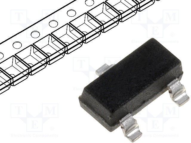
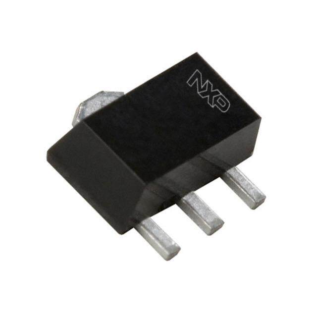
ICGOO电子元器件商城为您提供MMBTA14由Fairchild Semiconductor设计生产,在icgoo商城现货销售,并且可以通过原厂、代理商等渠道进行代购。 MMBTA14价格参考¥0.14-¥0.14。Fairchild SemiconductorMMBTA14封装/规格:晶体管 - 双极 (BJT) - 单, 双极 (BJT) 晶体管 NPN - 达林顿 30V 1.2A 125MHz 350mW 表面贴装 SOT-23-3。您可以下载MMBTA14参考资料、Datasheet数据手册功能说明书,资料中有MMBTA14 详细功能的应用电路图电压和使用方法及教程。
| 参数 | 数值 |
| 产品目录 | |
| 描述 | TRANS NPN GP 30V 1.2A SOT-23达林顿晶体管 NPN Transistor Darlington |
| 产品分类 | 晶体管(BJT) - 单路分离式半导体 |
| 品牌 | Fairchild Semiconductor |
| 产品手册 | |
| 产品图片 |
|
| rohs | 符合RoHS无铅 / 符合限制有害物质指令(RoHS)规范要求 |
| 产品系列 | 晶体管,达林顿晶体管,Fairchild Semiconductor MMBTA14- |
| 数据手册 | |
| 产品型号 | MMBTA14 |
| PCN封装 | |
| PCN组件/产地 | |
| PCN设计/规格 | |
| 不同 Ib、Ic时的 Vce饱和值(最大值) | 1.5V @ 100µA, 100mA |
| 不同 Ic、Vce 时的DC电流增益(hFE)(最小值) | 20000 @ 100mA,5V |
| 产品种类 | |
| 供应商器件封装 | SOT-23-3 |
| 其它名称 | MMBTA14FSCT |
| 功率-最大值 | 350mW |
| 包装 | 剪切带 (CT) |
| 单位重量 | 60 mg |
| 发射极-基极电压VEBO | 10 V |
| 商标 | Fairchild Semiconductor |
| 安装类型 | 表面贴装 |
| 安装风格 | SMD/SMT |
| 封装 | Reel |
| 封装/外壳 | TO-236-3,SC-59,SOT-23-3 |
| 封装/箱体 | SOT-23 |
| 工厂包装数量 | 3000 |
| 晶体管极性 | NPN |
| 晶体管类型 | NPN - 达林顿 |
| 最大工作温度 | + 150 C |
| 最大直流电集电极电流 | 1.2 A |
| 最大集电极截止电流 | 0.1 uA |
| 最小工作温度 | - 55 C |
| 标准包装 | 1 |
| 电压-集射极击穿(最大值) | 30V |
| 电流-集电极(Ic)(最大值) | 1.2A |
| 电流-集电极截止(最大值) | - |
| 直流集电极/BaseGainhfeMin | 10000 |
| 系列 | MMBTA14 |
| 配置 | Single |
| 集电极—发射极最大电压VCEO | 30 V |
| 集电极—基极电压VCBO | 30 V |
| 零件号别名 | MMBTA14_NL |
| 频率-跃迁 | 125MHz |


- 商务部:美国ITC正式对集成电路等产品启动337调查
- 曝三星4nm工艺存在良率问题 高通将骁龙8 Gen1或转产台积电
- 太阳诱电将投资9.5亿元在常州建新厂生产MLCC 预计2023年完工
- 英特尔发布欧洲新工厂建设计划 深化IDM 2.0 战略
- 台积电先进制程称霸业界 有大客户加持明年业绩稳了
- 达到5530亿美元!SIA预计今年全球半导体销售额将创下新高
- 英特尔拟将自动驾驶子公司Mobileye上市 估值或超500亿美元
- 三星加码芯片和SET,合并消费电子和移动部门,撤换高东真等 CEO
- 三星电子宣布重大人事变动 还合并消费电子和移动部门
- 海关总署:前11个月进口集成电路产品价值2.52万亿元 增长14.8%


PDF Datasheet 数据手册内容提取
Is Now Part of To learn more about ON Semiconductor, please visit our website at www.onsemi.com Please note: As part of the Fairchild Semiconductor integration, some of the Fairchild orderable part numbers will need to change in order to meet ON Semiconductor’s system requirements. Since the ON Semiconductor product management systems do not have the ability to manage part nomenclature that utilizes an underscore (_), the underscore (_) in the Fairchild part numbers will be changed to a dash (-). This document may contain device numbers with an underscore (_). Please check the ON Semiconductor website to verify the updated device numbers. The most current and up-to-date ordering information can be found at www.onsemi.com. Please email any questions regarding the system integration to Fairchild_questions@onsemi.com. ON Semiconductor and the ON Semiconductor logo are trademarks of Semiconductor Components Industries, LLC dba ON Semiconductor or its subsidiaries in the United States and/or other countries. ON Semiconductor owns the rights to a number of patents, trademarks, copyrights, trade secrets, and other intellectual property. A listing of ON Semiconductor’s product/patent coverage may be accessed at www.onsemi.com/site/pdf/Patent-Marking.pdf. ON Semiconductor reserves the right to make changes without further notice to any products herein. ON Semiconductor makes no warranty, representation or guarantee regarding the suitability of its products for any particular purpose, nor does ON Semiconductor assume any liability arising out of the application or use of any product or circuit, and specifically disclaims any and all liability, including without limitation special, consequential or incidental damages. Buyer is responsible for its products and applications using ON Semiconductor products, including compliance with all laws, regulations and safety requirements or standards, regardless of any support or applications information provided by ON Semiconductor. “Typical” parameters which may be provided in ON Semiconductor data sheets and/or specifications can and do vary in different applications and actual performance may vary over time. All operating parameters, including “Typicals” must be validated for each customer application by customer’s technical experts. ON Semiconductor does not convey any license under its patent rights nor the rights of others. ON Semiconductor products are not designed, intended, or authorized for use as a critical component in life support systems or any FDA Class 3 medical devices or medical devices with a same or similar classification in a foreign jurisdiction or any devices intended for implantation in the human body. Should Buyer purchase or use ON Semiconductor products for any such unintended or unauthorized application, Buyer shall indemnify and hold ON Semiconductor and its officers, employees, subsidiaries, affiliates, and distributors harmless against all claims, costs, damages, and expenses, and reasonable attorney fees arising out of, directly or indirectly, any claim of personal injury or death associated with such unintended or unauthorized use, even if such claim alleges that ON Semiconductor was negligent regarding the design or manufacture of the part. ON Semiconductor is an Equal Opportunity/Affirmative Action Employer. This literature is subject to all applicable copyright laws and is not for resale in any manner.
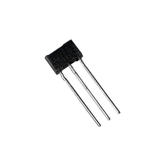
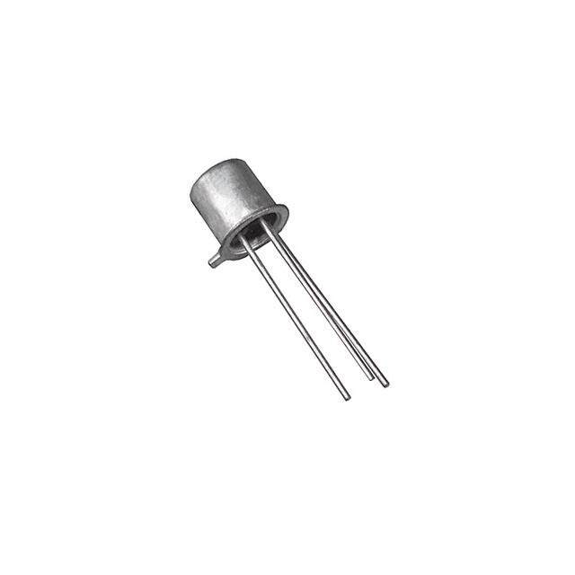
M P S A 1 4 / M M MPSA14 MMBTA14 PZTA14 B T A 1 4 C C / P Z E E T C A C TO-92 B 1 BE SOT-23 B SOT-223 4 Mark: 1N NPN Darlington Transistor This device is designed for applications requiring extremely high current gain at collector currents to 1.0 A. Sourced from Process 05. Absolute Maximum Ratings* TA = 25°C unless otherwise noted Symbol Parameter Value Units V Collector-Emitter Voltage 30 V CES V Collector-Base Voltage 30 V CBO V Emitter-Base Voltage 10 V EBO I Collector Current - Continuous 1.2 A C TJ, Tstg Operating and Storage Junction Temperature Range -55 to +150 °C * These ratings are limiting values above which the serviceability of any semiconductor device may be impaired. NOTES: 1) These ratings are based on a maximum junction temperature of 150 degrees C. 2) These are steady state limits. The factory should be consulted on applications involving pulsed or low duty cycle operations. Thermal Characteristics TA = 25°C unless otherwise noted Symbol Characteristic Max Units MPSA14 *MMBTA14 **PZTA14 P Total Device Dissipation 625 350 1,000 mW D Derate above 25°C 5.0 2.8 8.0 mW/°C RθJC Thermal Resistance, Junction to Case 83.3 °C/W RθJA Thermal Resistance, Junction to Ambient 200 357 125 °C/W * Device mounted on FR-4 PCB 1.6" X 1.6" X 0.06." **Device mounted on FR-4 PCB 36 mm X 18 mm X 1.5 mm; mounting pad for the collector lead min. 6 cm2. 1997 Fairchild Semiconductor Corporation A14, Rev B
M NPN Darlington Transistor P (continued) S A Electrical Characteristics 1 TA = 25°C unless otherwise noted 4 Symbol Parameter Test Conditions Min Max Units / M M OFF CHARACTERISTICS B V Collector-Emitter Breakdown Voltage I = 100 µA, I = 0 30 V T (BR)CES C B A I Collector-Cutoff Current V = 30 V, I = 0 100 nA CBO CB E 1 I Emitter-Cutoff Current V = 10 V, I = 0 100 nA 4 EBO EB C / P ON CHARACTERISTICS* Z hFE DC Current Gain IC = 10 mA, VCE = 5.0 V 10,000 T I = 100 mA, V = 5.0 V 20,000 A C CE VCE(sat) Collector-Emitter Saturation Voltage IC = 100 mA, IB = 0.1 mA 1.5 V 14 VBE(on) Base-Emitter On Voltage IC = 100 mA, VCE = 5.0 V 2.0 V SMALL SIGNAL CHARACTERISTICS fT Current Gain - Bandwidth Product IC = 10 mA, VCE = 5 V, 125 MHz f = 100 MHz *Pulse Test: Pulse Width ≤ 300 µs, Duty Cycle ≤ 2.0% Typical Characteristics Typical Pulsed Current Gain Collector-Emitter Saturation RENT GAIN (K)220500 V C E = 5vVs Collector Cu1r2r5e °Cnt R VOLTAGE (V)11..26 Vβo= l1ta00g0e vs Collector Current R E PULSED CU110500 25 °C CTOR EMITT0.8 - 40 °C 25°C 125 °C L - 40 °C E0.4 A 50 L C L h - TYPIFE 00.001 I C - CO0.0LL1ECTOR CURR0E.1NT (A) 1 V - COCESAT 01 I C - COL1L0ECTOR CURRE10N0T (mA) 1000 Base-Emitter Saturation Base Emitter ON Voltage vs Voltage vs Collector Current Collector Current TTER VOLTAGE (V)11..262 β = 1 -0 4000 °C 25 °C 125 °C ER ON VOLTAGE (V)11..262 - 40 °C 25 °C 125 °C ASE EMI0.8 E EMITT0.8 V = 5V V - BBESAT0.401 I C - COL1L0ECTOR CURRE10N0T (mA) 1000 V - BASBEON0.401 I C - COL1L0ECTOR CURRE10N0T (CmE A) 1000
M NPN Darlington Transistor P (continued) S A 1 4 Typical Characteristics (continued) / M M Collector-Emitter Breakdown Collector-Cutoff Current B Voltage with Resistance T vs Ambient Temperature A Between Emitter-Base A) 100 V) 1 T (n VC B = 30V GE (62.5 4 RREN 10 OLTA 62 / P LECTOR CU 1 AKDOWN V66016..155 TA1Z OL 0.1 RE 4 I - CCBO0.0125 50 75 100 125 BV - BCER596.050.1 1 10 100 1000 T - AMBIENT TEMPERATURE ( ° C) RESISTANCE (k Ω ) A Input and Output Capacitance Gain Bandwidth Product vs Collector Current vs Reverse Voltage z) MH500 f = 1.0 MHz T ( V c e = 5V 20 C F) DU400 NCE (p 10 H PRO300 TA Cib DT CI WI200 A 5 D P N A Cob A C N B100 AI 2 G 0.1 V - CO1LLECTOR VOLT1A0GE(V) 100 f - T 01 I - COLLECTO10R CU2R0RENT (5m0A) 100 150 C Power Dissipation vs Ambient Temperature 1 W) N ( SOT-223 O0.75 TI TO-92 A P SI DIS 0.5 R SOT-23 E W PO0.25 P - D 0 0 25 50 75 100 125 150 TEMPERATURE ( o C)
TO-92 Tape and Reel Data TO-92 Packaging Configuration: Figure 1.0 TAPE and REEL OPTION FSCINT Label sample See Fig 2.0 for various FAIRCHILD SEMICONDUCTOR CORPORATION HTB:B Reeling Styles LOT: CBVK741B019 QTY: 10000 NSID: PN2222N SPEC: FSCINT Label D/C1: D 9842 SPEC REV: B2 QA REV: 5 Reels per (FSCINT) Intermediate Box Customized F63TNR Label sample Label LOT: CBVK741B019 QTY: 2000 F63TNR Label FSID: PN222N SPEC: Customized DD//CC12:: D9842 QQTTYY12:: SCPPENC: REVN:/ F : F ( F63TNR)3 Label 375mm x 267mm x 375mm Intermediate Box TO-92 TNR/AMMO PACKING INFROMATION AMMO PACK OPTION See Fig 3.0 for 2 Ammo Packing Style Quantity EOL code Pack Options Reel A 2,000 D26Z E 2,000 D27Z Ammo M 2,000 D74Z P 2,000 D75Z FSCINT Unit weight = 0.22 gm Reel weight with components = 1.04 kg Label Ammo weight with components = 1.02 kg Max quantity per intermediate box = 10,000 units 327mm x 158mm x 135mm 5 Ammo boxes per Immediate Box Intermediate Box Customized Label Customized F63TNR Label Label 333mm x 231mm x 183mm Intermediate Box (TO-92) BULK PACKING INFORMATION BULK OPTION CEOODLE DESCRIPTION DLIEMAEDNCSLIOIPN QUANTITY SInefeo rBmualkti oPna ctakbinleg J18Z TO-18 OPTION STD NO LEAD CLIP 2.0 K / BOX Anti-static J05Z TO-5 OPTION STD NO LEAD CLIP 1.5 K / BOX FSCINT Label Bubble Sheets NCOO EDOEL TSOTR-9A2I G SHTTA NFODRAR: PDKG 92, NO LEADCLIP 2.0 K / BOX 94 (NON PROELECTRON SERIES), 96 L34Z TSOTR-9A2I G SHTTA NFODRAR: PDKG 94 NO LEADCLIP 2.0 K / BOX (PROELECTRON SERIES 2000 units per 114mm x 102mm x 51mm 9B7C, X9X8X, BFXXX, BSRXXX), EOs7td0 o bpotixo nfor Immediate Box 5 EO70 boxes per intermediate Box 530mm x 130mm x83mm Customized Intermediate box Label FSCINT Label 10,000 units maximum perintermediate box for std option ©2001 Fairchild Semiconductor Corporation March 2001, Rev. B1
TO-92 Tape and Reel Data, continued TO-92 Reeling Style Configuration: Figure 2.0 Machine Option “A” (H) Machine Option “E” (J) Style “A”, D26Z, D70Z (s/h) Style “E”, D27Z, D71Z (s/h) TO-92 Radial Ammo Packaging Configuration: Figure 3.0 FIRST WIRE OFF IS COLLECTOR FIRST WIRE OFF IS EMITTER ADHESIVE TAPE IS ON THE TOP SIDE ADHESIVE TAPE IS ON THE TOP SIDE FLAT OF TRANSISTOR IS ON TOP FLAT OF TRANSISTOR IS ON BOTTOM ORDER STYLE ORDER STYLE D74Z (M) D75Z (P) FAIDRHSETS WIVIER ET AOPF EF IISS OENM IBTOTETRTO (OMN S PIDKEG. 92) FAIDRHSETS WIVIER ET AOPFEF IISS OCNO LBLOETCTTOOMR S(OIDNE PKG. 92) FLAT OF TRANSISTOR IS ON BOTTOM FLAT OF TRANSISTOR IS ON TOP September 1999, Rev. B
TO-92 Tape and Reel Data, continued TO-92 Tape and Reel Taping Dimension Configuration: Figure 4.0 Hd P Pd b Ha W1 d S L H1 HO L1 WO t W2 W t1 P1 F1 P2 DO ITEM DESCRIPTION SYMBOL DIMENSION PO Base of Package to Lead Bend b 0.098 (max) User Direction of Feed Component Height Ha 0.928 (+/- 0.025) Lead Clinch Height HO 0.630 (+/- 0.020) Component Base Height H1 0.748 (+/- 0.020) Component Alignment ( side/side ) Pd 0.040 (max) Component Alignment ( front/back ) Hd 0.031 (max) Component Pitch P 0.500 (+/- 0.020) Feed Hole Pitch PO 0.500 (+/- 0.008) Hole Center to First Lead P1 0.150 (+0.009, -0.010) Hole Center to Component Center P2 0.247 (+/- 0.007) Lead Spread F1/F2 0.104 (+/- 0 .010) Lead Thickness d 0.018 (+0.002, -0.003) Cut Lead Length L 0.429 (max) Taped Lead Length L1 0.209 (+0.051, -0.052) Taped Lead Thickness t 0.032 (+/- 0.006) Carrier Tape Thickness t1 0.021 (+/- 0.006) Carrier Tape Width W 0.708 (+0.020, -0.019) TO-92 Reel Hold - down Tape Width WO 0.236 (+/- 0.012) Configuration: Figure 5.0 Hold - down Tape position W1 0.035 (max) Feed Hole Position W2 0.360 (+/- 0.025) Sprocket Hole Diameter DO 0.157 (+0.008, -0.007) Lead Spring Out S 0.004 (max) Note : All dimensions are in inches. ELECTROSTATIC SENSITIVE DEVICES D4 D1 ITEM DESCRIPTION SYSMBOL MINIMUM MAXIMUM F63TNR Label D2 Reel Diameter D1 13.975 14.025 Arbor Hole Diameter (Standard) D2 1.160 1.200 Customized Label (Small Hole) D2 0.650 0.700 Core Diameter D3 3.100 3.300 Hub Recess Inner Diameter D4 2.700 3.100 Hub Recess Depth W1 0.370 0.570 Flange to Flange Inner Width W2 1.630 1.690 W1 Hub to Hub Center Width W3 2.090 W2 W3 Note: All dimensions are inches D3 July 1999, Rev. A
TO-92 Package Dimensions TO-92 (FS PKG Code 92, 94, 96) 1:1 Scale 1:1 on letter size paper Dimensions shown below are in: inches [millimeters] Part Weight per unit (gram): 0.1977 ©2000 Fairchild Semiconductor International January 2000, Rev. B
SOT-23 Tape and Reel Data SOT-23 Packaging Configuration: Figure 1.0 Customized Label Packaging Description: SOT-23parts are shipped in tape. The carrier tape is made from a dissipative (carbon filled) polycarbonate resin. The cover tape is a multilayer film (Heat Activated Adhesive in nature) primarily composed of polyester film, adhesive layer, sealant, and anti-static sprayed agent. Antistatic Cover Tape These reeled parts in standard option are shipped with 3,000 units per 7" or 177cm diameter reel. The reels are dark blue in color and is made of polystyrene plastic (anti- static coated). Other option comes in 10,000 units per 13" or 330cm diameter reel. This and some other options are described in the Packaging Information table. These full reels are individually labeled and placed inside a standard intermediate made of recyclable corrugated brown paper with a Fairchild logo printing. One pizza box contains eight reels maximum. And these intermediate boxes are placed inside a labeled shipping box which comes in different sizes depending on the number of parts Human Readable Embossed shipped. Label Carrier Tape 3P 3P 3P 3P SOT-23 Packaging Information Packaging Option (noS ftlaonwd acrodde) D87Z SOT-23 Unit Or ientation Packaging type TNR TNR Qty per Reel/Tube/Bag 3,000 10,000 Reel Size 7" Dia 13" Box Dimension (mm) 187x107x183 343x343x64 343mm x 342mm x 64mm Human Readable Label Max qty per Box 24,000 30,000 Intermediate box for L87Z Option Weight per unit (gm) 0.0082 0.0082 Weight per Reel (kg) 0.1175 0.4006 Note/Comments Human Readable Label sample Human readable Label 187mm x 107mm x 183mm SOT-23 Tape Leader and Trailer Intermediate Box for Standard Option Configuration: Figure 2.0 Carrier Tape Components Cover Tape Trailer Tape Leader Tape 300mm minimum or 500mm minimum or 75 empty pockets 125 empty pockets ©2000 Fairchild Semiconductor International September 1999, Rev. C
SOT-23 Tape and Reel Data, continued SOT-23 Embossed Carrier Tape Configuration: Figure 3.0 P0 P2 D0 D1 T E1 F W E2 B0 Wc Tc P1 A0 K0 User Direction of Feed Dimensions are in millimeter Pkg type A0 B0 W D0 D1 E1 E2 F P1 P0 K0 T Wc Tc SOT-23 3.15 2.77 8.0 1.55 1.125 1.75 6.25 3.50 4.0 4.0 1.30 0.228 5.2 0.06 (8mm) +/-0.10 +/-0.10 +/-0.3 +/-0.05 +/-0.125 +/-0.10 min +/-0.05 +/-0.1 +/-0.1 +/-0.10 +/-0.013 +/-0.3 +/-0.02 Notes: A0, B0, and K0 dimensions are determined with respect to the EIA/Jedec RS-481 rotational and lateral movement requirements (see sketches A, B, and C). 0.5mm 20 deg maximum maximum Typical component cavity 0.5mm B0 center line maximum 20 deg maximum component rotation Typical Sketch A (Side or Front Sectional View) component Sketch C (Top View) Component Rotation A0 center line Component lateral movement Sketch B (Top View) SOT-23 Reel Configuration: Figure 4.0 Component Rotation W1 Measured at Hub Dim A Max Dim A See detail AA max Dim N 7" Diameter Option B Min Dim C See detail AA Dim D W3 min 13" Diameter Option W2 max Measured at Hub DETAIL AA Dimensions are in inches and millimeters Reel Tape Size Dim A Dim B Dim C Dim D Dim N Dim W1 Dim W2 Dim W3 (LSL-USL) Option 8mm 7" Dia 71.7070.8 01..0559 51132 + +00.5.0/-200.2/-0.008 02.07.925 25.5165 08..343 +11 +.50/0.059/-0.000 01.45.647 07..391 –1 1 –0 0.9.429 8mm 13" Dia 1333.000 01..0559 51132 + +00.5.0/-200.2/-0.008 02.07.925 41.0000 08..343 +11 +.50/0.059/-0.000 01.45.647 07..391 –1 1 –0 0.9.429 September 1999, Rev. C
SOT-23 Package Dimensions SOT-23 (FS PKG Code 49) 1:1 Scale 1:1 on letter size paper Dimensions shown below are in: inches [millimeters] Part Weight per unit (gram): 0.0082 ©2000 Fairchild Semiconductor International September 1998, Rev. A1
SOT-223 Tape and Reel Data SOT-223 Packaging Configuration: Figure 1.0 Customized Label Packaging Description: SOT-223 parts are shipped in tape. The carrier tape is made from a dissipative (carbon filled) polycarbonate F63TNR Label resin. The cover tape is a multilayer film (Heat Activated Adhesive in nature) primarily composed of polyester film, Antistatic Cover Tape aTdhheessei vree ellaeyde rp, asrtesa liann st,t aanndda rda notip-stitoanti ca rsep rsahyieppd eda gwenitth. 2,500 units per 13" or 330cm diameter reel. The reels are dark blue in color and is made of polystyrene plastic (anti- static coated). Other option comes in 500 units per 7" or 177cm diameter reel. This and some other options are further described in the Packaging Information table. These full reels are individually barcode labeled and placed inside a standard intermediate box (illustrated in figure 1.0) made of recyclable corrugated brown paper. One box contains two reels maximum. And these boxes are placed inside a barcode labeled shipping box which Static Dissipative comes in different sizes depending on the number of parts Embossed Carrier Tape shipped. F852 F852 F852 F852 014 014 014 014 SOT-223 Packaging Information Packaging Option (noS ftlaonwd acordde) D84Z SOT-223 Unit Orientation Packaging type TNR TNR Qty per Reel/Tube/Bag 2,500 500 Reel Size 13" Dia 7" Dia Box Dimension (mm) 343x64x343 184x187x47 Max qty per Box 5,000 1,000 343mm x 342mm x 64mm Weight per unit (gm) 0.1246 0.1246 Intermediate box for Standard F63TNR Label Weight per Reel (kg) 0.7250 0.1532 Note/Comments F63TNR Label F63TNR Label sample 184mm x 184mm x 47mm Pizza Box for D84Z Option LOT: CBVK741B019 QTY: 3000 FSID: PN2222A SPEC: SOT-223 Tape Leader and Trailer Configuration: Figure 2.0 D/C1: D9842 QTY1: SPEC REV: D/C2: QTY2: CPN: N/F: F (F63TNR)3 Carrier Tape Components Cover Tape Trailer Tape Leader Tape 300mm minimum or 500mm minimum or 38 empty pockets 62 empty pockets ©2000 Fairchild Semiconductor International September 1999, Rev. B
SOT-223 Tape and Reel Data, continued SOT-223 Embossed Carrier Tape Configuration: Figure 3.0 P0 D0 T E1 F K0 E2 W Wc B0 Tc A0 P1 D1 User Direction of Feed Dimensions are in millimeter Pkg type A0 B0 W D0 D1 E1 E2 F P1 P0 K0 T Wc Tc S(1O2Tm-2m2)3 6+./8-03.10 7+./4-02.10 1+2/-.00.3 1+./5-05.05 1+./5-00.10 1+./7-05.10 1m0in.25 5+./5-00.05 8+./0-0.1 4+./0-0.1 1+./8-08.10 0+0../20-91230 9+./5-0.025 0+./0-06.02 Notes: A0, B0, and K0 dimensions are determined with respect to the EIA/Jedec RS-481 rotational and lateral movement requirements (see sketches A, B, and C). 0.5mm 20 deg maximum maximum Typical component cavity 0.5mm B0 center line maximum 20 deg maximum component rotation Typical Sketch A (Side or Front Sectional View) component Sketch C (Top View) Component Rotation A0 center line Component lateral movement Sketch B (Top View) SOT-223 Reel Configuration: Figure 4.0 Component Rotation W1 Measured at Hub Dim A Max Dim A See detail AA max Dim N 7" Diameter Option B Min Dim C See detail AA Dim D W3 min 13" Diameter Option W2 max Measured at Hub DETAIL AA Dimensions are in inches and millimeters Reel Tape Size Dim A Dim B Dim C Dim D Dim N Dim W1 Dim W2 Dim W3 (LSL-USL) Option 12mm 7" Dia 71.7070.8 01..0559 51132 + +00.5.0/-200.2/-0.008 02.07.925 51.59006 01.24.848 + +2/00.078/-0.000 01.87.244 01.14.699 – – 1 05..4606 12mm 13" Dia 1333.000 01..0559 51132 + +00.5.0/-200.2/-0.008 02.07.925 71.7080 01.24.848 + +2/00.078/-0.000 01.87.244 01.14.699 – – 1 05..4606 July 1999, Rev. B
SOT-223 Package Dimensions SOT-223 (FS PKG Code 47) 1 : 1 Scale 1:1 on letter size paper Part Weight per unit (gram): 0.1246 ©2000 Fairchild Semiconductor International September 1999, Rev. C
TRADEMARKS The following are registered and unregistered trademarks Fairchild Semiconductor owns or is authorized to use and is not intended to be an exhaustive list of all such trademarks. ACEx™ FASTr™ PowerTrench SyncFET™ Bottomless™ GlobalOptoisolator™ QFET™ TinyLogic™ CoolFET™ GTO™ QS™ UHC™ CROSSVOLT™ HiSeC™ QT Optoelectronics™ VCX™ DOME™ ISOPLANAR™ Quiet Series™ E2CMOSTM MICROWIRE™ SILENT SWITCHER EnSignaTM OPTOLOGIC™ SMART START™ FACT™ OPTOPLANAR™ SuperSOT™-3 FACT Quiet Series™ PACMAN™ SuperSOT™-6 FAST POP™ SuperSOT™-8 DISCLAIMER FAIRCHILD SEMICONDUCTOR RESERVES THE RIGHT TO MAKE CHANGES WITHOUT FURTHER NOTICE TO ANY PRODUCTS HEREIN TO IMPROVE RELIABILITY, FUNCTION OR DESIGN. FAIRCHILD DOES NOT ASSUME ANY LIABILITY ARISING OUT OF THE APPLICATION OR USE OF ANY PRODUCT OR CIRCUIT DESCRIBED HEREIN; NEITHER DOES IT CONVEY ANY LICENSE UNDER ITS PATENT RIGHTS, NOR THE RIGHTS OF OTHERS. LIFE SUPPORT POLICY FAIRCHILD’S PRODUCTS ARE NOT AUTHORIZED FOR USE AS CRITICAL COMPONENTS IN LIFE SUPPORT DEVICES OR SYSTEMS WITHOUT THE EXPRESS WRITTEN APPROVAL OF FAIRCHILD SEMICONDUCTOR CORPORATION. As used herein: 1. Life support devices or systems are devices or 2. A critical component is any component of a life systems which, (a) are intended for surgical implant into support device or system whose failure to perform can the body, or (b) support or sustain life, or (c) whose be reasonably expected to cause the failure of the life failure to perform when properly used in accordance support device or system, or to affect its safety or with instructions for use provided in the labeling, can be effectiveness. reasonably expected to result in significant injury to the user. PRODUCT STATUS DEFINITIONS Definition of Terms Datasheet Identification Product Status Definition Advance Information Formative or This datasheet contains the design specifications for In Design product development. Specifications may change in any manner without notice. Preliminary First Production This datasheet contains preliminary data, and supplementary data will be published at a later date. Fairchild Semiconductor reserves the right to make changes at any time without notice in order to improve design. No Identification Needed Full Production This datasheet contains final specifications. Fairchild Semiconductor reserves the right to make changes at any time without notice in order to improve design. Obsolete Not In Production This datasheet contains specifications on a product that has been discontinued by Fairchild semiconductor. The datasheet is printed for reference information only. Rev. G
ON Semiconductor and are trademarks of Semiconductor Components Industries, LLC dba ON Semiconductor or its subsidiaries in the United States and/or other countries. ON Semiconductor owns the rights to a number of patents, trademarks, copyrights, trade secrets, and other intellectual property. A listing of ON Semiconductor’s product/patent coverage may be accessed at www.onsemi.com/site/pdf/Patent−Marking.pdf. ON Semiconductor reserves the right to make changes without further notice to any products herein. ON Semiconductor makes no warranty, representation or guarantee regarding the suitability of its products for any particular purpose, nor does ON Semiconductor assume any liability arising out of the application or use of any product or circuit, and specifically disclaims any and all liability, including without limitation special, consequential or incidental damages. Buyer is responsible for its products and applications using ON Semiconductor products, including compliance with all laws, regulations and safety requirements or standards, regardless of any support or applications information provided by ON Semiconductor. “Typical” parameters which may be provided in ON Semiconductor data sheets and/or specifications can and do vary in different applications and actual performance may vary over time. All operating parameters, including “Typicals” must be validated for each customer application by customer’s technical experts. ON Semiconductor does not convey any license under its patent rights nor the rights of others. ON Semiconductor products are not designed, intended, or authorized for use as a critical component in life support systems or any FDA Class 3 medical devices or medical devices with a same or similar classification in a foreign jurisdiction or any devices intended for implantation in the human body. Should Buyer purchase or use ON Semiconductor products for any such unintended or unauthorized application, Buyer shall indemnify and hold ON Semiconductor and its officers, employees, subsidiaries, affiliates, and distributors harmless against all claims, costs, damages, and expenses, and reasonable attorney fees arising out of, directly or indirectly, any claim of personal injury or death associated with such unintended or unauthorized use, even if such claim alleges that ON Semiconductor was negligent regarding the design or manufacture of the part. ON Semiconductor is an Equal Opportunity/Affirmative Action Employer. This literature is subject to all applicable copyright laws and is not for resale in any manner. PUBLICATION ORDERING INFORMATION LITERATURE FULFILLMENT: N. American Technical Support: 800−282−9855 Toll Free ON Semiconductor Website: www.onsemi.com Literature Distribution Center for ON Semiconductor USA/Canada 19521 E. 32nd Pkwy, Aurora, Colorado 80011 USA Europe, Middle East and Africa Technical Support: Order Literature: http://www.onsemi.com/orderlit Phone: 303−675−2175 or 800−344−3860 Toll Free USA/Canada Phone: 421 33 790 2910 Fax: 303−675−2176 or 800−344−3867 Toll Free USA/Canada Japan Customer Focus Center For additional information, please contact your local Email: orderlit@onsemi.com Phone: 81−3−5817−1050 Sales Representative © Semiconductor Components Industries, LLC www.onsemi.com www.onsemi.com 1
Mouser Electronics Authorized Distributor Click to View Pricing, Inventory, Delivery & Lifecycle Information: O N Semiconductor: MMBTA14_D87Z MMBTA14 MMBTA14_Q