ICGOO在线商城 > MK12DX256VLH5
 Datasheet下载
- 型号: MK12DX256VLH5
- 制造商: Freescale Semiconductor
- 库位|库存: xxxx|xxxx
- 要求:
| 数量阶梯 | 香港交货 | 国内含税 |
| +xxxx | $xxxx | ¥xxxx |
查看当月历史价格
查看今年历史价格
MK12DX256VLH5产品简介:
ICGOO电子元器件商城为您提供MK12DX256VLH5由Freescale Semiconductor设计生产,在icgoo商城现货销售,并且可以通过原厂、代理商等渠道进行代购。 提供MK12DX256VLH5价格参考以及Freescale SemiconductorMK12DX256VLH5封装/规格参数等产品信息。 你可以下载MK12DX256VLH5参考资料、Datasheet数据手册功能说明书, 资料中有MK12DX256VLH5详细功能的应用电路图电压和使用方法及教程。
| 参数 | 数值 |
| 产品目录 | 集成电路 (IC) |
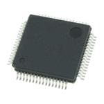
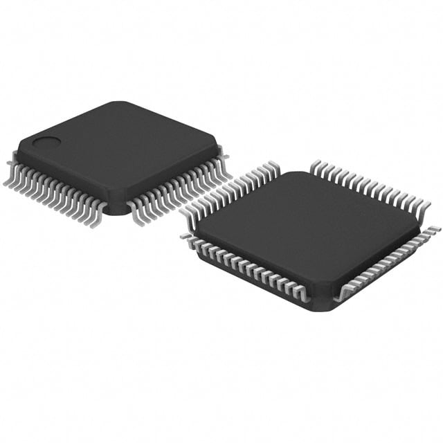
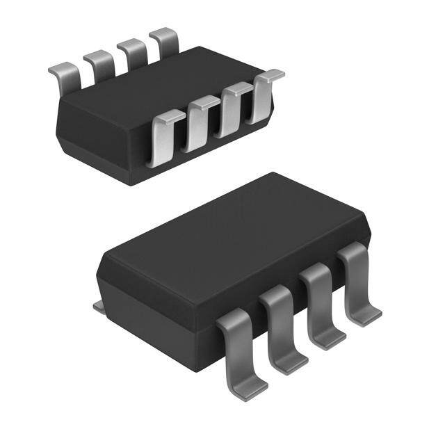
| 描述 | IC MCU ARM 256KB FLASH 64LQFP |
| EEPROM容量 | 4K x 8 |
| 产品分类 | |
| I/O数 | 44 |
| 品牌 | Freescale Semiconductor |
| 数据手册 | 点击此处下载产品Datasheet点击此处下载产品Datasheet点击此处下载产品Datasheet点击此处下载产品Datasheet点击此处下载产品Datasheethttp://cache.freescale.com/files/microcontrollers/doc/errata/KINETIS_1N89E.pdf?fpsp=1&WT_TYPE=Errata&WT_VENDOR=FREESCALE&WT_FILE_FORMAT=pdf&WT_ASSET=Documentation |
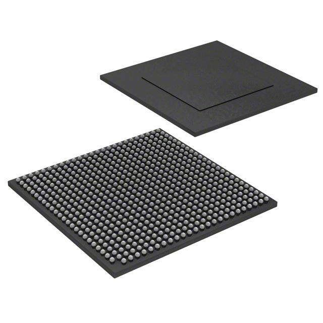
| 产品图片 |
|
| 产品型号 | MK12DX256VLH5 |
| PCN设计/规格 | http://cache.freescale.com/files/shared/doc/pcn/PCN15823.htmhttp://cache.freescale.com/files/shared/doc/pcn/PCN15928.htmhttp://cache.freescale.com/files/shared/doc/pcn/PCN16041.htm |
| RAM容量 | 32K x 8 |
| rohs | 无铅 / 符合限制有害物质指令(RoHS)规范要求 |
| 产品系列 | Kinetis K10 |
| 供应商器件封装 | 64-LQFP(10x10) |
| 包装 | 托盘 |
| 外设 | DMA, I²S, LVD, POR, PWM, WDT |
| 封装/外壳 | 64-LQFP |
| 工作温度 | -40°C ~ 105°C |
| 振荡器类型 | 内部 |
| 数据转换器 | A/D 22x16b,D/A 1x12b |
| 标准包装 | 160 |
| 核心处理器 | ARM® Cortex®-M4 |
| 核心尺寸 | 32-位 |
| 电压-电源(Vcc/Vdd) | 1.71 V ~ 3.6 V |
| 程序存储器类型 | 闪存 |
| 程序存储容量 | 256KB(256K x 8) |
| 连接性 | I²C, IrDA, SPI, UART/USART |
| 速度 | 50MHz |


- 商务部:美国ITC正式对集成电路等产品启动337调查
- 曝三星4nm工艺存在良率问题 高通将骁龙8 Gen1或转产台积电
- 太阳诱电将投资9.5亿元在常州建新厂生产MLCC 预计2023年完工
- 英特尔发布欧洲新工厂建设计划 深化IDM 2.0 战略
- 台积电先进制程称霸业界 有大客户加持明年业绩稳了
- 达到5530亿美元!SIA预计今年全球半导体销售额将创下新高
- 英特尔拟将自动驾驶子公司Mobileye上市 估值或超500亿美元
- 三星加码芯片和SET,合并消费电子和移动部门,撤换高东真等 CEO
- 三星电子宣布重大人事变动 还合并消费电子和移动部门
- 海关总署:前11个月进口集成电路产品价值2.52万亿元 增长14.8%


PDF Datasheet 数据手册内容提取
Freescale Semiconductor Document Number: K12P64M50SF4 Data Sheet: Technical Data Rev. 4, 08/2013 K12P64M50SF4 K12 Sub-Family Supports the following: MK12DX128VLH5, MK12DX256VLH5, MK12DN512VLH5 Features • Security and integrity modules • Operating Characteristics – Hardware CRC module to support fast cyclic – Voltage range: 1.71 to 3.6 V redundancy checks – Flash write voltage range: 1.71 to 3.6 V – 128-bit unique identification (ID) number per chip – Temperature range (ambient): -40 to 105°C • Human-machine interface • Performance – General-purpose input/output – Up to 50 MHz ARM Cortex-M4 core with DSP instructions delivering 1.25 Dhrystone MIPS per • Analog modules MHz – 16-bit SAR ADC – 12-bit DAC • Memories and memory interfaces – Two analog comparators (CMP) containing a 6-bit – Up to 512 KB of program flash for devices without DAC and programmable reference input FlexNVM. – Voltage reference – Up to 256 KB program flash for devices with FlexNVM. • Timers – 64 KB FlexNVM on FlexMemory devices – Programmable delay block – 4 KB FlexRAM on FlexMemory devices – Eight-channel motor control/general purpose/PWM – Up to 64 KB RAM timer – Serial programming interface (EzPort) – Two 2-channel general purpose timers, one with quadrature decoder functionality • Clocks – Periodic interrupt timers – 3 to 32 MHz crystal oscillator – 16-bit low-power timer – 32 kHz crystal oscillator – Carrier modulator transmitter – Multi-purpose clock generator – Real-time clock • System peripherals • Communication interfaces – Multiple low-power modes to provide power – USB Device Charger detect optimization based on application requirements – SPI module – 16-channel DMA controller, supporting up to 63 – Two I2C modules request sources – Four UART modules – External watchdog monitor – I2S module – Software watchdog – Low-leakage wakeup unit Freescale reserves the right to change the detail specifications as may be required to permit improvements in the design of its products. © 2012–2013 Freescale Semiconductor, Inc.
Table of Contents 1 Ordering parts...........................................................................3 5.4 Thermal specifications.......................................................20 1.1 Determining valid orderable parts......................................3 5.4.1 Thermal operating requirements...........................21 2 Part identification......................................................................3 5.4.2 Thermal attributes.................................................21 2.1 Description.........................................................................3 6 Peripheral operating requirements and behaviors....................22 2.2 Format...............................................................................3 6.1 Core modules....................................................................22 2.3 Fields.................................................................................3 6.1.1 JTAG electricals....................................................22 2.4 Example............................................................................4 6.2 System modules................................................................25 2.5 Small package marking.....................................................4 6.3 Clock modules...................................................................25 3 Terminology and guidelines......................................................5 6.3.1 MCG specifications...............................................25 3.1 Definition: Operating requirement......................................5 6.3.2 Oscillator electrical specifications.........................27 3.2 Definition: Operating behavior...........................................5 6.3.3 32 kHz oscillator electrical characteristics.............29 3.3 Definition: Attribute............................................................6 6.4 Memories and memory interfaces.....................................30 3.4 Definition: Rating...............................................................6 6.4.1 Flash electrical specifications................................30 3.5 Result of exceeding a rating..............................................7 6.4.2 EzPort switching specifications.............................33 3.6 Relationship between ratings and operating 6.5 Security and integrity modules..........................................34 requirements......................................................................7 6.6 Analog...............................................................................34 3.7 Guidelines for ratings and operating requirements............8 6.6.1 ADC electrical specifications.................................34 3.8 Definition: Typical value.....................................................8 6.6.2 CMP and 6-bit DAC electrical specifications.........38 3.9 Typical value conditions....................................................9 6.6.3 12-bit DAC electrical characteristics.....................41 4 Ratings......................................................................................9 6.6.4 Voltage reference electrical specifications............44 4.1 Thermal handling ratings...................................................9 6.7 Timers................................................................................45 4.2 Moisture handling ratings..................................................10 6.8 Communication interfaces.................................................45 4.3 ESD handling ratings.........................................................10 6.8.1 DSPI switching specifications (limited voltage 4.4 Voltage and current operating ratings...............................10 range)....................................................................45 5 General.....................................................................................10 6.8.2 DSPI switching specifications (full voltage range).47 5.1 AC electrical characteristics..............................................11 6.8.3 I2C switching specifications..................................49 5.2 Nonswitching electrical specifications...............................11 6.8.4 UART switching specifications..............................49 5.2.1 Voltage and current operating requirements.........11 6.8.5 Normal Run, Wait and Stop mode performance 5.2.2 LVD and POR operating requirements.................12 over the full operating voltage range.....................49 5.2.3 Voltage and current operating behaviors..............13 6.8.6 VLPR, VLPW, and VLPS mode performance 5.2.4 Power mode transition operating behaviors..........13 over the full operating voltage range.....................51 5.2.5 Power consumption operating behaviors..............14 7 Dimensions...............................................................................53 5.2.6 EMC radiated emissions operating behaviors.......18 7.1 Obtaining package dimensions.........................................53 5.2.7 Designing with radiated emissions in mind...........19 8 Pinout........................................................................................53 5.2.8 Capacitance attributes..........................................19 8.1 K12 Signal Multiplexing and Pin Assignments..................53 5.3 Switching specifications.....................................................19 8.2 K12 Pinouts.......................................................................56 5.3.1 Device clock specifications...................................19 9 Revision History........................................................................57 5.3.2 General switching specifications...........................20 K12 Sub-Family Data Sheet, Rev. 4, 08/2013. 2 Freescale Semiconductor, Inc.
Ordering parts 1 Ordering parts 1.1 Determining valid orderable parts Valid orderable part numbers are provided on the web. To determine the orderable part numbers for this device, go to freescale.com and perform a part number search for the following device numbers: PK12 and MK12 . 2 Part identification 2.1 Description Part numbers for the chip have fields that identify the specific part. You can use the values of these fields to determine the specific part you have received. 2.2 Format Part numbers for this device have the following format: Q K## A M FFF R T PP CC N 2.3 Fields This table lists the possible values for each field in the part number (not all combinations are valid): Field Description Values Q Qualification status • M = Fully qualified, general market flow • P = Prequalification K## Kinetis family • K12 A Key attribute • D = Cortex-M4 w/ DSP • F = Cortex-M4 w/ DSP and FPU M Flash memory type • N = Program flash only • X = Program flash and FlexMemory Table continues on the next page... K12 Sub-Family Data Sheet, Rev. 4, 08/2013. Freescale Semiconductor, Inc. 3
Part identification Field Description Values FFF Program flash memory size • 32 = 32 KB • 64 = 64 KB • 128 = 128 KB • 256 = 256 KB • 512 = 512 KB • 1M0 = 1 MB • 2M0 = 2 MB R Silicon revision • Z = Initial • (Blank) = Main • A = Revision after main T Temperature range (°C) • V = –40 to 105 • C = –40 to 85 PP Package identifier • FM = 32 QFN (5 mm x 5 mm) • FT = 48 QFN (7 mm x 7 mm) • LF = 48 LQFP (7 mm x 7 mm) • LH = 64 LQFP (10 mm x 10 mm) • MP = 64 MAPBGA (5 mm x 5 mm) • LK = 80 LQFP (12 mm x 12 mm) • LL = 100 LQFP (14 mm x 14 mm) • MC = 121 MAPBGA (8 mm x 8 mm) • LQ = 144 LQFP (20 mm x 20 mm) • MD = 144 MAPBGA (13 mm x 13 mm) CC Maximum CPU frequency (MHz) • 5 = 50 MHz • 7 = 72 MHz • 10 = 100 MHz • 12 = 120 MHz • 15 = 150 MHz • 18 = 180 MHz N Packaging type • R = Tape and reel • (Blank) = Trays 2.4 Example This is an example part number: MK12DN512VLH5 2.5 Small package marking In an effort to save space, small package devices use special marking on the chip. These markings have the following format: Q ## C F T PP This table lists the possible values for each field in the part number for small packages (not all combinations are valid): K12 Sub-Family Data Sheet, Rev. 4, 08/2013. 4 Freescale Semiconductor, Inc.
Terminology and guidelines Field Description Values Q Qualification status • M = Fully qualified, general market flow • P = Prequalification C Speed • G = 50 MHz F Flash memory configuration • G = 128 KB + Flex • H = 256 KB + Flex • 9 = 512 KB T Temperature range (°C) • V = –40 to 105 PP Package identifier • MC = 121 MAPBGA This tables lists some examples of small package marking along with the original part numbers: Original part number Alternate part number MK12DX256VLF5 M12GHVLF MK12DN512VLH5 M12G9VLH 3 Terminology and guidelines 3.1 Definition: Operating requirement An operating requirement is a specified value or range of values for a technical characteristic that you must guarantee during operation to avoid incorrect operation and possibly decreasing the useful life of the chip. 3.1.1 Example This is an example of an operating requirement: Symbol Description Min. Max. Unit V 1.0 V core supply 0.9 1.1 V DD voltage K12 Sub-Family Data Sheet, Rev. 4, 08/2013. Freescale Semiconductor, Inc. 5
Terminology and guidelines 3.2 Definition: Operating behavior An operating behavior is a specified value or range of values for a technical characteristic that are guaranteed during operation if you meet the operating requirements and any other specified conditions. 3.2.1 Example This is an example of an operating behavior: Symbol Description Min. Max. Unit I Digital I/O weak pullup/ 10 130 µA WP pulldown current 3.3 Definition: Attribute An attribute is a specified value or range of values for a technical characteristic that are guaranteed, regardless of whether you meet the operating requirements. 3.3.1 Example This is an example of an attribute: Symbol Description Min. Max. Unit CIN_D Input capacitance: — 7 pF digital pins 3.4 Definition: Rating A rating is a minimum or maximum value of a technical characteristic that, if exceeded, may cause permanent chip failure: • Operating ratings apply during operation of the chip. • Handling ratings apply when the chip is not powered. K12 Sub-Family Data Sheet, Rev. 4, 08/2013. 6 Freescale Semiconductor, Inc.
Terminology and guidelines 3.4.1 Example This is an example of an operating rating: Symbol Description Min. Max. Unit V 1.0 V core supply –0.3 1.2 V DD voltage 3.5 Result of exceeding a rating 40 m) 30 p p e ( s in tim 20 Tsohoen l ikaesl iah ocohda roafc pteerrimstiacn beengt icnhsi pto f aeixlucreee idn corneea soef sit sra oppidelrya atins g ratings. e ur Fail 10 0 Operating rating Measured characteristic 3.6 Relationship between ratings and operating requirements O perating rating (min.) O perating require m ent (min.) O perating require m ent (m ax.) O perating rating (m ax.) Fatal range Degraded operating range Normal operating range Degraded operating range Fatal range Expected permanent failure - No permanent failure - No permanent failure - No permanent failure Expected permanent failure - Possible decreased life - Correct operation - Possible decreased life - Possible incorrect operation - Possible incorrect operation –∞ ∞ Operating (power on) H andling rating (min.) H andling rating (m ax.) Fatal range Handling range Fatal range Expected permanent failure No permanent failure Expected permanent failure –∞ ∞ Handling (power off) K12 Sub-Family Data Sheet, Rev. 4, 08/2013. Freescale Semiconductor, Inc. 7
Terminology and guidelines 3.7 Guidelines for ratings and operating requirements Follow these guidelines for ratings and operating requirements: • Never exceed any of the chip’s ratings. • During normal operation, don’t exceed any of the chip’s operating requirements. • If you must exceed an operating requirement at times other than during normal operation (for example, during power sequencing), limit the duration as much as possible. 3.8 Definition: Typical value A typical value is a specified value for a technical characteristic that: • Lies within the range of values specified by the operating behavior • Given the typical manufacturing process, is representative of that characteristic during operation when you meet the typical-value conditions or other specified conditions Typical values are provided as design guidelines and are neither tested nor guaranteed. 3.8.1 Example 1 This is an example of an operating behavior that includes a typical value: Symbol Description Min. Typ. Max. Unit I Digital I/O weak 10 70 130 µA WP pullup/pulldown current 3.8.2 Example 2 This is an example of a chart that shows typical values for various voltage and temperature conditions: K12 Sub-Family Data Sheet, Rev. 4, 08/2013. 8 Freescale Semiconductor, Inc.
Ratings 5000 4500 4000 T 3500 J 150 °C A) 3000 μ ( 105 °C P O 2500 T S 25 °C _ D ID 2000 –40 °C 1500 1000 500 0 0.90 0.95 1.00 1.05 1.10 V (V) DD 3.9 Typical value conditions Typical values assume you meet the following conditions (or other conditions as specified): Symbol Description Value Unit T Ambient temperature 25 °C A V 3.3 V supply voltage 3.3 V DD 4 Ratings 4.1 Thermal handling ratings Symbol Description Min. Max. Unit Notes T Storage temperature –55 150 °C 1 STG T Solder temperature, lead-free — 260 °C 2 SDR 1. Determined according to JEDEC Standard JESD22-A103, High Temperature Storage Life. 2. Determined according to IPC/JEDEC Standard J-STD-020, Moisture/Reflow Sensitivity Classification for Nonhermetic Solid State Surface Mount Devices. K12 Sub-Family Data Sheet, Rev. 4, 08/2013. Freescale Semiconductor, Inc. 9
General 4.2 Moisture handling ratings Symbol Description Min. Max. Unit Notes MSL Moisture sensitivity level — 3 — 1 1. Determined according to IPC/JEDEC Standard J-STD-020, Moisture/Reflow Sensitivity Classification for Nonhermetic Solid State Surface Mount Devices. 4.3 ESD handling ratings Symbol Description Min. Max. Unit Notes V Electrostatic discharge voltage, human body model -2000 +2000 V 1 HBM V Electrostatic discharge voltage, charged-device model -500 +500 V 2 CDM I Latch-up current at ambient temperature of 105°C -100 +100 mA 3 LAT 1. Determined according to JEDEC Standard JESD22-A114, Electrostatic Discharge (ESD) Sensitivity Testing Human Body Model (HBM). 2. Determined according to JEDEC Standard JESD22-C101, Field-Induced Charged-Device Model Test Method for Electrostatic-Discharge-Withstand Thresholds of Microelectronic Components. 3. Determined according to JEDEC Standard JESD78, IC Latch-Up Test. 4.4 Voltage and current operating ratings Symbol Description Min. Max. Unit V Digital supply voltage –0.3 3.8 V DD I Digital supply current — 155 mA DD V Digital input voltage (except RESET, EXTAL, and XTAL) –0.3 V DIO V Analog1, RESET, EXTAL, and XTAL input voltage –0.3 V + 0.3 V AIO DD I Maximum current single pin limit (applies to all digital pins) –25 25 mA D V Analog supply voltage V – 0.3 V + 0.3 V DDA DD DD VREGIN USB regulator input –0.3 6.0 V V RTC battery supply voltage –0.3 3.8 V BAT 1. Analog pins are defined as pins that do not have an associated general purpose I/O port function. 5 General K12 Sub-Family Data Sheet, Rev. 4, 08/2013. 10 Freescale Semiconductor, Inc.
General 5.1 AC electrical characteristics Unless otherwise specified, propagation delays are measured from the 50% to the 50% point, and rise and fall times are measured at the 20% and 80% points, as shown in the following figure. Figure 1. Input signal measurement reference 5.2 Nonswitching electrical specifications 5.2.1 Voltage and current operating requirements Table 1. Voltage and current operating requirements Symbol Description Min. Max. Unit Notes V Supply voltage 1.71 3.6 V DD V Analog supply voltage 1.71 3.6 V DDA V – V V -to-V differential voltage –0.1 0.1 V DD DDA DD DDA V – V V -to-V differential voltage –0.1 0.1 V SS SSA SS SSA V RTC battery supply voltage 1.71 3.6 V BAT V Input high voltage IH • 2.7 V ≤ V ≤ 3.6 V 0.7 × V — V DD DD • 1.7 V ≤ V ≤ 2.7 V 0.75 × V — V DD DD V Input low voltage IL • 2.7 V ≤ V ≤ 3.6 V — 0.35 × V V DD DD • 1.7 V ≤ V ≤ 2.7 V — 0.3 × V V DD DD V Input hysteresis 0.06 × V — V HYS DD I I/O pin DC injection current — single pin 1 ICIO • V < V -0.3V (Negative current injection) mA IN SS -3 — • V > V +0.3V (Positive current injection) IN DD — +3 Table continues on the next page... K12 Sub-Family Data Sheet, Rev. 4, 08/2013. Freescale Semiconductor, Inc. 11
General Table 1. Voltage and current operating requirements (continued) Symbol Description Min. Max. Unit Notes I Contiguous pin DC injection current —regional limit, ICcont includes sum of negative injection currents or sum of positive injection currents of 16 contiguous pins -25 — mA • Negative current injection — +25 • Positive current injection V V voltage required to retain RAM 1.2 — V RAM DD V V voltage required to retain the VBAT register file V — V RFVBAT BAT POR_VBAT 1. All analog pins are internally clamped to V and V through ESD protection diodes. If V is less than V or greater SS DD IN AIO_MIN than V , a current limiting resistor is required. The negative DC injection current limiting resistor is calculated as AIO_MAX R=(V -V )/|I |. The positive injection current limiting resistor is calculated as R=(V -V )/|I |. Select the AIO_MIN IN ICAIO IN AIO_MAX ICAIO larger of these two calculated resistances if the pin is exposed to positive and negative injection currents. 5.2.2 LVD and POR operating requirements Table 2. V supply LVD and POR operating requirements DD Symbol Description Min. Typ. Max. Unit Notes V Falling VDD POR detect voltage 0.8 1.1 1.5 V POR V Falling low-voltage detect threshold — high 2.48 2.56 2.64 V LVDH range (LVDV=01) Low-voltage warning thresholds — high range 1 V • Level 1 falling (LVWV=00) 2.62 2.70 2.78 V LVW1H V • Level 2 falling (LVWV=01) 2.72 2.80 2.88 V LVW2H V • Level 3 falling (LVWV=10) 2.82 2.90 2.98 V LVW3H V • Level 4 falling (LVWV=11) 2.92 3.00 3.08 V LVW4H V Low-voltage inhibit reset/recover hysteresis — — 80 — mV HYSH high range V Falling low-voltage detect threshold — low range 1.54 1.60 1.66 V LVDL (LVDV=00) Low-voltage warning thresholds — low range 1 V • Level 1 falling (LVWV=00) 1.74 1.80 1.86 V LVW1L V • Level 2 falling (LVWV=01) 1.84 1.90 1.96 V LVW2L V • Level 3 falling (LVWV=10) 1.94 2.00 2.06 V LVW3L V • Level 4 falling (LVWV=11) 2.04 2.10 2.16 V LVW4L V Low-voltage inhibit reset/recover hysteresis — — 60 — mV HYSL low range V Bandgap voltage reference 0.97 1.00 1.03 V BG t Internal low power oscillator period — factory 900 1000 1100 μs LPO trimmed K12 Sub-Family Data Sheet, Rev. 4, 08/2013. 12 Freescale Semiconductor, Inc.
General 1. Rising threshold is the sum of falling threshold and hysteresis voltage Table 3. VBAT power operating requirements Symbol Description Min. Typ. Max. Unit Notes V Falling VBAT supply POR detect voltage 0.8 1.1 1.5 V POR_VBAT 5.2.3 Voltage and current operating behaviors Table 4. Voltage and current operating behaviors Symbol Description Min. Max. Unit Notes V Output high voltage — high drive strength OH • 2.7 V ≤ V ≤ 3.6 V, I = - 9 mA V – 0.5 — V DD OH DD • 1.71 V ≤ V ≤ 2.7 V, I = -3 mA V – 0.5 — V DD OH DD Output high voltage — low drive strength • 2.7 V ≤ V ≤ 3.6 V, I = -2 mA V – 0.5 — V DD OH DD • 1.71 V ≤ V ≤ 2.7 V, I = -0.6 mA V – 0.5 — V DD OH DD I Output high current total for all ports — 100 mA OHT V Output low voltage — high drive strength OL • 2.7 V ≤ V ≤ 3.6 V, I = 9 mA — 0.5 V DD OL • 1.71 V ≤ V ≤ 2.7 V, I = 3 mA — 0.5 V DD OL Output low voltage — low drive strength • 2.7 V ≤ V ≤ 3.6 V, I = 2 mA — 0.5 V DD OL • 1.71 V ≤ V ≤ 2.7 V, I = 0.6 mA — 0.5 V DD OL I Output low current total for all ports — 100 mA OLT I Input leakage current (per pin) IN • @ full temperature range — 1.0 μA 1 • @ 25 °C — 0.1 μA I Hi-Z (off-state) leakage current (per pin) — 1 μA OZ I Total Hi-Z (off-state) leakage current (all input pins) — 4 μA OZ R Internal pullup resistors 22 50 kΩ 2 PU R Internal pulldown resistors 22 50 kΩ 3 PD 1. Tested by ganged leakage method 2. Measured at Vinput = V SS 3. Measured at Vinput = V DD K12 Sub-Family Data Sheet, Rev. 4, 08/2013. Freescale Semiconductor, Inc. 13
General 5.2.4 Power mode transition operating behaviors All specifications except t , and VLLSx→RUN recovery times in the following table POR assume this clock configuration: • CPU and system clocks = 50 MHz • Bus clock = 50 MHz • Flash clock = 25 MHz • MCG mode: FEI Table 5. Power mode transition operating behaviors Symbol Description Min. Max. Unit Notes t After a POR event, amount of time from the point V μs 1 POR DD reaches 1.71 V to execution of the first instruction across the operating temperature range of the chip. — 300 • 1.71 V/(VDD slew rate) ≤ 300 μs — 1.7 V / (V • 1.71 V/(V slew rate) > 300 μs DD DD slew rate) — 135 μs • VLLS0 → RUN — 135 μs • VLLS1 → RUN — 85 μs • VLLS2 → RUN — 85 μs • VLLS3 → RUN — 6 μs • LLS → RUN — 5.2 μs • VLPS → RUN — 5.2 μs • STOP → RUN 1. Normal boot (FTFL_OPT[LPBOOT]=1) 5.2.5 Power consumption operating behaviors Table 6. Power consumption operating behaviors Symbol Description Min. Typ. Max. Unit Notes I Analog supply current — — See note mA 1 DDA I Run mode current — all peripheral clocks 2 DD_RUN disabled, code executing from flash • @ 1.8 V — 12.98 14 mA • @ 3.0 V — 12.93 13.8 mA Table continues on the next page... K12 Sub-Family Data Sheet, Rev. 4, 08/2013. 14 Freescale Semiconductor, Inc.
General Table 6. Power consumption operating behaviors (continued) Symbol Description Min. Typ. Max. Unit Notes I Run mode current — all peripheral clocks 3, 4 DD_RUN enabled, code executing from flash • @ 1.8 V — 17.04 19.3 mA • @ 3.0 V • @ 25°C — 17.01 18.9 mA • @ 125°C — 19.8 21.3 mA I Wait mode high frequency current at 3.0 V — all — 7.95 9.5 mA 2 DD_WAIT peripheral clocks disabled I Wait mode reduced frequency current at 3.0 V — — 5.88 7.4 mA 5 DD_WAIT all peripheral clocks disabled I Stop mode current at 3.0 V — μA DD_STOP 320 436 • @ –40 to 25°C • @ 50°C 360 489 • @ 70°C 410 620 • @ 105°C 610 1100 I Very-low-power run mode current at 3.0 V — all — 754 — μA 6 DD_VLPR peripheral clocks disabled I Very-low-power run mode current at 3.0 V — all — 1.1 — mA 7 DD_VLPR peripheral clocks enabled I Very-low-power wait mode current at 3.0 V — 437 — μA 8 DD_VLPW I Very-low-power stop mode current at 3.0 V — μA DD_VLPS 7.33 24.2 • @ –40 to 25°C • @ 50°C 14 32 • @ 70°C 28 48 • @ 105°C 110 280 I Low leakage stop mode current at 3.0 V — μA DD_LLS 3.14 4.8 • @ –40 to 25°C • @ 50°C 6.48 28.3 • @ 70°C 13.85 44.6 • @ 105°C 55.53 71.3 I Very low-leakage stop mode 3 current at 3.0 V μA DD_VLLS3 — 2.19 3.4 • @ –40 to 25°C 4.35 4.35 • @ 50°C • @ 70°C 8.92 24.6 • @ 105°C 35.33 45.3 I Very low-leakage stop mode 2 current at 3.0 V — μA DD_VLLS2 1.77 3.1 • @ –40 to 25°C • @ 50°C 2.81 13.8 • @ 70°C 5.20 22.3 • @ 105°C 19.88 34.2 Table continues on the next page... K12 Sub-Family Data Sheet, Rev. 4, 08/2013. Freescale Semiconductor, Inc. 15
General Table 6. Power consumption operating behaviors (continued) Symbol Description Min. Typ. Max. Unit Notes I Very low-leakage stop mode 1 current at 3.0 V — μA DD_VLLS1 1.03 1.8 • @ –40 to 25°C • @ 50°C 1.92 7.5 • @ 70°C 4.03 15.9 • @ 105°C 17.43 28.7 I Very low-leakage stop mode 0 current at 3.0 V — μA DD_VLLS0 0.543 1.1 with POR detect circuit enabled • @ –40 to 25°C 1.36 7.58 • @ 50°C 3.39 14.3 • @ 70°C • @ 105°C 16.52 24.1 I Very low-leakage stop mode 0 current at 3.0 V — μA DD_VLLS0 0.359 0.95 with POR detect circuit disabled • @ –40 to 25°C 1.03 6.8 • @ 50°C 2.87 15.4 • @ 70°C • @ 105°C 15.20 25.3 I Average current when CPU is not accessing RTC — μA 9 DD_VBAT 0.91 1.1 registers at 3.0 V • @ –40 to 25°C 1.1 1.35 • @ 50°C 1.5 1.85 • @ 70°C • @ 105°C 4.3 5.7 1. The analog supply current is the sum of the active or disabled current for each of the analog modules on the device. See each module's specification for its supply current. 2. 50 MHz core and system clock, 25 MHz bus clock, and 25 MHz flash clock. MCG configured for FEI mode. All peripheral clocks disabled. 3. 50 MHz core and system clock, 25 MHz bus clock, and 25 MHz flash clock. MCG configured for FEI mode. All peripheral clocks enabled, and peripherals are in active operation. 4. Max values are measured with CPU executing DSP instructions 5. 25 MHz core and system clock, 25 MHz bus clock, and 12.5 MHz flash clock. MCG configured for FEI mode. 6. 4 MHz core, system, and bus clock and 1 MHz flash clock. MCG configured for BLPE mode. All peripheral clocks disabled. Code executing from flash. 7. 4 MHz core, system, and bus clock and 1 MHz flash clock. MCG configured for BLPE mode. All peripheral clocks enabled but peripherals are not in active operation. Code executing from flash. 8. 4 MHz core, system, and bus clock and 1 MHz flash clock. MCG configured for BLPE mode. All peripheral clocks disabled. 9. Includes 32 kHz oscillator current and RTC operation. 5.2.5.1 Diagram: Typical IDD_RUN operating behavior The following data was measured under these conditions: • MCG in FBE mode • USB regulator disabled • No GPIOs toggled • Code execution from flash with cache enabled • For the ALLOFF curve, all peripheral clocks are disabled except FTFL K12 Sub-Family Data Sheet, Rev. 4, 08/2013. 16 Freescale Semiconductor, Inc.
General Figure 2. Run mode supply current vs. core frequency K12 Sub-Family Data Sheet, Rev. 4, 08/2013. Freescale Semiconductor, Inc. 17
General Figure 3. VLPR mode supply current vs. core frequency 5.2.6 EMC radiated emissions operating behaviors Table 7. EMC radiated emissions operating behaviors 1 Symbol Description Frequency Typ. Unit Notes band (MHz) V Radiated emissions voltage, band 1 0.15–50 19 dBμV 2, 3 RE1 V Radiated emissions voltage, band 2 50–150 21 dBμV RE2 V Radiated emissions voltage, band 3 150–500 19 dBμV RE3 V Radiated emissions voltage, band 4 500–1000 11 dBμV RE4 V IEC level 0.15–1000 L — 3, 4 RE_IEC 1. This data was collected on a MK20DN128VLH5 64pin LQFP device. 2. Determined according to IEC Standard 61967-1, Integrated Circuits - Measurement of Electromagnetic Emissions, 150 kHz to 1 GHz Part 1: General Conditions and Definitions and IEC Standard 61967-2, Integrated Circuits - Measurement of Electromagnetic Emissions, 150 kHz to 1 GHz Part 2: Measurement of Radiated Emissions—TEM Cell and Wideband TEM Cell Method. Measurements were made while the microcontroller was running basic application code. The reported emission level is the value of the maximum measured emission, rounded up to the next whole number, from among the measured orientations in each frequency range. K12 Sub-Family Data Sheet, Rev. 4, 08/2013. 18 Freescale Semiconductor, Inc.
General 3. V = 3.3 V, T = 25 °C, f = 12 MHz (crystal), f = 48 MHz, f = 48MHz DD A OSC SYS BUS 4. Specified according to Annex D of IEC Standard 61967-2, Measurement of Radiated Emissions—TEM Cell and Wideband TEM Cell Method 5.2.7 Designing with radiated emissions in mind To find application notes that provide guidance on designing your system to minimize interference from radiated emissions: 1. Go to www.freescale.com. 2. Perform a keyword search for “EMC design.” 5.2.8 Capacitance attributes Table 8. Capacitance attributes Symbol Description Min. Max. Unit C Input capacitance: analog pins — 7 pF IN_A C Input capacitance: digital pins — 7 pF IN_D 5.3 Switching specifications 5.3.1 Device clock specifications Table 9. Device clock specifications Symbol Description Min. Max. Unit Notes Normal run mode f System and core clock — 50 MHz SYS f Bus clock — 50 MHz BUS f Flash clock — 25 MHz FLASH f LPTMR clock — 25 MHz LPTMR VLPR mode1 f System and core clock — 4 MHz SYS f Bus clock — 4 MHz BUS f Flash clock — 1 MHz FLASH f External reference clock — 16 MHz ERCLK f LPTMR clock — 25 MHz LPTMR_pin f LPTMR external reference clock — 16 MHz LPTMR_ERCLK f I2S master clock — 12.5 MHz I2S_MCLK f I2S bit clock — 4 MHz I2S_BCLK K12 Sub-Family Data Sheet, Rev. 4, 08/2013. Freescale Semiconductor, Inc. 19
General 1. The frequency limitations in VLPR mode here override any frequency specification listed in the timing specification for any other module. 5.3.2 General switching specifications These general purpose specifications apply to all pins configured for: • GPIO signaling • Other peripheral module signaling not explicitly stated elsewhere Table 10. General switching specifications Symbol Description Min. Max. Unit Notes GPIO pin interrupt pulse width (digital glitch filter 1.5 — Bus clock 1, 2 disabled) — Synchronous path cycles GPIO pin interrupt pulse width (digital glitch filter 100 — ns 3 disabled, analog filter enabled) — Asynchronous path GPIO pin interrupt pulse width (digital glitch filter 50 — ns 3 disabled, analog filter disabled) — Asynchronous path External reset pulse width (digital glitch filter disabled) 100 — ns 3 Port rise and fall time (high drive strength) 4 • Slew disabled • 1.71 ≤ V ≤ 2.7V — 13 ns DD • 2.7 ≤ V ≤ 3.6V — 7 ns DD • Slew enabled • 1.71 ≤ V ≤ 2.7V — 36 ns DD • 2.7 ≤ V ≤ 3.6V — 24 ns DD Port rise and fall time (low drive strength) 5 • Slew disabled • 1.71 ≤ V ≤ 2.7V — 12 ns DD • 2.7 ≤ V ≤ 3.6V — 6 ns DD • Slew enabled • 1.71 ≤ V ≤ 2.7V — 36 ns DD • 2.7 ≤ V ≤ 3.6V — 24 ns DD 1. This is the minimum pulse width that is guaranteed to pass through the pin synchronization circuitry. Shorter pulses may or may not be recognized. In Stop, VLPS, LLS, and VLLSx modes, the synchronizer is bypassed so shorter pulses can be recognized in that case. 2. The greater synchronous and asynchronous timing must be met. 3. This is the minimum pulse width that is guaranteed to be recognized as a pin interrupt request in Stop, VLPS, LLS, and VLLSx modes. 4. 75 pF load 5. 15 pF load K12 Sub-Family Data Sheet, Rev. 4, 08/2013. 20 Freescale Semiconductor, Inc.
General 5.4 Thermal specifications 5.4.1 Thermal operating requirements Table 11. Thermal operating requirements Symbol Description Min. Max. Unit T Die junction temperature –40 125 °C J T Ambient temperature –40 105 °C A 5.4.2 Thermal attributes Board type Symbol Description 64 LQFP Unit Notes Single-layer (1s) R Thermal 65 °C/W 1, 2 θJA resistance, junction to ambient (natural convection) Four-layer (2s2p) R Thermal 46 °C/W 1, 3 θJA resistance, junction to ambient (natural convection) Single-layer (1s) R Thermal 53 °C/W 1,3 θJMA resistance, junction to ambient (200 ft./ min. air speed) Four-layer (2s2p) R Thermal 40 °C/W 1,3 θJMA resistance, junction to ambient (200 ft./ min. air speed) — R Thermal 28 °C/W 4 θJB resistance, junction to board — R Thermal 15 °C/W 5 θJC resistance, junction to case — Ψ Thermal 3 °C/W 6 JT characterization parameter, junction to package top outside center (natural convection) 1. Junction temperature is a function of die size, on-chip power dissipation, package thermal resistance, mounting site (board) temperature, ambient temperature, air flow, power dissipation of other components on the board, and board thermal resistance. 2. Determined according to JEDEC Standard JESD51-2, Integrated Circuits Thermal Test Method Environmental Conditions—Natural Convection (Still Air) with the single layer board horizontal. For the LQFP, the board meets the JESD51-3 specification. For the MAPBGA, the board meets the JESD51-9 specification. K12 Sub-Family Data Sheet, Rev. 4, 08/2013. Freescale Semiconductor, Inc. 21
Peripheral operating requirements and behaviors 3. Determined according to JEDEC Standard JESD51-6, Integrated Circuits Thermal Test Method Environmental Conditions—Forced Convection (Moving Air) with the board horizontal. 4. Determined according to JEDEC Standard JESD51-8, Integrated Circuit Thermal Test Method Environmental Conditions—Junction-to-Board. Board temperature is measured on the top surface of the board near the package. 5. Determined according to Method 1012.1 of MIL-STD 883, Test Method Standard, Microcircuits, with the cold plate temperature used for the case temperature. The value includes the thermal resistance of the interface material between the top of the package and the cold plate. 6. Determined according to JEDEC Standard JESD51-2, Integrated Circuits Thermal Test Method Environmental Conditions—Natural Convection (Still Air). 6 Peripheral operating requirements and behaviors 6.1 Core modules 6.1.1 JTAG electricals Table 12. JTAG limited voltage range electricals Symbol Description Min. Max. Unit Operating voltage 2.7 3.6 V J1 TCLK frequency of operation MHz • Boundary Scan 0 10 • JTAG and CJTAG 0 25 • Serial Wire Debug 0 50 J2 TCLK cycle period 1/J1 — ns J3 TCLK clock pulse width • Boundary Scan 50 — ns • JTAG and CJTAG 20 — ns • Serial Wire Debug 10 — ns J4 TCLK rise and fall times — 3 ns J5 Boundary scan input data setup time to TCLK rise 20 — ns J6 Boundary scan input data hold time after TCLK rise 0 — ns J7 TCLK low to boundary scan output data valid — 25 ns J8 TCLK low to boundary scan output high-Z — 25 ns J9 TMS, TDI input data setup time to TCLK rise 8 — ns J10 TMS, TDI input data hold time after TCLK rise 1 — ns J11 TCLK low to TDO data valid — 17 ns J12 TCLK low to TDO high-Z — 17 ns J13 TRST assert time 100 — ns J14 TRST setup time (negation) to TCLK high 8 — ns K12 Sub-Family Data Sheet, Rev. 4, 08/2013. 22 Freescale Semiconductor, Inc.
Peripheral operating requirements and behaviors Table 13. JTAG full voltage range electricals Symbol Description Min. Max. Unit Operating voltage 1.71 3.6 V J1 TCLK frequency of operation MHz • Boundary Scan 0 10 • JTAG and CJTAG 0 20 • Serial Wire Debug 0 40 J2 TCLK cycle period 1/J1 — ns J3 TCLK clock pulse width • Boundary Scan 50 — ns • JTAG and CJTAG 25 — ns • Serial Wire Debug 12.5 — ns J4 TCLK rise and fall times — 3 ns J5 Boundary scan input data setup time to TCLK rise 20 — ns J6 Boundary scan input data hold time after TCLK rise 0 — ns J7 TCLK low to boundary scan output data valid — 25 ns J8 TCLK low to boundary scan output high-Z — 25 ns J9 TMS, TDI input data setup time to TCLK rise 8 — ns J10 TMS, TDI input data hold time after TCLK rise 1.4 — ns J11 TCLK low to TDO data valid — 22.1 ns J12 TCLK low to TDO high-Z — 22.1 ns J13 TRST assert time 100 — ns J14 TRST setup time (negation) to TCLK high 8 — ns J2 J3 J3 TCLK (input) J4 J4 Figure 4. Test clock input timing K12 Sub-Family Data Sheet, Rev. 4, 08/2013. Freescale Semiconductor, Inc. 23
Peripheral operating requirements and behaviors TCLK J5 J6 Data inputs Input data valid J7 Data outputs Output data valid J8 Data outputs J7 Data outputs Output data valid Figure 5. Boundary scan (JTAG) timing TCLK J9 J10 TDI/TMS Input data valid J11 TDO Output data valid J12 TDO J11 TDO Output data valid Figure 6. Test Access Port timing K12 Sub-Family Data Sheet, Rev. 4, 08/2013. 24 Freescale Semiconductor, Inc.
Peripheral operating requirements and behaviors TCLK J14 J13 TRST Figure 7. TRST timing 6.2 System modules There are no specifications necessary for the device's system modules. 6.3 Clock modules 6.3.1 MCG specifications Table 14. MCG specifications Symbol Description Min. Typ. Max. Unit Notes f Internal reference frequency (slow clock) — — 32.768 — kHz ints_ft factory trimmed at nominal VDD and 25 °C f Internal reference frequency (slow clock) — user 31.25 — 39.0625 kHz ints_t trimmed Δ Resolution of trimmed average DCO output — ± 0.3 ± 0.6 %f 1 fdco_res_t dco frequency at fixed voltage and temperature — using SCTRIM and SCFTRIM Δf Resolution of trimmed average DCO output — ± 0.2 ± 0.5 %f 1 dco_res_t dco frequency at fixed voltage and temperature — using SCTRIM only Δf Total deviation of trimmed average DCO output — +0.5/-0.7 ± 2 %f 1, 2 dco_t dco frequency over voltage and temperature Δf Total deviation of trimmed average DCO output — ± 0.3 ±1 %f 1, 2 dco_t dco frequency over fixed voltage and temperature range of 0–70°C f Internal reference frequency (fast clock) — — 4 — MHz intf_ft factory trimmed at nominal VDD and 25°C f Internal reference frequency (fast clock) — user 3 — 5 MHz intf_t trimmed at nominal VDD and 25 °C f Loss of external clock minimum frequency — (3/5) x — — kHz loc_low RANGE = 00 f ints_t f Loss of external clock minimum frequency — (16/5) x — — kHz loc_high RANGE = 01, 10, or 11 f ints_t Table continues on the next page... K12 Sub-Family Data Sheet, Rev. 4, 08/2013. Freescale Semiconductor, Inc. 25
Peripheral operating requirements and behaviors Table 14. MCG specifications (continued) Symbol Description Min. Typ. Max. Unit Notes FLL f FLL reference frequency range 31.25 — 39.0625 kHz fll_ref f DCO output Low range (DRS=00) 20 20.97 25 MHz 3, 4 dco frequency range 640 × f fll_ref Mid range (DRS=01) 40 41.94 50 MHz 1280 × f fll_ref Mid-high range (DRS=10) 60 62.91 75 MHz 1920 × f fll_ref High range (DRS=11) 80 83.89 100 MHz 2560 × f fll_ref f DCO output Low range (DRS=00) — 23.99 — MHz 5, 6 dco_t_DMX32 frequency 732 × f fll_ref Mid range (DRS=01) — 47.97 — MHz 1464 × f fll_ref Mid-high range (DRS=10) — 71.99 — MHz 2197 × f fll_ref High range (DRS=11) — 95.98 — MHz 2929 × f fll_ref J FLL period jitter ps cyc_fll — 180 — • f = 48 MHz DCO — 150 — • f = 98 MHz DCO t FLL target frequency acquisition time — — 1 ms 7 fll_acquire PLL f VCO operating frequency 48.0 — 100 MHz vco I PLL operating current 8 pll — 1060 — µA • PLL @ 96 MHz (f = 8 MHz, f = osc_hi_1 pll_ref 2 MHz, VDIV multiplier = 48) I PLL operating current 8 pll — 600 — µA • PLL @ 48 MHz (f = 8 MHz, f = osc_hi_1 pll_ref 2 MHz, VDIV multiplier = 24) f PLL reference frequency range 2.0 — 4.0 MHz pll_ref J PLL period jitter (RMS) 9 cyc_pll • f = 48 MHz — 120 — ps vco • f = 100 MHz — 50 — ps vco J PLL accumulated jitter over 1µs (RMS) 9 acc_pll • f = 48 MHz — 1350 — ps vco • f = 100 MHz — 600 — ps vco D Lock entry frequency tolerance ± 1.49 — ± 2.98 % lock D Lock exit frequency tolerance ± 4.47 — ± 5.97 % unl Table continues on the next page... K12 Sub-Family Data Sheet, Rev. 4, 08/2013. 26 Freescale Semiconductor, Inc.
Peripheral operating requirements and behaviors Table 14. MCG specifications (continued) Symbol Description Min. Typ. Max. Unit Notes t Lock detector detection time — — 150 × 10-6 s 10 pll_lock + 1075(1/ f ) pll_ref 1. This parameter is measured with the internal reference (slow clock) being used as a reference to the FLL (FEI clock mode). 2. 2 V <= VDD <= 3.6 V. 3. These typical values listed are with the slow internal reference clock (FEI) using factory trim and DMX32=0. 4. The resulting system clock frequencies should not exceed their maximum specified values. The DCO frequency deviation (Δf ) over voltage and temperature should be considered. dco_t 5. These typical values listed are with the slow internal reference clock (FEI) using factory trim and DMX32=1. 6. The resulting clock frequency must not exceed the maximum specified clock frequency of the device. 7. This specification applies to any time the FLL reference source or reference divider is changed, trim value is changed, DMX32 bit is changed, DRS bits are changed, or changing from FLL disabled (BLPE, BLPI) to FLL enabled (FEI, FEE, FBE, FBI). If a crystal/resonator is being used as the reference, this specification assumes it is already running. 8. Excludes any oscillator currents that are also consuming power while PLL is in operation. 9. This specification was obtained using a Freescale developed PCB. PLL jitter is dependent on the noise characteristics of each PCB and results will vary. 10. This specification applies to any time the PLL VCO divider or reference divider is changed, or changing from PLL disabled (BLPE, BLPI) to PLL enabled (PBE, PEE). If a crystal/resonator is being used as the reference, this specification assumes it is already running. 6.3.2 Oscillator electrical specifications 6.3.2.1 Oscillator DC electrical specifications Table 15. Oscillator DC electrical specifications Symbol Description Min. Typ. Max. Unit Notes V Supply voltage 1.71 — 3.6 V DD I Supply current — low-power mode (HGO=0) 1 DDOSC • 32 kHz — 500 — nA • 4 MHz — 200 — μA • 8 MHz (RANGE=01) — 300 — μA • 16 MHz — 950 — μA • 24 MHz — 1.2 — mA • 32 MHz — 1.5 — mA Table continues on the next page... K12 Sub-Family Data Sheet, Rev. 4, 08/2013. Freescale Semiconductor, Inc. 27
Peripheral operating requirements and behaviors Table 15. Oscillator DC electrical specifications (continued) Symbol Description Min. Typ. Max. Unit Notes I Supply current — high-gain mode (HGO=1) 1 DDOSC • 32 kHz — 25 — μA • 4 MHz — 400 — μA • 8 MHz (RANGE=01) — 500 — μA • 16 MHz — 2.5 — mA • 24 MHz — 3 — mA • 32 MHz — 4 — mA C EXTAL load capacitance — — — 2, 3 x C XTAL load capacitance — — — 2, 3 y R Feedback resistor — low-frequency, low-power — — — MΩ 2, 4 F mode (HGO=0) Feedback resistor — low-frequency, high-gain — 10 — MΩ mode (HGO=1) Feedback resistor — high-frequency, low-power — — — MΩ mode (HGO=0) Feedback resistor — high-frequency, high-gain — 1 — MΩ mode (HGO=1) R Series resistor — low-frequency, low-power — — — kΩ S mode (HGO=0) Series resistor — low-frequency, high-gain mode — 200 — kΩ (HGO=1) Series resistor — high-frequency, low-power — — — kΩ mode (HGO=0) Series resistor — high-frequency, high-gain mode (HGO=1) — 0 — kΩ V 5 Peak-to-peak amplitude of oscillation (oscillator — 0.6 — V pp mode) — low-frequency, low-power mode (HGO=0) Peak-to-peak amplitude of oscillation (oscillator — V — V DD mode) — low-frequency, high-gain mode (HGO=1) Peak-to-peak amplitude of oscillation (oscillator — 0.6 — V mode) — high-frequency, low-power mode (HGO=0) Peak-to-peak amplitude of oscillation (oscillator — V — V DD mode) — high-frequency, high-gain mode (HGO=1) 1. V =3.3 V, Temperature =25 °C DD 2. See crystal or resonator manufacturer's recommendation 3. C and C can be provided by using either integrated capacitors or external components. x y 4. When low-power mode is selected, R is integrated and must not be attached externally. F 5. The EXTAL and XTAL pins should only be connected to required oscillator components and must not be connected to any other device. K12 Sub-Family Data Sheet, Rev. 4, 08/2013. 28 Freescale Semiconductor, Inc.
Peripheral operating requirements and behaviors 6.3.2.2 Oscillator frequency specifications Table 16. Oscillator frequency specifications Symbol Description Min. Typ. Max. Unit Notes f Oscillator crystal or resonator frequency — low- 32 — 40 kHz osc_lo frequency mode (MCG_C2[RANGE]=00) f Oscillator crystal or resonator frequency — high- 3 — 8 MHz osc_hi_1 frequency mode (low range) (MCG_C2[RANGE]=01) f Oscillator crystal or resonator frequency — high 8 — 32 MHz osc_hi_2 frequency mode (high range) (MCG_C2[RANGE]=1x) f Input clock frequency (external clock mode) — — 50 MHz 1, 2 ec_extal t Input clock duty cycle (external clock mode) 40 50 60 % dc_extal t Crystal startup time — 32 kHz low-frequency, — 750 — ms 3, 4 cst low-power mode (HGO=0) Crystal startup time — 32 kHz low-frequency, — 250 — ms high-gain mode (HGO=1) Crystal startup time — 8 MHz high-frequency — 0.6 — ms (MCG_C2[RANGE]=01), low-power mode (HGO=0) Crystal startup time — 8 MHz high-frequency — 1 — ms (MCG_C2[RANGE]=01), high-gain mode (HGO=1) 1. Other frequency limits may apply when external clock is being used as a reference for FLL or PLL. 2. When transitioning from FBE to FEI mode, restrict the frequency of the input clock so that—it remains within the limits of DCO input clock frequency when divided by FRDIV. 3. Proper PC board layout procedures must be followed to achieve specifications. 4. Crystal startup time is defined as the time between oscillator being enabled and OSCINIT bit in the MCG_S register being set. NOTE The 32 kHz oscillator works in low power mode by default and cannot be moved into high power/gain mode. 6.3.3 32 kHz oscillator electrical characteristics 6.3.3.1 32 kHz oscillator DC electrical specifications Table 17. 32kHz oscillator DC electrical specifications Symbol Description Min. Typ. Max. Unit V Supply voltage 1.71 — 3.6 V BAT R Internal feedback resistor — 100 — MΩ F C Parasitical capacitance of EXTAL32 and XTAL32 — 5 7 pF para Table continues on the next page... K12 Sub-Family Data Sheet, Rev. 4, 08/2013. Freescale Semiconductor, Inc. 29
Peripheral operating requirements and behaviors Table 17. 32kHz oscillator DC electrical specifications (continued) Symbol Description Min. Typ. Max. Unit V 1 Peak-to-peak amplitude of oscillation — 0.6 — V pp 1. When a crystal is being used with the 32 kHz oscillator, the EXTAL32 and XTAL32 pins should only be connected to required oscillator components and must not be connected to any other devices. 6.3.3.2 32 kHz oscillator frequency specifications Table 18. 32 kHz oscillator frequency specifications Symbol Description Min. Typ. Max. Unit Notes f Oscillator crystal — 32.768 — kHz osc_lo t Crystal start-up time — 1000 — ms 1 start v Externally provided input clock amplitude 700 — V mV 2, 3 ec_extal32 BAT 1. Proper PC board layout procedures must be followed to achieve specifications. 2. This specification is for an externally supplied clock driven to EXTAL32 and does not apply to any other clock input. The oscillator remains enabled and XTAL32 must be left unconnected. 3. The parameter specified is a peak-to-peak value and V and V specifications do not apply. The voltage of the applied IH IL clock must be within the range of V to V . SS BAT 6.4 Memories and memory interfaces 6.4.1 Flash electrical specifications This section describes the electrical characteristics of the flash memory module. 6.4.1.1 Flash timing specifications — program and erase The following specifications represent the amount of time the internal charge pumps are active and do not include command overhead. Table 19. NVM program/erase timing specifications Symbol Description Min. Typ. Max. Unit Notes t Longword Program high-voltage time — 7.5 18 μs hvpgm4 t Sector Erase high-voltage time — 13 113 ms 1 hversscr t Erase Block high-voltage time for 256 KB — 104 904 ms 1 hversblk256k 1. Maximum time based on expectations at cycling end-of-life. K12 Sub-Family Data Sheet, Rev. 4, 08/2013. 30 Freescale Semiconductor, Inc.
Peripheral operating requirements and behaviors 6.4.1.2 Flash timing specifications — commands Table 20. Flash command timing specifications Symbol Description Min. Typ. Max. Unit Notes Read 1s Block execution time t • 64 KB data flash — — 0.9 ms rd1blk64k t • 256 KB program flash — — 1.7 ms rd1blk256k t Read 1s Section execution time (flash sector) — — 60 μs 1 rd1sec2k t Program Check execution time — — 45 μs 1 pgmchk t Read Resource execution time — — 30 μs 1 rdrsrc t Program Longword execution time — 65 145 μs pgm4 Erase Flash Block execution time 2 t • 64 KB data flash — 58 580 ms ersblk64k t • 256 KB program flash — 122 985 ms ersblk256k t Erase Flash Sector execution time — 14 114 ms 2 ersscr Program Section execution time t • 512 bytes flash — 2.4 — ms pgmsec512 t • 1 KB flash — 4.7 — ms pgmsec1k t • 2 KB flash — 9.3 — ms pgmsec2k t Read 1s All Blocks execution time — — 1.8 ms rd1all t Read Once execution time — — 25 μs 1 rdonce t Program Once execution time — 65 — μs pgmonce t Erase All Blocks execution time — 250 2000 ms 2 ersall t Verify Backdoor Access Key execution time — — 30 μs 1 vfykey Swap Control execution time t • control code 0x01 — 200 — μs swapx01 t • control code 0x02 — 70 150 μs swapx02 t • control code 0x04 — 70 150 μs swapx04 t • control code 0x08 — — 30 μs swapx08 Program Partition for EEPROM execution time t • 64 KB FlexNVM — 138 — ms pgmpart64k Set FlexRAM Function execution time: t • Control Code 0xFF — 70 — μs setramff t • 32 KB EEPROM backup — 0.8 1.2 ms setram32k t • 64 KB EEPROM backup — 1.3 1.9 ms setram64k Byte-write to FlexRAM for EEPROM operation t Byte-write to erased FlexRAM location execution — 175 260 μs 3 eewr8bers time Table continues on the next page... K12 Sub-Family Data Sheet, Rev. 4, 08/2013. Freescale Semiconductor, Inc. 31
Peripheral operating requirements and behaviors Table 20. Flash command timing specifications (continued) Symbol Description Min. Typ. Max. Unit Notes Byte-write to FlexRAM execution time: t • 32 KB EEPROM backup — 385 1800 μs eewr8b32k t • 64 KB EEPROM backup 475 2000 μs eewr8b64k Word-write to FlexRAM for EEPROM operation t Word-write to erased FlexRAM location — 175 260 μs eewr16bers execution time Word-write to FlexRAM execution time: t • 32 KB EEPROM backup — 385 1800 μs eewr16b32k t • 64 KB EEPROM backup — 475 2000 μs eewr16b64k Longword-write to FlexRAM for EEPROM operation t Longword-write to erased FlexRAM location — 360 540 μs eewr32bers execution time Longword-write to FlexRAM execution time: t • 32 KB EEPROM backup — 630 2050 μs eewr32b32k t • 64 KB EEPROM backup — 810 2250 μs eewr32b64k 1. Assumes 25 MHz flash clock frequency. 2. Maximum times for erase parameters based on expectations at cycling end-of-life. 3. For byte-writes to an erased FlexRAM location, the aligned word containing the byte must be erased. 6.4.1.3 Flash high voltage current behaviors Table 21. Flash high voltage current behaviors Symbol Description Min. Typ. Max. Unit I Average current adder during high voltage — 2.5 6.0 mA DD_PGM flash programming operation I Average current adder during high voltage — 1.5 4.0 mA DD_ERS flash erase operation 6.4.1.4 Reliability specifications Table 22. NVM reliability specifications Symbol Description Min. Typ.1 Max. Unit Notes Program Flash t Data retention after up to 10 K cycles 5 50 — years nvmretp10k t Data retention after up to 1 K cycles 20 100 — years nvmretp1k n Cycling endurance 10 K 50 K — cycles 2 nvmcycp Data Flash t Data retention after up to 10 K cycles 5 50 — years nvmretd10k Table continues on the next page... K12 Sub-Family Data Sheet, Rev. 4, 08/2013. 32 Freescale Semiconductor, Inc.
Peripheral operating requirements and behaviors Table 22. NVM reliability specifications (continued) Symbol Description Min. Typ.1 Max. Unit Notes t Data retention after up to 1 K cycles 20 100 — years nvmretd1k n Cycling endurance 10 K 50 K — cycles 2 nvmcycd FlexRAM as EEPROM t Data retention up to 100% of write endurance 5 50 — years nvmretee100 t Data retention up to 10% of write endurance 20 100 — years nvmretee10 Write endurance 3 n • EEPROM backup to FlexRAM ratio = 16 35 K 175 K — writes nvmwree16 n • EEPROM backup to FlexRAM ratio = 128 315 K 1.6 M — writes nvmwree128 n • EEPROM backup to FlexRAM ratio = 512 1.27 M 6.4 M — writes nvmwree512 n • EEPROM backup to FlexRAM ratio = 4096 10 M 50 M — writes nvmwree4k 1. Typical data retention values are based on measured response accelerated at high temperature and derated to a constant 25 °C use profile. Engineering Bulletin EB618 does not apply to this technology. Typical endurance defined in Engineering Bulletin EB619. 2. Cycling endurance represents number of program/erase cycles at -40 °C ≤ T ≤ °C. j 3. Write endurance represents the number of writes to each FlexRAM location at -40 °C ≤Tj ≤ °C influenced by the cycling endurance of the FlexNVM (same value as data flash) and the allocated EEPROM backup per subsystem. Minimum and typical values assume all byte-writes to FlexRAM. 6.4.2 EzPort switching specifications Table 23. EzPort switching specifications Num Description Min. Max. Unit Operating voltage 1.71 3.6 V EP1 EZP_CK frequency of operation (all commands except — f /2 MHz SYS READ) EP1a EZP_CK frequency of operation (READ command) — f /8 MHz SYS EP2 EZP_CS negation to next EZP_CS assertion 2 x t — ns EZP_CK EP3 EZP_CS input valid to EZP_CK high (setup) 5 — ns EP4 EZP_CK high to EZP_CS input invalid (hold) 5 — ns EP5 EZP_D input valid to EZP_CK high (setup) 2 — ns EP6 EZP_CK high to EZP_D input invalid (hold) 5 — ns EP7 EZP_CK low to EZP_Q output valid — ns EP8 EZP_CK low to EZP_Q output invalid (hold) 0 — ns EP9 EZP_CS negation to EZP_Q tri-state — 12 ns K12 Sub-Family Data Sheet, Rev. 4, 08/2013. Freescale Semiconductor, Inc. 33
Peripheral operating requirements and behaviors EZP_CK EP3 EP4 EP2 EZP_CS EP9 EP7 EP8 EZP_Q (output) EP5 EP6 EZP_D (input) Figure 8. EzPort Timing Diagram 6.5 Security and integrity modules There are no specifications necessary for the device's security and integrity modules. 6.6 Analog 6.6.1 ADC electrical specifications The 16-bit accuracy specifications listed in Table 24 and Table 25 are achievable on the differential pins ADCx_DP0, ADCx_DM0. All other ADC channels meet the 13-bit differential/12-bit single-ended accuracy specifications. 6.6.1.1 16-bit ADC operating conditions Table 24. 16-bit ADC operating conditions Symbol Description Conditions Min. Typ.1 Max. Unit Notes V Supply voltage Absolute 1.71 — 3.6 V DDA ΔV Supply voltage Delta to V (V – V ) -100 0 +100 mV 2 DDA DD DD DDA ΔV Ground voltage Delta to V (V – V ) -100 0 +100 mV 2 SSA SS SS SSA Table continues on the next page... K12 Sub-Family Data Sheet, Rev. 4, 08/2013. 34 Freescale Semiconductor, Inc.
Peripheral operating requirements and behaviors Table 24. 16-bit ADC operating conditions (continued) Symbol Description Conditions Min. Typ.1 Max. Unit Notes V ADC reference 1.13 V V V REFH DDA DDA voltage high V ADC reference V V V V REFL SSA SSA SSA voltage low V Input voltage • 16-bit differential mode VREFL — 31/32 * V ADIN VREFH • All other modes VREFL — VREFH C Input capacitance • 16-bit mode — 8 10 pF ADIN • 8-bit / 10-bit / 12-bit — 4 5 modes R Input resistance — 2 5 kΩ ADIN R Analog source 13-bit / 12-bit modes 3 AS resistance f < 4 MHz — — 5 kΩ ADCK f ADC conversion ≤ 13-bit mode 1.0 — 18.0 MHz 4 ADCK clock frequency f ADC conversion 16-bit mode 2.0 — 12.0 MHz 4 ADCK clock frequency C ADC conversion ≤ 13-bit modes 5 rate rate No ADC hardware averaging 20.000 — 818.330 Ksps Continuous conversions enabled, subsequent conversion time C ADC conversion 16-bit mode 5 rate rate No ADC hardware averaging 37.037 — 461.467 Ksps Continuous conversions enabled, subsequent conversion time 1. Typical values assume V = 3.0 V, Temp = 25 °C, f = 1.0 MHz, unless otherwise stated. Typical values are for DDA ADCK reference only, and are not tested in production. 2. DC potential difference. 3. This resistance is external to MCU. To achieve the best results, the analog source resistance must be kept as low as possible. The results in this data sheet were derived from a system that had < 8 Ω analog source resistance. The R /C AS AS time constant should be kept to < 1 ns. 4. To use the maximum ADC conversion clock frequency, CFG2[ADHSC] must be set and CFG1[ADLPC] must be clear. 5. For guidelines and examples of conversion rate calculation, download the ADC calculator tool. K12 Sub-Family Data Sheet, Rev. 4, 08/2013. Freescale Semiconductor, Inc. 35
Peripheral operating requirements and behaviors SIMPLIFIED INPUT PIN EQUIVALENT CIRCUIT ZADIN SIMPLIFIED Pad Z CHANNEL SELECT AS leakage due to CIRCUIT ADC SAR R input R ENGINE AS protection ADIN V ADIN C V AS AS R ADIN IINNPPUUTT PPIINN R ADIN INPUT PIN R ADIN INPUT PIN C ADIN Figure 9. ADC input impedance equivalency diagram 6.6.1.2 16-bit ADC electrical characteristics Table 25. 16-bit ADC characteristics (V = V , V = V ) REFH DDA REFL SSA Symbol Description Conditions1. Min. Typ.2 Max. Unit Notes I Supply current 0.215 — 1.7 mA 3 DDA_ADC ADC • ADLPC = 1, ADHSC = 0 1.2 2.4 3.9 MHz tADACK = 1/ asynchronous f clock source • ADLPC = 1, ADHSC = 1 2.4 4.0 6.1 MHz ADACK f ADACK • ADLPC = 0, ADHSC = 0 3.0 5.2 7.3 MHz • ADLPC = 0, ADHSC = 1 4.4 6.2 9.5 MHz Sample Time See Reference Manual chapter for sample times TUE Total unadjusted • 12-bit modes — ±4 ±6.8 LSB4 5 error • <12-bit modes — ±1.4 ±2.1 DNL Differential non- • 12-bit modes — ±0.7 -1.1 to +1.9 LSB4 5 linearity -0.3 to 0.5 • <12-bit modes — ±0.2 INL Integral non- • 12-bit modes — ±1.0 -2.7 to +1.9 LSB4 5 linearity -0.7 to +0.5 • <12-bit modes — ±0.5 E Full-scale error • 12-bit modes — -4 -5.4 LSB4 V = FS ADIN V • <12-bit modes — -1.4 -1.8 DDA 5 Table continues on the next page... K12 Sub-Family Data Sheet, Rev. 4, 08/2013. 36 Freescale Semiconductor, Inc.
Peripheral operating requirements and behaviors Table 25. 16-bit ADC characteristics (V = V , V = V ) (continued) REFH DDA REFL SSA Symbol Description Conditions1. Min. Typ.2 Max. Unit Notes E Quantization • 16-bit modes — -1 to 0 — LSB4 Q error • ≤13-bit modes — — ±0.5 ENOB Effective number 16-bit differential mode 6 of bits • Avg = 32 12.8 14.5 — bits • Avg = 4 11.9 13.8 — bits 16-bit single-ended mode • Avg = 32 12.2 13.9 — bits • Avg = 4 11.4 13.1 — bits Signal-to-noise See ENOB SINAD 6.02 × ENOB + 1.76 dB plus distortion THD Total harmonic 16-bit differential mode 7 distortion • Avg = 32 — –94 — dB 16-bit single-ended mode — -85 — dB • Avg = 32 SFDR Spurious free 16-bit differential mode 7 dynamic range • Avg = 32 82 95 — dB 16-bit single-ended mode 78 90 — dB • Avg = 32 E Input leakage I × R mV I = IL In AS In error leakage current (refer to the MCU's voltage and current operating ratings) Temp sensor Across the full temperature 1.55 1.62 1.69 mV/°C 8 slope range of the device V Temp sensor 25 °C 706 716 726 mV 8 TEMP25 voltage 1. All accuracy numbers assume the ADC is calibrated with V = V REFH DDA 2. Typical values assume V = 3.0 V, Temp = 25 °C, f = 2.0 MHz unless otherwise stated. Typical values are for DDA ADCK reference only and are not tested in production. 3. The ADC supply current depends on the ADC conversion clock speed, conversion rate and ADC_CFG1[ADLPC] (low power). For lowest power operation, ADC_CFG1[ADLPC] must be set, the ADC_CFG2[ADHSC] bit must be clear with 1 MHz ADC conversion clock speed. 4. 1 LSB = (V - V )/2N REFH REFL 5. ADC conversion clock < 16 MHz, Max hardware averaging (AVGE = %1, AVGS = %11) 6. Input data is 100 Hz sine wave. ADC conversion clock < 12 MHz. 7. Input data is 1 kHz sine wave. ADC conversion clock < 12 MHz. K12 Sub-Family Data Sheet, Rev. 4, 08/2013. Freescale Semiconductor, Inc. 37
Peripheral operating requirements and behaviors 8. ADC conversion clock < 3 MHz Figure 10. Typical ENOB vs. ADC_CLK for 16-bit differential mode Figure 11. Typical ENOB vs. ADC_CLK for 16-bit single-ended mode K12 Sub-Family Data Sheet, Rev. 4, 08/2013. 38 Freescale Semiconductor, Inc.
Peripheral operating requirements and behaviors 6.6.2 CMP and 6-bit DAC electrical specifications Table 26. Comparator and 6-bit DAC electrical specifications Symbol Description Min. Typ. Max. Unit V Supply voltage 1.71 — 3.6 V DD I Supply current, High-speed mode (EN=1, PMODE=1) — — 200 μA DDHS I Supply current, low-speed mode (EN=1, PMODE=0) — — 20 μA DDLS V Analog input voltage V – 0.3 — V V AIN SS DD V Analog input offset voltage — — 20 mV AIO V Analog comparator hysteresis1 H • CR0[HYSTCTR] = 00 — 5 — mV • CR0[HYSTCTR] = 01 — 10 — mV • CR0[HYSTCTR] = 10 — 20 — mV • CR0[HYSTCTR] = 11 — 30 — mV V Output high V – 0.5 — — V CMPOh DD V Output low — — 0.5 V CMPOl t Propagation delay, high-speed mode (EN=1, 20 50 200 ns DHS PMODE=1) t Propagation delay, low-speed mode (EN=1, 80 250 600 ns DLS PMODE=0) Analog comparator initialization delay2 — — 40 μs I 6-bit DAC current adder (enabled) — 7 — μA DAC6b INL 6-bit DAC integral non-linearity –0.5 — 0.5 LSB3 DNL 6-bit DAC differential non-linearity –0.3 — 0.3 LSB 1. Typical hysteresis is measured with input voltage range limited to 0.6 to V –0.6 V. DD 2. Comparator initialization delay is defined as the time between software writes to change control inputs (Writes to CMP_DACCR[DACEN], CMP_DACCR[VRSEL], CMP_DACCR[VOSEL], CMP_MUXCR[PSEL], and CMP_MUXCR[MSEL]) and the comparator output settling to a stable level. 3. 1 LSB = V /64 reference K12 Sub-Family Data Sheet, Rev. 4, 08/2013. Freescale Semiconductor, Inc. 39
Peripheral operating requirements and behaviors 0.08 0.07 0.06 0.05 HYSTCTR Setting V) s ( eri 00 er 0.04 yst 01 H P 1100 M C 0.03 11 0.02 0.01 0 0.1 0.4 0.7 1 1.3 1.6 1.9 2.2 2.5 2.8 3.1 Vin level (V) Figure 12. Typical hysteresis vs. Vin level (VDD = 3.3 V, PMODE = 0) K12 Sub-Family Data Sheet, Rev. 4, 08/2013. 40 Freescale Semiconductor, Inc.
Peripheral operating requirements and behaviors 0.18 0.16 0.14 0.12 HYSTCTR Setting V) s ( 0.1 eri 00 er yst 01 H P P 00.0088 1100 M C 11 0.06 0.04 0.02 0 0.1 0.4 0.7 1 1.3 1.6 1.9 2.2 2.5 2.8 3.1 Vin level (V) Figure 13. Typical hysteresis vs. Vin level (VDD = 3.3 V, PMODE = 1) 6.6.3 12-bit DAC electrical characteristics 6.6.3.1 12-bit DAC operating requirements Table 27. 12-bit DAC operating requirements Symbol Desciption Min. Max. Unit Notes V Supply voltage 1.71 3.6 V DDA V Reference voltage 1.13 3.6 V 1 DACR T Temperature Operating temperature °C A range of the device C Output load capacitance — 100 pF 2 L I Output load current — 1 mA L 1. The DAC reference can be selected to be V or the voltage output of the VREF module (VREF_OUT) DDA 2. A small load capacitance (47 pF) can improve the bandwidth performance of the DAC K12 Sub-Family Data Sheet, Rev. 4, 08/2013. Freescale Semiconductor, Inc. 41
Peripheral operating requirements and behaviors 6.6.3.2 12-bit DAC operating behaviors Table 28. 12-bit DAC operating behaviors Symbol Description Min. Typ. Max. Unit Notes I Supply current — low-power mode — — 330 μA DDA_DACL P I Supply current — high-speed mode — — 1200 μA DDA_DACH P t Full-scale settling time (0x080 to 0xF7F) — — 100 200 μs 1 DACLP low-power mode t Full-scale settling time (0x080 to 0xF7F) — — 15 30 μs 1 DACHP high-power mode t Code-to-code settling time (0xBF8 to 0xC08) — 0.7 1 μs 1 CCDACLP — low-power mode and high-speed mode V DAC output voltage range low — high-speed — — 100 mV dacoutl mode, no load, DAC set to 0x000 V DAC output voltage range high — high- V — V mV dacouth DACR DACR speed mode, no load, DAC set to 0xFFF −100 INL Integral non-linearity error — high speed — — ±8 LSB 2 mode DNL Differential non-linearity error — V > 2 — — ±1 LSB 3 DACR V DNL Differential non-linearity error — V = — — ±1 LSB 4 DACR VREF_OUT V Offset error — ±0.4 ±0.8 %FSR 5 OFFSET E Gain error — ±0.1 ±0.6 %FSR 5 G PSRR Power supply rejection ratio, V ≥ 2.4 V 60 — 90 dB DDA T Temperature coefficient offset voltage — 3.7 — μV/C 6 CO T Temperature coefficient gain error — 0.000421 — %FSR/C GE Rop Output resistance (load = 3 kΩ) — — 250 Ω SR Slew rate -80h→ F7Fh→ 80h V/μs • High power (SP ) 1.2 1.7 — HP • Low power (SP ) 0.05 0.12 — LP CT Channel to channel cross talk — — -80 dB BW 3dB bandwidth kHz • High power (SP ) 550 — — HP • Low power (SP ) 40 — — LP 1. Settling within ±1 LSB 2. The INL is measured for 0 + 100 mV to V −100 mV DACR 3. The DNL is measured for 0 + 100 mV to V −100 mV DACR 4. The DNL is measured for 0 + 100 mV to V −100 mV with V > 2.4 V DACR DDA 5. Calculated by a best fit curve from V + 100 mV to V − 100 mV SS DACR 6. V = 3.0 V, reference select set for V (DACx_CO:DACRFS = 1), high power mode (DACx_C0:LPEN = 0), DAC set to DDA DDA 0x800, temperature range is across the full range of the device K12 Sub-Family Data Sheet, Rev. 4, 08/2013. 42 Freescale Semiconductor, Inc.
Peripheral operating requirements and behaviors Figure 14. Typical INL error vs. digital code K12 Sub-Family Data Sheet, Rev. 4, 08/2013. Freescale Semiconductor, Inc. 43
Peripheral operating requirements and behaviors Figure 15. Offset at half scale vs. temperature 6.6.4 Voltage reference electrical specifications Table 29. VREF full-range operating requirements Symbol Description Min. Max. Unit Notes V Supply voltage 1.71 3.6 V DDA T Temperature Operating temperature °C A range of the device C Output load capacitance 100 nF 1, 2 L 1. C must be connected to VREF_OUT if the VREF_OUT functionality is being used for either an internal or external L reference. 2. The load capacitance should not exceed +/-25% of the nominal specified C value over the operating temperature range of L the device. K12 Sub-Family Data Sheet, Rev. 4, 08/2013. 44 Freescale Semiconductor, Inc.
Peripheral operating requirements and behaviors Table 30. VREF full-range operating behaviors Symbol Description Min. Typ. Max. Unit Notes V Voltage reference output with factory trim at 1.1915 1.195 1.1977 V 1 out nominal V and temperature=25C DDA V Voltage reference output — factory trim 1.1584 — 1.2376 V 1 out V Voltage reference output — user trim 1.193 — 1.197 V 1 out V Voltage reference trim step — 0.5 — mV 1 step V Temperature drift (Vmax -Vmin across the full — — 80 mV 1 tdrift temperature range) I Bandgap only current — — 80 µA 1 bg ΔV Load regulation µV 1, 2 LOAD • current = ± 1.0 mA — 200 — T Buffer startup time — — 100 µs stup V Voltage drift (Vmax -Vmin across the full voltage — 2 — mV 1 vdrift range) 1. See the chip's Reference Manual for the appropriate settings of the VREF Status and Control register. 2. Load regulation voltage is the difference between the VREF_OUT voltage with no load vs. voltage with defined load Table 31. VREF limited-range operating requirements Symbol Description Min. Max. Unit Notes T Temperature 0 50 °C A Table 32. VREF limited-range operating behaviors Symbol Description Min. Max. Unit Notes V Voltage reference output with factory trim 1.173 1.225 V out 6.7 Timers See General switching specifications. 6.8 Communication interfaces K12 Sub-Family Data Sheet, Rev. 4, 08/2013. Freescale Semiconductor, Inc. 45
Peripheral operating requirements and behaviors 6.8.1 DSPI switching specifications (limited voltage range) The DMA Serial Peripheral Interface (DSPI) provides a synchronous serial bus with master and slave operations. Many of the transfer attributes are programmable. The tables below provide DSPI timing characteristics for classic SPI timing modes. Refer to the DSPI chapter of the Reference Manual for information on the modified transfer formats used for communicating with slower peripheral devices. Table 33. Master mode DSPI timing (limited voltage range) Num Description Min. Max. Unit Notes Operating voltage 2.7 3.6 V Frequency of operation — 25 MHz DS1 DSPI_SCK output cycle time 2 x t — ns BUS DS2 DSPI_SCK output high/low time (t /2) − 2 (t /2) + 2 ns SCK SCK DS3 DSPI_PCSn valid to DSPI_SCK delay (t x 2) − — ns 1 BUS 2 DS4 DSPI_SCK to DSPI_PCSn invalid delay (t x 2) − — ns 2 BUS 2 DS5 DSPI_SCK to DSPI_SOUT valid — 8.5 ns DS6 DSPI_SCK to DSPI_SOUT invalid −2 — ns DS7 DSPI_SIN to DSPI_SCK input setup 15 — ns DS8 DSPI_SCK to DSPI_SIN input hold 0 — ns 1. The delay is programmable in SPIx_CTARn[PSSCK] and SPIx_CTARn[CSSCK]. 2. The delay is programmable in SPIx_CTARn[PASC] and SPIx_CTARn[ASC]. DSPI_PCSn DS3 DS2 DS1 DS4 DSPI_SCK DS8 (CPOL=0) DS7 DSPI_SIN First data Data Last data DS5 DS6 DSPI_SOUT First data Data Last data Figure 16. DSPI classic SPI timing — master mode Table 34. Slave mode DSPI timing (limited voltage range) Num Description Min. Max. Unit Operating voltage 2.7 3.6 V Frequency of operation 12.5 MHz DS9 DSPI_SCK input cycle time 4 x t — ns BUS Table continues on the next page... K12 Sub-Family Data Sheet, Rev. 4, 08/2013. 46 Freescale Semiconductor, Inc.
Peripheral operating requirements and behaviors Table 34. Slave mode DSPI timing (limited voltage range) (continued) Num Description Min. Max. Unit DS10 DSPI_SCK input high/low time (t /2) − 2 (t /2) + 2 ns SCK SCK DS11 DSPI_SCK to DSPI_SOUT valid — 10 ns DS12 DSPI_SCK to DSPI_SOUT invalid 0 — ns DS13 DSPI_SIN to DSPI_SCK input setup 2 — ns DS14 DSPI_SCK to DSPI_SIN input hold 7 — ns DS15 DSPI_SS active to DSPI_SOUT driven — 14 ns DS16 DSPI_SS inactive to DSPI_SOUT not driven — 14 ns DSPI_SS DS10 DS9 DSPI_SCK (CPOL=0) DS15 DS12 DS11 DS16 DSPI_SOUT First data Data Last data DS13 DS14 DSPI_SIN First data Data Last data Figure 17. DSPI classic SPI timing — slave mode 6.8.2 DSPI switching specifications (full voltage range) The DMA Serial Peripheral Interface (DSPI) provides a synchronous serial bus with master and slave operations. Many of the transfer attributes are programmable. The tables below provides DSPI timing characteristics for classic SPI timing modes. Refer to the DSPI chapter of the Reference Manual for information on the modified transfer formats used for communicating with slower peripheral devices. Table 35. Master mode DSPI timing (full voltage range) Num Description Min. Max. Unit Notes Operating voltage 1.71 3.6 V 1 Frequency of operation — 12.5 MHz DS1 DSPI_SCK output cycle time 4 x t — ns BUS DS2 DSPI_SCK output high/low time (t /2) - 4 (t + 4 ns SCK SCK/2) DS3 DSPI_PCSn valid to DSPI_SCK delay (t x 2) − — ns 2 BUS 4 Table continues on the next page... K12 Sub-Family Data Sheet, Rev. 4, 08/2013. Freescale Semiconductor, Inc. 47
Peripheral operating requirements and behaviors Table 35. Master mode DSPI timing (full voltage range) (continued) Num Description Min. Max. Unit Notes DS4 DSPI_SCK to DSPI_PCSn invalid delay (t x 2) − — ns 3 BUS 4 DS5 DSPI_SCK to DSPI_SOUT valid — 10 ns DS6 DSPI_SCK to DSPI_SOUT invalid -4.5 — ns DS7 DSPI_SIN to DSPI_SCK input setup 20.5 — ns DS8 DSPI_SCK to DSPI_SIN input hold 0 — ns 1. The DSPI module can operate across the entire operating voltage for the processor, but to run across the full voltage range the maximum frequency of operation is reduced. 2. The delay is programmable in SPIx_CTARn[PSSCK] and SPIx_CTARn[CSSCK]. 3. The delay is programmable in SPIx_CTARn[PASC] and SPIx_CTARn[ASC]. DSPI_PCSn DS3 DS2 DS1 DS4 DSPI_SCK DS8 (CPOL=0) DS7 DSPI_SIN First data Data Last data DS5 DS6 DSPI_SOUT First data Data Last data Figure 18. DSPI classic SPI timing — master mode Table 36. Slave mode DSPI timing (full voltage range) Num Description Min. Max. Unit Operating voltage 1.71 3.6 V Frequency of operation — 6.25 MHz DS9 DSPI_SCK input cycle time 8 x t — ns BUS DS10 DSPI_SCK input high/low time (t /2) - 4 (t + 4 ns SCK SCK/2) DS11 DSPI_SCK to DSPI_SOUT valid — 20 ns DS12 DSPI_SCK to DSPI_SOUT invalid 0 — ns DS13 DSPI_SIN to DSPI_SCK input setup 2 — ns DS14 DSPI_SCK to DSPI_SIN input hold 7 — ns DS15 DSPI_SS active to DSPI_SOUT driven — 19 ns DS16 DSPI_SS inactive to DSPI_SOUT not driven — 19 ns K12 Sub-Family Data Sheet, Rev. 4, 08/2013. 48 Freescale Semiconductor, Inc.
Peripheral operating requirements and behaviors DSPI_SS DS10 DS9 DSPI_SCK (CPOL=0) DS15 DS12 DS11 DS16 DSPI_SOUT First data Data Last data DS13 DS14 DSPI_SIN First data Data Last data Figure 19. DSPI classic SPI timing — slave mode 6.8.3 I2C switching specifications See General switching specifications. 6.8.4 UART switching specifications See General switching specifications. 6.8.5 Normal Run, Wait and Stop mode performance over the full operating voltage range This section provides the operating performance over the full operating voltage for the device in Normal Run, Wait and Stop modes. Table 37. I2S/SAI master mode timing Num. Characteristic Min. Max. Unit Operating voltage 1.71 3.6 V S1 I2S_MCLK cycle time 40 — ns S2 I2S_MCLK (as an input) pulse width high/low 45% 55% MCLK period S3 I2S_TX_BCLK/I2S_RX_BCLK cycle time (output) 80 — ns S4 I2S_TX_BCLK/I2S_RX_BCLK pulse width high/low 45% 55% BCLK period S5 I2S_TX_BCLK/I2S_RX_BCLK to I2S_TX_FS/ — 15 ns I2S_RX_FS output valid S6 I2S_TX_BCLK/I2S_RX_BCLK to I2S_TX_FS/ 0 — ns I2S_RX_FS output invalid S7 I2S_TX_BCLK to I2S_TXD valid — 15 ns Table continues on the next page... K12 Sub-Family Data Sheet, Rev. 4, 08/2013. Freescale Semiconductor, Inc. 49
Peripheral operating requirements and behaviors Table 37. I2S/SAI master mode timing (continued) Num. Characteristic Min. Max. Unit S8 I2S_TX_BCLK to I2S_TXD invalid 0 — ns S9 I2S_RXD/I2S_RX_FS input setup before 25 — ns I2S_RX_BCLK S10 I2S_RXD/I2S_RX_FS input hold after I2S_RX_BCLK 0 — ns S1 S2 S2 I2S_MCLK (output) S3 I2S_TX_BCLK/ S4 I2S_RX_BCLK (output) S4 S5 S6 I2S_TX_FS/ I2S_RX_FS (output) S9 S10 I2S_TX_FS/ I2S_RX_FS (input) S7 S7 S8 S8 I2S_TXD S9 S10 I2S_RXD Figure 20. I2S/SAI timing — master modes Table 38. I2S/SAI slave mode timing Num. Characteristic Min. Max. Unit Operating voltage 1.71 3.6 V S11 I2S_TX_BCLK/I2S_RX_BCLK cycle time (input) 80 — ns S12 I2S_TX_BCLK/I2S_RX_BCLK pulse width high/low 45% 55% MCLK period (input) S13 I2S_TX_FS/I2S_RX_FS input setup before 10 — ns I2S_TX_BCLK/I2S_RX_BCLK S14 I2S_TX_FS/I2S_RX_FS input hold after 2 — ns I2S_TX_BCLK/I2S_RX_BCLK S15 I2S_TX_BCLK to I2S_TXD/I2S_TX_FS output valid — 29 ns S16 I2S_TX_BCLK to I2S_TXD/I2S_TX_FS output invalid 0 — ns S17 I2S_RXD setup before I2S_RX_BCLK 10 — ns S18 I2S_RXD hold after I2S_RX_BCLK 2 — ns S19 I2S_TX_FS input assertion to I2S_TXD output valid1 — 21 ns 1. Applies to first bit in each frame and only if the TCR4[FSE] bit is clear K12 Sub-Family Data Sheet, Rev. 4, 08/2013. 50 Freescale Semiconductor, Inc.
Peripheral operating requirements and behaviors S11 S12 I2S_TX_BCLK/ S12 I2S_RX_BCLK (input) S15 S16 I2S_TX_FS/ I2S_RX_FS (output) S13 S14 I2S_TX_FS/ I2S_RX_FS (input) S15 S19 S15 S16 S16 I2S_TXD S17 S18 I2S_RXD Figure 21. I2S/SAI timing — slave modes 6.8.6 VLPR, VLPW, and VLPS mode performance over the full operating voltage range This section provides the operating performance over the full operating voltage for the device in VLPR, VLPW, and VLPS modes. Table 39. I2S/SAI master mode timing in VLPR, VLPW, and VLPS modes (full voltage range) Num. Characteristic Min. Max. Unit Operating voltage 1.71 3.6 V S1 I2S_MCLK cycle time 62.5 — ns S2 I2S_MCLK pulse width high/low 45% 55% MCLK period S3 I2S_TX_BCLK/I2S_RX_BCLK cycle time (output) 250 — ns S4 I2S_TX_BCLK/I2S_RX_BCLK pulse width high/low 45% 55% BCLK period S5 I2S_TX_BCLK/I2S_RX_BCLK to I2S_TX_FS/ — 45 ns I2S_RX_FS output valid S6 I2S_TX_BCLK/I2S_RX_BCLK to I2S_TX_FS/ 0 — ns I2S_RX_FS output invalid S7 I2S_TX_BCLK to I2S_TXD valid — 45 ns S8 I2S_TX_BCLK to I2S_TXD invalid 0 — ns S9 I2S_RXD/I2S_RX_FS input setup before 75 — ns I2S_RX_BCLK S10 I2S_RXD/I2S_RX_FS input hold after I2S_RX_BCLK 0 — ns K12 Sub-Family Data Sheet, Rev. 4, 08/2013. Freescale Semiconductor, Inc. 51
Peripheral operating requirements and behaviors S1 S2 S2 I2S_MCLK (output) S3 I2S_TX_BCLK/ S4 I2S_RX_BCLK (output) S4 S5 S6 I2S_TX_FS/ I2S_RX_FS (output) S9 S10 I2S_TX_FS/ I2S_RX_FS (input) S7 S7 S8 S8 I2S_TXD S9 S10 I2S_RXD Figure 22. I2S/SAI timing — master modes Table 40. I2S/SAI slave mode timing in VLPR, VLPW, and VLPS modes (full voltage range) Num. Characteristic Min. Max. Unit Operating voltage 1.71 3.6 V S11 I2S_TX_BCLK/I2S_RX_BCLK cycle time (input) 250 — ns S12 I2S_TX_BCLK/I2S_RX_BCLK pulse width high/low 45% 55% MCLK period (input) S13 I2S_TX_FS/I2S_RX_FS input setup before 30 — ns I2S_TX_BCLK/I2S_RX_BCLK S14 I2S_TX_FS/I2S_RX_FS input hold after 2 — ns I2S_TX_BCLK/I2S_RX_BCLK S15 I2S_TX_BCLK to I2S_TXD/I2S_TX_FS output valid — 87 ns S16 I2S_TX_BCLK to I2S_TXD/I2S_TX_FS output invalid 0 — ns S17 I2S_RXD setup before I2S_RX_BCLK 30 — ns S18 I2S_RXD hold after I2S_RX_BCLK 2 — ns S19 I2S_TX_FS input assertion to I2S_TXD output valid1 — 72 ns 1. Applies to first bit in each frame and only if the TCR4[FSE] bit is clear K12 Sub-Family Data Sheet, Rev. 4, 08/2013. 52 Freescale Semiconductor, Inc.
Dimensions S11 S12 I2S_TX_BCLK/ S12 I2S_RX_BCLK (input) S15 S16 I2S_TX_FS/ I2S_RX_FS (output) S13 S14 I2S_TX_FS/ I2S_RX_FS (input) S15 S19 S15 S16 S16 I2S_TXD S17 S18 I2S_RXD Figure 23. I2S/SAI timing — slave modes 7 Dimensions 7.1 Obtaining package dimensions Package dimensions are provided in package drawings. To find a package drawing, go to freescale.com and perform a keyword search for the drawing’s document number: If you want the drawing for this package Then use this document number 64-pin LQFP 98ASS23234W 8 Pinout 8.1 K12 Signal Multiplexing and Pin Assignments The following table shows the signals available on each pin and the locations of these pins on the devices supported by this document. The Port Control Module is responsible for selecting which ALT functionality is available on each pin. NOTE • The analog input signals ADC0_SE10, ADC0_SE11, ADC0_DP1, and ADC0_DM1 are available only for K11, K12 Sub-Family Data Sheet, Rev. 4, 08/2013. Freescale Semiconductor, Inc. 53
Pinout K12, K21, and K22 devices and are not present on K10 and K20 devices. • The TRACE signals on PTE0, PTE1, PTE2, PTE3, and PTE4 are available only for K11, K12, K21, and K22 devices and are not present on K10 and K20 devices. • If the VBAT pin is not used, the VBAT pin should be left floating. Do not connect VBAT pin to VSS. • The FTM_CLKIN signals on PTB16 and PTB17 are available only for K11, K12, K21, and K22 devices and is not present on K10 and K20 devices. For K22D devices this signal is on ALT4, and for K22F devices, this signal is on ALT7. • The FTM0_CH2 signal on PTC5/LLWU_P9 is available only for K11, K12, K21, and K22 devices and is not present on K10 and K20 devices. • The I2C0_SCL signal on PTD2/LLWU_P13 and I2C0_SDA signal on PTD3 are available only for K11, K12, K21, and K22 devices and are not present on K10 and K20 devices. 64 Default ALT0 ALT1 ALT2 ALT3 ALT4 ALT5 ALT6 ALT7 EzPort LQFP 1 ADC0_SE10 ADC0_SE10 PTE0 UART1_TX TRACE_CLKOUT I2C1_SDA RTC_CLKOUT 2 ADC0_SE11 ADC0_SE11 PTE1/ UART1_RX TRACE_D3 I2C1_SCL LLWU_P0 3 VDD VDD 4 VSS VSS 5 ADC0_SE4a ADC0_SE4a PTE16 SPI0_PCS0 UART2_TX FTM_CLKIN0 FTM0_FLT3 6 ADC0_SE5a ADC0_SE5a PTE17 SPI0_SCK UART2_RX FTM_CLKIN1 LPTMR0_ALT3 7 ADC0_SE6a ADC0_SE6a PTE18 SPI0_SOUT UART2_CTS_b I2C0_SDA 8 ADC0_SE7a ADC0_SE7a PTE19 SPI0_SIN UART2_RTS_b I2C0_SCL 9 ADC0_DP0 ADC0_DP0 10 ADC0_DM0 ADC0_DM0 11 ADC0_DP3 ADC0_DP3 12 ADC0_DM3 ADC0_DM3 13 VDDA VDDA 14 VREFH VREFH 15 VREFL VREFL 16 VSSA VSSA 17 VREF_OUT/ VREF_OUT/ CMP1_IN5/ CMP1_IN5/ CMP0_IN5 CMP0_IN5 K12 Sub-Family Data Sheet, Rev. 4, 08/2013. 54 Freescale Semiconductor, Inc.
Pinout 64 Default ALT0 ALT1 ALT2 ALT3 ALT4 ALT5 ALT6 ALT7 EzPort LQFP 18 DAC0_OUT/ DAC0_OUT/ CMP1_IN3/ CMP1_IN3/ ADC0_SE23 ADC0_SE23 19 XTAL32 XTAL32 20 EXTAL32 EXTAL32 21 VBAT VBAT 22 JTAG_TCLK/ PTA0 UART0_CTS_b/ FTM0_CH5 JTAG_TCLK/ EZP_CLK SWD_CLK/ UART0_COL_b SWD_CLK EZP_CLK 23 JTAG_TDI/ PTA1 UART0_RX FTM0_CH6 JTAG_TDI EZP_DI EZP_DI 24 JTAG_TDO/ PTA2 UART0_TX FTM0_CH7 JTAG_TDO/ EZP_DO TRACE_SWO/ TRACE_SWO EZP_DO 25 JTAG_TMS/ PTA3 UART0_RTS_b FTM0_CH0 JTAG_TMS/ SWD_DIO SWD_DIO 26 NMI_b/ PTA4/ FTM0_CH1 NMI_b EZP_CS_b EZP_CS_b LLWU_P3 27 DISABLED PTA5 FTM0_CH2 I2S0_TX_BCLK JTAG_TRST_b 28 DISABLED PTA12 FTM1_CH0 I2S0_TXD0 FTM1_QD_PHA 29 DISABLED PTA13/ FTM1_CH1 I2S0_TX_FS FTM1_QD_PHB LLWU_P4 30 VDD VDD 31 VSS VSS 32 EXTAL0 EXTAL0 PTA18 FTM0_FLT2 FTM_CLKIN0 33 XTAL0 XTAL0 PTA19 FTM1_FLT0 FTM_CLKIN1 LPTMR0_ALT1 34 RESET_b RESET_b 35 ADC0_SE8 ADC0_SE8 PTB0/ I2C0_SCL FTM1_CH0 FTM1_QD_PHA LLWU_P5 36 ADC0_SE9 ADC0_SE9 PTB1 I2C0_SDA FTM1_CH1 FTM1_QD_PHB 37 ADC0_SE12 ADC0_SE12 PTB2 I2C0_SCL UART0_RTS_b FTM0_FLT3 38 ADC0_SE13 ADC0_SE13 PTB3 I2C0_SDA UART0_CTS_b/ FTM0_FLT0 UART0_COL_b 39 DISABLED PTB16 UART0_RX EWM_IN FTM_CLKIN0 40 DISABLED PTB17 UART0_TX EWM_OUT_b FTM_CLKIN1 41 DISABLED PTB18 FTM2_CH0 I2S0_TX_BCLK 42 DISABLED PTB19 FTM2_CH1 I2S0_TX_FS 43 ADC0_SE14 ADC0_SE14 PTC0 SPI0_PCS4 PDB0_EXTRG I2S0_TXD1 44 ADC0_SE15 ADC0_SE15 PTC1/ SPI0_PCS3 UART1_RTS_b FTM0_CH0 I2S0_TXD0 LLWU_P6 45 ADC0_SE4b/ ADC0_SE4b/ PTC2 SPI0_PCS2 UART1_CTS_b FTM0_CH1 I2S0_TX_FS CMP1_IN0 CMP1_IN0 46 CMP1_IN1 CMP1_IN1 PTC3/ SPI0_PCS1 UART1_RX FTM0_CH2 CLKOUT I2S0_TX_BCLK LLWU_P7 47 VSS VSS K12 Sub-Family Data Sheet, Rev. 4, 08/2013. Freescale Semiconductor, Inc. 55
Pinout 64 Default ALT0 ALT1 ALT2 ALT3 ALT4 ALT5 ALT6 ALT7 EzPort LQFP 48 VDD VDD 49 DISABLED PTC4/ SPI0_PCS0 UART1_TX FTM0_CH3 CMP1_OUT LLWU_P8 50 DISABLED PTC5/ SPI0_SCK LPTMR0_ALT2 I2S0_RXD0 CMP0_OUT FTM0_CH2 LLWU_P9 51 CMP0_IN0 CMP0_IN0 PTC6/ SPI0_SOUT PDB0_EXTRG I2S0_RX_BCLK I2S0_MCLK LLWU_P10 52 CMP0_IN1 CMP0_IN1 PTC7 SPI0_SIN I2S0_RX_FS 53 CMP0_IN2 CMP0_IN2 PTC8 I2S0_MCLK 54 CMP0_IN3 CMP0_IN3 PTC9 I2S0_RX_BCLK FTM2_FLT0 55 DISABLED PTC10 I2C1_SCL I2S0_RX_FS 56 DISABLED PTC11/ I2C1_SDA I2S0_RXD1 LLWU_P11 57 DISABLED PTD0/ SPI0_PCS0 UART2_RTS_b LLWU_P12 58 ADC0_SE5b ADC0_SE5b PTD1 SPI0_SCK UART2_CTS_b 59 DISABLED PTD2/ SPI0_SOUT UART2_RX I2C0_SCL LLWU_P13 60 DISABLED PTD3 SPI0_SIN UART2_TX I2C0_SDA 61 ADC0_SE21 ADC0_SE21 PTD4/ SPI0_PCS1 UART0_RTS_b FTM0_CH4 EWM_IN LLWU_P14 62 ADC0_SE6b ADC0_SE6b PTD5 SPI0_PCS2 UART0_CTS_b/ FTM0_CH5 EWM_OUT_b UART0_COL_b 63 ADC0_SE7b ADC0_SE7b PTD6/ SPI0_PCS3 UART0_RX FTM0_CH6 FTM0_FLT0 LLWU_P15 64 ADC0_SE22 ADC0_SE22 PTD7 CMT_IRO UART0_TX FTM0_CH7 FTM0_FLT1 8.2 K12 Pinouts The below figure shows the pinout diagram for the devices supported by this document. Many signals may be multiplexed onto a single pin. To determine what signals can be used on which pin, see the previous section. K12 Sub-Family Data Sheet, Rev. 4, 08/2013. 56 Freescale Semiconductor, Inc.
Revision History 1 5 4 3 2 1 0 1 1 1 1 P 1 9 8 P P P P _ P P P _ _ _ _ U _ _ _ U U U U W U U U W W W W L W W W L L L L L L L L 7 6/L 5 4/L 3 2/L 1 0/L 11/ 10 9 8 7 6/L 5/L 4/L D D D D D D D D C C C C C C C C T T T T T T T T T T T T T T T T P P P P P P P P P P P P P P P P 64 63 62 61 60 59 58 57 56 55 54 53 52 51 50 49 PTE0 1 48 VDD PTE1/LLWU_P0 2 47 VSS VDD 3 46 PTC3/LLWU_P7 VSS 4 45 PTC2 PTE16 5 44 PTC1/LLWU_P6 PTE17 6 43 PTC0 PTE18 7 42 PTB19 PTE19 8 41 PTB18 ADC0_DP0 9 40 PTB17 ADC0_DM0 10 39 PTB16 ADC0_DP3 11 38 PTB3 ADC0_DM3 12 37 PTB2 VDDA 13 36 PTB1 VREFH 14 35 PTB0/LLWU_P5 VREFL 15 34 RESET_b VSSA 16 33 PTA19 17 18 19 20 21 22 23 24 25 26 27 28 29 30 31 32 MP0_IN5 C0_SE23 XTAL32 EXTAL32 VBAT PTA0 PTA1 PTA2 PTA3 LWU_P3 PTA5 PTA12 LWU_P4 VDD VSS PTA18 MP1_IN5/C P1_IN3/AD PTA4/L PTA13/L C M T/ C U T/ O U _ O EF 0_ R C V A D Figure 24. K12 64 LQFP Pinout Diagram 9 Revision History The following table provides a revision history for this document. K12 Sub-Family Data Sheet, Rev. 4, 08/2013. Freescale Semiconductor, Inc. 57
Revision History Table 41. Revision History Rev. No. Date Substantial Changes 1 6/2012 Alpha customer release. 1.1 6/2012 In Table 6, "Power consumption operating behaviors", changed the units of I , DD_VLLS2 I , I , and I from nA to μA. DD_VLLS1 DD_VLLS0 DD_VBAT 2 7/2012 • Updated section "Power consumption operating behaviors". • Updated section "Flash timing specifications — program and erase". • Updated section "Flash timing specifications — commands". • Removed the 32K ratio from "Write endurance" in section "Reliability specifications". • Updated IDDstby maximum value in section "VREG electrical specifications". • Added the charts in section "Diagram: Typical IDD_RUN operating behavior". 3 8/2012 • Updated section "Power consumption operating behaviors". • Updated section "EMC radiated emissions operating behaviors". • Updated section "MCG specifications". • Added applicable notes in section "Signal Multiplexing and Pin Assignments". 4 8/2013 • Updated section "Power consumption operating behaviors" • Updated section "MCG specifications" • Updated section "16-bit ADC operating conditions" • Added section "Small package marking" K12 Sub-Family Data Sheet, Rev. 4, 08/2013. 58 Freescale Semiconductor, Inc.
How to Reach Us: Information in this document is provided solely to enable system and software Home Page: implementers to use Freescale products. There are no express or implied copyright freescale.com licenses granted hereunder to design or fabricate any integrated circuits based on the Web Support: information in this document. freescale.com/support Freescale reserves the right to make changes without further notice to any products herein. Freescale makes no warranty, representation, or guarantee regarding the suitability of its products for any particular purpose, nor does Freescale assume any liability arising out of the application or use of any product or circuit, and specifically disclaims any and all liability, including without limitation consequential or incidental damages. “Typical” parameters that may be provided in Freescale data sheets and/or specifications can and do vary in different applications, and actual performance may vary over time. All operating parameters, including “typicals,” must be validated for each customer application by customer’s technical experts. Freescale does not convey any license under its patent rights nor the rights of others. Freescale sells products pursuant to standard terms and conditions of sale, which can be found at the following address: freescale.com/SalesTermsandConditions. Freescale, the Freescale logo, Energy Efficient Solutions logo, and Kinetis are trademarks of Freescale Semiconductor, Inc., Reg. U.S. Pat. & Tm. Off. All other product or service names are the property of their respective owners. ARM and Cortex are the registered trademarks of ARM Limited. © 2012-2013 Freescale Semiconductor, Inc. Document Number: K12P64M50SF4 Rev. 4 08/2013
Mouser Electronics Authorized Distributor Click to View Pricing, Inventory, Delivery & Lifecycle Information: N XP: MK12DN512VLH5 MK12DX128VLH5 MK12DX256VLH5 PK12DN512VLH5