ICGOO在线商城 > 分立半导体产品 > 晶体管 - 双极 (BJT) - 单 > MJE13005
 Datasheet下载
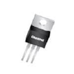
- 型号: MJE13005
- 制造商: Central Semiconductor
- 库位|库存: xxxx|xxxx
- 要求:
| 数量阶梯 | 香港交货 | 国内含税 |
| +xxxx | $xxxx | ¥xxxx |
查看当月历史价格
查看今年历史价格
MJE13005产品简介:
ICGOO电子元器件商城为您提供MJE13005由Central Semiconductor设计生产,在icgoo商城现货销售,并且可以通过原厂、代理商等渠道进行代购。 MJE13005价格参考。Central SemiconductorMJE13005封装/规格:晶体管 - 双极 (BJT) - 单, 双极 (BJT) 晶体管 NPN 400V 4A 4MHz 2W 通孔 TO-220AB。您可以下载MJE13005参考资料、Datasheet数据手册功能说明书,资料中有MJE13005 详细功能的应用电路图电压和使用方法及教程。
MJE13005是ON Semiconductor公司生产的单个双极晶体管(BJT),属于功率晶体管系列。该型号的晶体管具有高电流、高电压和低饱和压降的特点,适用于多种电力电子应用领域。以下是MJE13005的主要应用场景:

1. 开关电源(SMPS):MJE13005常用于开关电源中的功率级电路,如升压、降压或反激式转换器。其高电流处理能力和快速开关特性使其能够有效提高电源效率并减少热量损失。

2. 音频放大器:在音频设备中,MJE13005可以用作输出级晶体管,驱动扬声器或其他负载。其良好的线性度和低失真特性有助于提供高质量的声音输出。

3. 电机驱动:该晶体管适合用于小到中等功率的直流电机驱动电路,可以实现对电机的速度和方向进行精确控制。它能够承受较大的电流波动,确保电机运行稳定。

4. 继电器驱动:MJE13005可用于驱动电磁继电器,通过控制基极电流来切换大电流负载。它的高耐压性能保证了即使在恶劣环境下也能可靠工作。

5. 保护电路:在过流保护、短路保护等安全电路设计中,MJE13005可以作为关键元件之一,当检测到异常情况时迅速切断电路以防止损坏其他组件。

6. 工业自动化与控制:在PLC、传感器接口以及其他工业控制系统中,MJE13005可以用来放大信号或驱动执行机构,如阀门、泵等。

总之,MJE13005凭借其优异的电气参数和可靠性,在众多需要高效能、高性能的电子设备和系统中得到了广泛应用。
| 参数 | 数值 |
| 品牌 | Central Semiconductor |
| 产品目录 | 半导体 |
| 描述 | 两极晶体管 - BJT NPN Fast SW |
| 产品分类 | 分离式半导体 |
| 产品手册 | |
| 产品图片 |
|
| rohs | 符合RoHS |
| 产品系列 | 晶体管,两极晶体管 - BJT,Central Semiconductor MJE13005 |
| 产品型号 | MJE13005 |
| 产品种类 | 两极晶体管 - BJT |
| 发射极-基极电压VEBO | 9 V |
| 商标 | Central Semiconductor |
| 增益带宽产品fT | 4 MHz |
| 安装风格 | Through Hole |
| 封装 | Bulk |
| 封装/箱体 | TO-220 |
| 工厂包装数量 | 400 |
| 晶体管极性 | NPN |
| 最大功率耗散 | 2000 mW |
| 最大工作温度 | + 150 C |
| 最大直流电集电极电流 | 4 A |
| 最小工作温度 | - 65 C |
| 直流集电极/BaseGainhfeMin | 10 |
| 系列 | MJE13005 |
| 集电极—发射极最大电压VCEO | 400 V |


- 商务部:美国ITC正式对集成电路等产品启动337调查
- 曝三星4nm工艺存在良率问题 高通将骁龙8 Gen1或转产台积电
- 太阳诱电将投资9.5亿元在常州建新厂生产MLCC 预计2023年完工
- 英特尔发布欧洲新工厂建设计划 深化IDM 2.0 战略
- 台积电先进制程称霸业界 有大客户加持明年业绩稳了
- 达到5530亿美元!SIA预计今年全球半导体销售额将创下新高
- 英特尔拟将自动驾驶子公司Mobileye上市 估值或超500亿美元
- 三星加码芯片和SET,合并消费电子和移动部门,撤换高东真等 CEO
- 三星电子宣布重大人事变动 还合并消费电子和移动部门
- 海关总署:前11个月进口集成电路产品价值2.52万亿元 增长14.8%


.jpg)
PDF Datasheet 数据手册内容提取
DATA SHEET MJE13005 NPN SILICON POWER TRANSISTOR JEDEC TO-220 CASE DESCRIPTION The CENTRAL SEMICONDUCTOR MJE13005 is a Silicon NPN Power Transistor, designed for high speed power switching applications. MAXIMUM RATINGS (TC=25°C unless otherwise noted) SYMBOL UNITS Collector-Emitter Voltage VCEO 400 V Collector-Emitter Voltage VCEV 700 V Emitter-Base Voltage VEBO 9.0 V Collector Current IC 4.0 A Peak Collector Current ICM 8.0 A Base Current IB 2.0 A Peak Base Current IBM 4.0 A Emitter Current IE 6.0 A Peak Emitter Current IEM 12 A Power Dissipation (TA=25°C) PD 2.0 W Power Dissipation PD 75 W Operating and Storage Junction Temperature TJ,Tstg -65 to +150 °C Thermal Resistance ΘJA 62.5 °C/W Thermal Resistance ΘJC 1.67 °C/W ELECTRICAL CHARACTERISTICS (TC=25°C unless otherwise noted) SYMBOL TEST CONDITIONS MIN MAX UNITS ICEV VCE=700V, VBE(OFF)=1.5V 1.0 mA ICEV VCE=700V, VBE(OFF)=1.5V, TC=100°C 5.0 mA IEBO VEB=9.0V 1.0 mA BVCEO IC=10mA 400 V VCE(SAT) IC=1.0A, IB=0.2A 0.5 V VCE(SAT) IC=2.0A, IB=0.5A 0.6 V VCE(SAT) IC=4.0A, IB=1.0A 1.0 V VBE(SAT) IC=1.0A, IB=0.2A 1.2 V VBE(SAT) IC=2.0A, IB=0.5A 1.6 V hFE VCE=5.0V, IC=1.0A 10 60 hFE VCE=5.0V, IC=2.0A 8.0 40 (Continued) R1
MJE13005 NPN POWER TRANSISTOR ELECTRICAL CHARACTERISTICS (CONTINUED) SYMBOL TEST CONDITIONS MIN TYP MAX UNITS fT VCE=10V, IC=500mA, f=1.0MHz 4.0 MHz Cob VCB=10V, IE=0, f=100kHz 130 pF Resistive Load t V =125V, I =2.0A, I = I =0.4A 0.1 µs d CC C B1 B2 t t =25µs, Duty Cycle ≤ 1.0% 0.7 µs r p t 4.0 µs s t 0.9 µs f Inductive Load tsv IC=2.0A, Vclamp=300V, IB1=0.4A, 4.0 µs tc VBE(off)=5.0V, TC=100°C 0.9 µs tfi 0.16 µs TO-220 PACKAGE - MECHANICAL OUTLINE A E DIMENSIONS F INCHES MILLIMETERS SYMBOL MIN MAX MIN MAX B A 0.170 0.190 4.31 4.82 B 0.045 0.055 1.15 1.39 G C 0.013 0.026 0.33 0.65 H D 0.083 0.107 2.10 2.72 E 0.394 0.417 10.01 10.60 I F (DIA) 0.140 0.157 3.55 4.00 G 0.100 0.118 2.54 3.00 H 0.230 0.270 5.85 6.85 1 2 3 I 0.560 0.625 14.23 15.87 J - 0.250 - 6.35 J K 0.025 0.038 0.64 0.96 L 0.500 0.579 12.70 14.70 C L M 0.090 0.110 2.29 2.79 K TO-220 (REV: R2) D M Lead Code: R2 1) Base 2) Collector 3) Emitter Tab is Common to Pin 2
OUTSTANDING SUPPORT AND SUPERIOR SERVICES PRODUCT SUPPORT Central’s operations team provides the highest level of support to insure product is delivered on-time. • Supply management (Customer portals) • Custom bar coding for shipments • Inventory bonding • Custom product packing • Consolidated shipping options DESIGNER SUPPORT/SERVICES Central’s applications engineering team is ready to discuss your design challenges. Just ask. • Free quick ship samples (2nd day air) • Special wafer diffusions • Online technical data and parametric search • PbSn plating options • SPICE models • Package details • Custom electrical curves • Application notes • Environmental regulation compliance • Application and design sample kits • Customer specific screening • Custom product and package development • Up-screening capabilities REQUESTING PRODUCT PLATING 1. If requesting Tin/Lead plated devices, add the suffix “ TIN/LEAD” to the part number when ordering (example: 2N2222A TIN/LEAD). 2. If requesting Lead (Pb) Free plated devices, add the suffix “ PBFREE” to the part number when ordering (example: 2N2222A PBFREE). CONTACT US Corporate Headquarters & Customer Support Team Central Semiconductor Corp. 145 Adams Avenue Worldwide Field Representatives: Hauppauge, NY 11788 USA www.centralsemi.com/wwreps Main Tel: (631) 435-1110 Main Fax: (631) 435-1824 Worldwide Distributors: Support Team Fax: (631) 435-3388 www.centralsemi.com/wwdistributors www.centralsemi.com For the latest version of Central Semiconductor’s LIMITATIONS AND DAMAGES DISCLAIMER, which is part of Central’s Standard Terms and Conditions of sale, visit: www.centralsemi.com/terms www.centralsemi.com (001)
Mouser Electronics Authorized Distributor Click to View Pricing, Inventory, Delivery & Lifecycle Information: C entral Semiconductor: MJE13005 LEADFREE MJE13005