ICGOO在线商城 > 分立半导体产品 > 晶体管 - 双极 (BJT) - 单 > MJD340G

 Datasheet下载
- 型号: MJD340G
- 制造商: ON Semiconductor
- 库位|库存: xxxx|xxxx
- 要求:
| 数量阶梯 | 香港交货 | 国内含税 |
| +xxxx | $xxxx | ¥xxxx |
查看当月历史价格
查看今年历史价格
MJD340G产品简介:
ICGOO电子元器件商城为您提供MJD340G由ON Semiconductor设计生产,在icgoo商城现货销售,并且可以通过原厂、代理商等渠道进行代购。 MJD340G价格参考。ON SemiconductorMJD340G封装/规格:晶体管 - 双极 (BJT) - 单, 双极 (BJT) 晶体管 NPN 300V 500mA 10MHz 1.56W 表面贴装 DPAK。您可以下载MJD340G参考资料、Datasheet数据手册功能说明书,资料中有MJD340G 详细功能的应用电路图电压和使用方法及教程。
| 参数 | 数值 |
| 产品目录 | |
| 描述 | TRANS POWER NPN 0.5A 300V DPAK两极晶体管 - BJT 0.5A 300V 15W NPN |
| 产品分类 | 晶体管(BJT) - 单路分离式半导体 |
| 品牌 | ON Semiconductor |
| 产品手册 | |
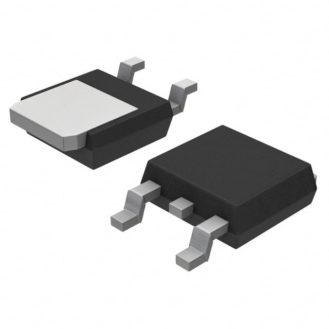
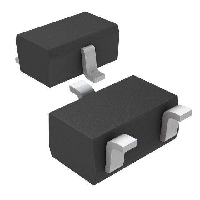
| 产品图片 |
|
| rohs | 符合RoHS无铅 / 符合限制有害物质指令(RoHS)规范要求 |
| 产品系列 | 晶体管,两极晶体管 - BJT,ON Semiconductor MJD340G- |
| 数据手册 | |
| 产品型号 | MJD340G |
| PCN组件/产地 | |
| 不同 Ib、Ic时的 Vce饱和值(最大值) | - |
| 不同 Ic、Vce 时的DC电流增益(hFE)(最小值) | 30 @ 50mA,10V |
| 产品目录页面 | |
| 产品种类 | 两极晶体管 - BJT |
| 供应商器件封装 | DPAK-3 |
| 其它名称 | MJD340G-ND |
| 功率-最大值 | 1.56W |
| 包装 | 管件 |
| 发射极-基极电压VEBO | 3 V |
| 商标 | ON Semiconductor |
| 安装类型 | 表面贴装 |
| 安装风格 | SMD/SMT |
| 封装 | Tube |
| 封装/外壳 | TO-252-3,DPak(2 引线+接片),SC-63 |
| 封装/箱体 | TO-252-3 (DPAK) |
| 工厂包装数量 | 75 |
| 晶体管极性 | NPN |
| 晶体管类型 | NPN |
| 最大功率耗散 | 15 W |
| 最大工作温度 | + 150 C |
| 最大直流电集电极电流 | 0.5 A |
| 最小工作温度 | - 65 C |
| 标准包装 | 75 |
| 电压-集射极击穿(最大值) | 300V |
| 电流-集电极(Ic)(最大值) | 500mA |
| 电流-集电极截止(最大值) | 100µA |
| 直流集电极/BaseGainhfeMin | 30 |
| 系列 | MJD340 |
| 配置 | Single |
| 集电极—发射极最大电压VCEO | 300 V |
| 集电极—基极电压VCBO | 300 V |
| 集电极—射极饱和电压 | 1 V |
| 集电极连续电流 | 0.5 A |
| 频率-跃迁 | - |


- 商务部:美国ITC正式对集成电路等产品启动337调查
- 曝三星4nm工艺存在良率问题 高通将骁龙8 Gen1或转产台积电
- 太阳诱电将投资9.5亿元在常州建新厂生产MLCC 预计2023年完工
- 英特尔发布欧洲新工厂建设计划 深化IDM 2.0 战略
- 台积电先进制程称霸业界 有大客户加持明年业绩稳了
- 达到5530亿美元!SIA预计今年全球半导体销售额将创下新高
- 英特尔拟将自动驾驶子公司Mobileye上市 估值或超500亿美元
- 三星加码芯片和SET,合并消费电子和移动部门,撤换高东真等 CEO
- 三星电子宣布重大人事变动 还合并消费电子和移动部门
- 海关总署:前11个月进口集成电路产品价值2.52万亿元 增长14.8%


PDF Datasheet 数据手册内容提取
MJD340(cid:2)(NPN), MJD350(cid:2)(PNP) High Voltage Power Transistors DPAK for Surface Mount Applications Designed for line operated audio output amplifier, switchmode www.onsemi.com power supply drivers and other switching applications. Features SILICON • Lead Formed for Surface Mount Applications in Plastic Sleeves POWER TRANSISTORS (No Suffix) 0.5 AMPERE • Electrically Similar to Popular MJE340 and MJE350 300 VOLTS, 15 WATTS • Epoxy Meets UL 94 V−0 @ 0.125 in • NJV Prefix for Automotive and Other Applications Requiring COLLECTOR COLLECTOR Unique Site and Control Change Requirements; AEC−Q101 2, 4 2, 4 Qualified and PPAP Capable • These Devices are Pb−Free, Halogen Free/BFR Free and are RoHS Compliant 1 1 BASE BASE MAXIMUM RATINGS 3 3 Rating Symbol Max Unit EMITTER EMITTER Collector−Emitter Voltage VCEO 300 Vdc Collector−Base Voltage VCB 300 Vdc 4 Emitter−Base Voltage VEB 3 Vdc 1 2 Collector Current − Continuous IC 0.5 Adc 3 Collector Current − Peak ICM 0.75 Adc DPAK CASE 369C Total Power Dissipation PD @ TC = 25°C 15 W STYLE 1 Derate above 25°C 0.12 W/°C MARKING DIAGRAM Total Power Dissipation (Note 1) PD @ TA = 25°C 1.56 W Derate above 25°C 0.012 W/°C Operating and Storage Junction TJ, Tstg −65 to +150 °C AYWW Temperature Range J3x0G ESD − Human Body Model HBM V MJD340 (NPN) 3B MJD350 (PNP) 2 A =Assembly Location ESD − Machine Model MM V Y =Year MJD340 (NPN) M4 WW =Work Week MJD350 (PNP) M4 J3x0 =Device Code Stresses exceeding those listed in the Maximum Ratings table may damage the x= 4 or 5 device. If any of these limits are exceeded, device functionality should not be G =Pb−Free Package assumed, damage may occur and reliability may be affected. 1. These ratings are applicable when surface mounted on the minimum pad sizes recommended. ORDERING INFORMATION See detailed ordering and shipping information in the package dimensions section on page 5 of this data sheet. © Semiconductor Components Industries, LLC, 2016 1 Publication Order Number: June, 2016 − Rev. 12 MJD340/D
MJD340 (NPN), MJD350 (PNP) THERMAL CHARACTERISTICS Characteristic Symbol Max Unit Thermal Resistance, Junction−to−Case R(cid:2)JC 8.33 °C/W Thermal Resistance, Junction−to−Ambient (Note 2) R(cid:2)JA 80 °C/W Leading Temperature for Soldering Purpose TL 260 °C 2. These ratings are applicable when surface mounted on the minimum pad sizes recommended. ÎÎÎÎÎÎÎÎÎÎÎÎÎÎÎÎÎÎÎÎÎÎÎÎÎÎÎÎÎÎÎÎÎ ÎÎÎÎELEÎÎCTÎÎRICÎÎAL CÎÎHAÎÎRAÎÎCTEÎÎRISÎÎTICÎÎS (TÎÎC = ÎÎ25(cid:2)CÎÎ unÎÎless ÎÎotheÎÎrwisÎÎÎe noÎÎted)ÎÎÎÎÎÎÎÎÎÎÎÎÎÎÎÎÎÎÎÎÎÎÎÎÎÎÎÎÎÎÎ ÎÎÎÎÎÎÎÎÎÎÎÎÎÎÎÎChÎÎaracÎÎterisÎÎticÎÎÎÎÎÎÎÎÎÎÎÎÎÎÎÎÎSyÎÎmboÎÎl ÎÎÎÎÎMÎÎin ÎÎÎÎÎÎÎMÎÎax ÎÎÎÎÎÎÎUnÎÎit ÎÎ ÎÎOÎÎFFÎÎ CHAÎÎRAÎÎCTEÎÎRISTÎÎICSÎÎÎÎÎÎÎÎÎÎÎÎÎÎÎÎÎÎÎÎÎÎÎÎÎÎÎÎÎÎÎÎÎÎÎÎÎÎÎÎÎÎÎÎÎÎÎÎÎÎÎÎÎÎÎÎ ÎÎCollÎectoÎr−EmÎitterÎ SusÎtainÎing VÎoltaÎge (NÎote Î3) ÎÎÎÎÎÎÎÎVCEÎO(suÎs) ÎÎÎÎÎÎÎÎÎÎÎÎÎVÎÎ ÎÎÎÎ(IÎÎC = 1ÎÎ mAÎÎ, IB =ÎÎ 0)ÎÎÎÎÎÎÎÎÎÎÎÎÎÎÎÎÎÎÎÎÎÎÎÎÎÎÎÎÎÎÎÎÎÎÎÎÎÎ3ÎÎ00 ÎÎÎÎÎÎÎÎ−ÎÎÎÎÎÎÎÎÎÎÎÎÎÎ ÎÎCollÎectoÎr CuÎtoff CÎurreÎnt ÎÎÎÎÎÎÎÎÎÎÎÎÎICÎEOÎÎÎÎÎÎÎÎÎÎÎÎÎÎmÎA Î (VCB = 300 V, IE = 0) − 0.1 ÎÎÎÎÎÎÎÎÎÎÎÎÎÎÎÎÎÎÎÎÎÎÎÎÎÎÎÎÎÎÎÎÎÎÎÎÎÎÎÎÎÎÎÎÎÎÎÎÎÎÎÎÎÎÎÎÎÎÎÎÎÎÎÎÎÎÎÎÎÎÎÎÎÎ Emitter Cutoff Current IEBO mA ÎÎÎÎ(VÎÎBE =ÎÎ 3 VÎÎ, IC =ÎÎ 0)ÎÎÎÎÎÎÎÎÎÎÎÎÎÎÎÎÎÎÎÎÎÎÎÎÎÎÎÎÎÎÎÎÎÎÎÎÎÎ− ÎÎÎÎÎÎÎ0ÎÎ.1 ÎÎÎÎÎÎÎÎÎÎÎ ÎÎOÎÎN CÎÎHAÎÎRACÎÎTERÎÎISTIÎÎCS ÎÎ(NoteÎÎ 3)ÎÎÎÎÎÎÎÎÎÎÎÎÎÎÎÎÎÎÎÎÎÎÎÎÎÎÎÎÎÎÎÎÎÎÎÎÎÎÎÎÎÎÎÎÎÎÎÎÎÎÎÎ ÎÎDC ÎCurrÎent GÎainÎÎÎÎÎÎÎÎÎÎÎÎÎÎÎhÎFE ÎÎÎÎÎÎÎÎÎÎÎÎÎÎ−ÎÎ ÎÎÎÎ(IÎÎC = 5ÎÎ0 mÎÎA, VÎÎCE =ÎÎ 10 VÎÎ) ÎÎÎÎÎÎÎÎÎÎÎÎÎÎÎÎÎÎÎÎÎÎÎÎÎÎÎÎÎÎÎÎÎÎ3ÎÎ0 ÎÎÎÎÎÎÎÎ24ÎÎ0 ÎÎÎÎÎÎÎÎÎÎÎÎ ÎÎCollÎectoÎr−EmÎitterÎ SatÎuratiÎon VÎoltagÎe ÎÎÎÎÎÎÎÎÎÎVCÎE(satÎ) ÎÎÎÎÎÎÎÎÎÎÎÎÎVÎÎ (IC = 100 mA, IB = 10 mA) − 1 ÎÎÎÎÎÎÎÎÎÎÎÎÎÎÎÎÎÎÎÎÎÎÎÎÎÎÎÎÎÎÎÎÎÎÎÎÎÎÎÎÎÎÎÎÎÎÎÎÎÎÎÎÎÎÎÎÎÎÎÎÎÎÎÎÎÎÎÎÎÎÎÎÎÎ Base−Emitter On Voltage VBE(on) V ÎÎÎÎ(IÎÎC = 1ÎÎ A, VÎÎCE ÎÎ= 10ÎÎ V) ÎÎÎÎÎÎÎÎÎÎÎÎÎÎÎÎÎÎÎÎÎÎÎÎÎÎÎÎÎÎÎÎÎÎÎÎ− ÎÎÎÎÎÎÎ1ÎÎ.5 ÎÎÎÎÎÎÎÎÎÎÎ ÎÎÎÎDYNÎÎAMIÎÎC CÎÎHARÎÎACTÎÎERIÎÎSTICÎÎS ÎÎÎÎÎÎÎÎÎÎÎÎÎÎÎÎÎÎÎÎÎÎÎÎÎÎÎÎÎÎÎÎÎÎÎÎÎÎÎÎÎÎÎÎÎÎÎÎÎÎÎÎ ÎÎCurrÎent ÎGainÎ − BÎandwÎidthÎ ProÎductÎÎÎÎÎÎÎÎÎÎÎÎfT ÎÎÎÎÎÎÎÎÎÎÎÎÎÎMHÎz Î (IC = 50 mA, VCE = 10 V, f = 10 MHz) 10 − ÎÎÎÎÎÎÎÎÎÎÎÎÎÎÎÎÎÎÎÎÎÎÎÎÎÎÎÎÎÎÎÎÎÎÎÎÎ Product parametric performance is indicated in the Electrical Characteristics for the listed test conditions, unless otherwise noted. Product performance may not be indicated by the Electrical Characteristics if operated under different conditions. 3. Pulse Test: Pulse Width ≤ 300 (cid:3)s, Duty Cycle ≤ 2%. www.onsemi.com 2
MJD340 (NPN), MJD350 (PNP) TYPICAL CHARACTERISTICS MJD340 300 200 VCE = 2 V VCE = 10 V AIN TJ = 150°C G 100 T REN 70 +100°C R U 50 C C +(cid:2)25°C D , E 30 F h 20 -(cid:2)55°C 10 1 2 3 5 7 10 20 30 50 70 100 200 300 500 IC, COLLECTOR CURRENT (mAdc) Figure 1. DC Current Gain MJD340 1 TJ = 25°C 0.8 VBE(sat) @ IC/IB = 10 S) T OL 0.6 VBE @ VCE = 10 V V E ( G A LT 0.4 O V V, VCE(sat) @ IC/IB = 10 0.2 IC/IB = 5 0 10 20 30 50 100 200 300 500 IC, COLLECTOR CURRENT (mA) Figure 2. “On” Voltages MJD350 MJD350 200 1 1 TJ = 150°C TJ = 25°C 100 25°C 0.8 N VBE(sat) @ IC/IB = 10 GAI 70 TS) RRENT 50 -(cid:2)55°C GE (VOL 0.6 VBE @ VCE = 10 V , DC CUE 30 V, VOLTA 0.4 IC/IB = 10 hF 20 VCE = 2 V 0.2 VCC = 10 V VCE(sat) IC/IB = 5 10 0 5 7 10 20 30 50 70 100 200 300 500 5 7 10 20 30 50 70 100 200 300 500 IC, COLLECTOR CURRENT (mA) IC, COLLECTOR CURRENT (mA) Figure 3. DC Current Gain Figure 4. “On” Voltages www.onsemi.com 3
MJD340 (NPN), MJD350 (PNP) 1 0.7 D = 0.5 0.5 HERMALMALIZED) 00..23 00..21 R(cid:2)JC(t) = r(t) R(cid:2)JC P(pk) NSIENT TNCE (NOR00.0.17 00..0015 RDPU (cid:2)CJLCUS R=E V 8TE.R3S3A °AICNP/ PWSLH YMO FAWOXNR POWER t1 r(t), TRARESISTA00..0053 SINGLE PULSE RTJE(pAkD) - T TIMC E= APT(p tk1) (cid:2)JC(t) DUTY CtY2CLE, D = t1/t2 0.02 0.01 0.01 0.02 0.03 0.05 0.1 0.2 0.3 0.5 1 2 3 5 10 20 30 50 100 200 300 500 1 k t, TIME (ms) Figure 5. Thermal Response 1000 There are two limitations on the power handling ability of 100 (cid:3)s 500 a transistor: average junction temperature and second A)230000 500 (cid:3)s breakdown. Safe operating area curves indicate IC − VCE m 1 ms limits of the transistor that must be observed for reliable NT (100 operation; i.e., the transistor must not be subjected to greater E RR 50 dissipation than the curves indicate. OR CU 2300 dc vaTrihabe lde adteap oefn dFiinggu roen 6c oisn dbiatisoends .o Sne TcoJ(npdk )b =re a1k5d0o(cid:2)wCn; TpuCl sies T C LE 10 limits are valid for duty cycles to 10% provided TJ(pk) COL 5 ≤ 150(cid:2)C. TJ(pk) may be calculated from the data in , C 3 Figure 5. At high case temperatures, thermal limitations will I 2 reduce the power that can be handled to values less than the 1 limitations imposed by second breakdown. 10 20 30 50 70 100 200 300 500 7001000 VCE, COLLECTOR-EMITTER VOLTAGE (VOLTS) Figure 6. Active Region Safe Operating Area TA TC 2.5 25 S) T 2 20 T A W N ( TIO 1.5 15 A SIP TA S DI 1 10 TC R E W O P 0.5 5 , D P 0 0 25 50 75 100 125 150 T, TEMPERATURE (°C) Figure 7. Power Derating www.onsemi.com 4
MJD340 (NPN), MJD350 (PNP) ORDERING INFORMATION Device Package Shipping† MJD340G DPAK 75 Units / Rail (Pb−Free) MJD340RLG DPAK 1,800 / Tape & Reel (Pb−Free) MJD340T4G DPAK 2,500 / Tape & Reel (Pb−Free) NJVMJD340T4G DPAK 2,500 / Tape & Reel (Pb−Free) MJD350G DPAK 75 Units / Rail (Pb−Free) MJD350T4G DPAK 2,500 / Tape & Reel (Pb−Free) NJVMJD350T4G DPAK 2,500 / Tape & Reel (Pb−Free) †For information on tape and reel specifications, including part orientation and tape sizes, please refer to our Tape and Reel Packaging Specifications Brochure, BRD8011/D. www.onsemi.com 5
MJD340 (NPN), MJD350 (PNP) PACKAGE DIMENSIONS DPAK (SINGLE GAUGE) CASE 369C ISSUE F NOTES: A 1.DIMENSIONING AND TOLERANCING PER ASME Y14.5M, 1994. E C 2.CONTROLLING DIMENSION: INCHES. A 3.THERMAL PAD CONTOUR OPTIONAL WITHIN DI- b3 B MENSIONS b3, L3 and Z. c2 4.DIMENSIONS D AND E DO NOT INCLUDE MOLD FLASH, PROTRUSIONS, OR BURRS. MOLD FLASH, PROTRUSIONS, OR GATE BURRS SHALL 4 NOT EXCEED 0.006 INCHES PER SIDE. L3 Z 5.DIMENSIONS D AND E ARE DETERMINED AT THE D DETAIL A H 6.DOAUTTUEMRSM OA SATN EDX BT RAERME EDSE OTEFR TMHIEN EPDLA ASTT DICA TBUOMDY. 1 2 3 PLANE H. 7.OPTIONAL MOLD FEATURE. L4 INCHES MILLIMETERS NOTE 7 b2 c BOTTOM VIEW DIM MIN MAX MIN MAX A 0.086 0.094 2.18 2.38 e SIDE VIEW A1 0.000 0.005 0.00 0.13 b b 0.025 0.035 0.63 0.89 0.005 (0.13) M C b2 0.028 0.045 0.72 1.14 TOP VIEW b3 0.180 0.215 4.57 5.46 c 0.018 0.024 0.46 0.61 c2 0.018 0.024 0.46 0.61 H Z Z D 0.235 0.245 5.97 6.22 E 0.250 0.265 6.35 6.73 e 0.090 BSC 2.29 BSC L2 GPLAAUNGEE C SPELAATNIENG H 0.370 0.410 9.40 10.41 L 0.055 0.070 1.40 1.78 L1 0.114 REF 2.90 REF L2 0.020 BSC 0.51 BSC L A1 BOTTOM VIEW L3 0.035 0.050 0.89 1.27 L1 ALTERNATE L4 −−− 0.040 −−− 1.01 CONSTRUCTIONS Z 0.155 −−− 3.93 −−− DETAIL A ROTATED 90(cid:2) CW STYLE 1: PIN 1.BASE SOLDERING FOOTPRINT* 2.COLLECTOR 3.EMITTER 4.COLLECTOR 6.20 3.00 0.244 0.118 2.58 0.102 5.80 1.60 6.17 0.228 0.063 0.243 (cid:2) (cid:3) mm SCALE 3:1 inches *For additional information on our Pb−Free strategy and soldering details, please download the ON Semiconductor Soldering and Mounting Techniques Reference Manual, SOLDERRM/D. ON Semiconductor and are trademarks of Semiconductor Components Industries, LLC dba ON Semiconductor or its subsidiaries in the United States and/or other countries. ON Semiconductor owns the rights to a number of patents, trademarks, copyrights, trade secrets, and other intellectual property. A listing of ON Semiconductor’s product/patent coverage may be accessed at www.onsemi.com/site/pdf/Patent−Marking.pdf. ON Semiconductor reserves the right to make changes without further notice to any products herein. ON Semiconductor makes no warranty, representation or guarantee regarding the suitability of its products for any particular purpose, nor does ON Semiconductor assume any liability arising out of the application or use of any product or circuit, and specifically disclaims any and all liability, including without limitation special, consequential or incidental damages. Buyer is responsible for its products and applications using ON Semiconductor products, including compliance with all laws, regulations and safety requirements or standards, regardless of any support or applications information provided by ON Semiconductor. “Typical” parameters which may be provided in ON Semiconductor data sheets and/or specifications can and do vary in different applications and actual performance may vary over time. All operating parameters, including “Typicals” must be validated for each customer application by customer’s technical experts. ON Semiconductor does not convey any license under its patent rights nor the rights of others. ON Semiconductor products are not designed, intended, or authorized for use as a critical component in life support systems or any FDA Class 3 medical devices or medical devices with a same or similar classification in a foreign jurisdiction or any devices intended for implantation in the human body. Should Buyer purchase or use ON Semiconductor products for any such unintended or unauthorized application, Buyer shall indemnify and hold ON Semiconductor and its officers, employees, subsidiaries, affiliates, and distributors harmless against all claims, costs, damages, and expenses, and reasonable attorney fees arising out of, directly or indirectly, any claim of personal injury or death associated with such unintended or unauthorized use, even if such claim alleges that ON Semiconductor was negligent regarding the design or manufacture of the part. ON Semiconductor is an Equal Opportunity/Affirmative Action Employer. This literature is subject to all applicable copyright laws and is not for resale in any manner. PUBLICATION ORDERING INFORMATION LITERATURE FULFILLMENT: N. American Technical Support: 800−282−9855 Toll Free ON Semiconductor Website: www.onsemi.com Literature Distribution Center for ON Semiconductor USA/Canada 19521 E. 32nd Pkwy, Aurora, Colorado 80011 USA Europe, Middle East and Africa Technical Support: Order Literature: http://www.onsemi.com/orderlit Phone: 303−675−2175 or 800−344−3860 Toll Free USA/Canada Phone: 421 33 790 2910 Fax: 303−675−2176 or 800−344−3867 Toll Free USA/Canada Japan Customer Focus Center For additional information, please contact your local Email: orderlit@onsemi.com Phone: 81−3−5817−1050 Sales Representative www.onsemi.com MJD340/D 6
Mouser Electronics Authorized Distributor Click to View Pricing, Inventory, Delivery & Lifecycle Information: O N Semiconductor: MJD340G MJD340RLG MJD340T4G MJD350T4G NJVMJD340T4G NJVMJD350T4G