ICGOO在线商城 > 分立半导体产品 > 晶体管 - 双极 (BJT) - 单 > MJD200T4G
 Datasheet下载
- 型号: MJD200T4G
- 制造商: ON Semiconductor
- 库位|库存: xxxx|xxxx
- 要求:
| 数量阶梯 | 香港交货 | 国内含税 |
| +xxxx | $xxxx | ¥xxxx |
查看当月历史价格
查看今年历史价格
MJD200T4G产品简介:
ICGOO电子元器件商城为您提供MJD200T4G由ON Semiconductor设计生产,在icgoo商城现货销售,并且可以通过原厂、代理商等渠道进行代购。 MJD200T4G价格参考。ON SemiconductorMJD200T4G封装/规格:晶体管 - 双极 (BJT) - 单, Bipolar (BJT) Transistor NPN 25V 5A 65MHz 1.4W Surface Mount DPAK。您可以下载MJD200T4G参考资料、Datasheet数据手册功能说明书,资料中有MJD200T4G 详细功能的应用电路图电压和使用方法及教程。
ON Semiconductor(安森美)的MJD200T4G是一款NPN型双极结型晶体管(BJT),属于功率晶体管类别,常用于中高电流、高电压开关与放大应用。其主要应用场景包括:

1. 电源管理电路:适用于线性稳压器、开关电源(SMPS)中的驱动级或控制电路,因其具备较高的耐压(VCEO达100V)和大电流承载能力(Ic可达5A),适合处理较大功率负载。

2. 电机驱动:广泛应用于工业控制、家用电器(如风扇、洗衣机)中的直流电机或步进电机驱动电路,作为开关元件控制电机启停与转速。

3. 照明系统:可用于LED驱动电路,特别是需要大电流控制的场合,如汽车照明、工业照明等,实现高效开关控制。

4. 继电器与电磁阀驱动:在自动化控制系统中,MJD200T4G常用于驱动继电器、电磁阀等电感性负载,具备良好的饱和导通特性,降低功耗。

5. 逆变器与转换器:在DC-AC逆变器、DC-DC转换器中作为功率开关使用,适用于太阳能逆变器、UPS不间断电源等设备。

6. 汽车电子:由于其符合AEC-Q101车规标准,MJD200T4G也广泛用于汽车电子系统,如车身控制模块、灯光控制、电动门窗等。

该器件采用TO-252(D-Pak)封装,便于散热和表面贴装,适合紧凑型高功率密度设计。总体而言,MJD200T4G适用于需要高可靠性、高效率和中等功率切换的各种工业、消费及汽车类应用。
| 参数 | 数值 |
| 产品目录 | |
| 描述 | TRANS PWR NPN 5A 25V DPAK两极晶体管 - BJT 5A 25V 12.5W NPN |
| 产品分类 | 晶体管(BJT) - 单路分离式半导体 |
| 品牌 | ON Semiconductor |
| 产品手册 | |
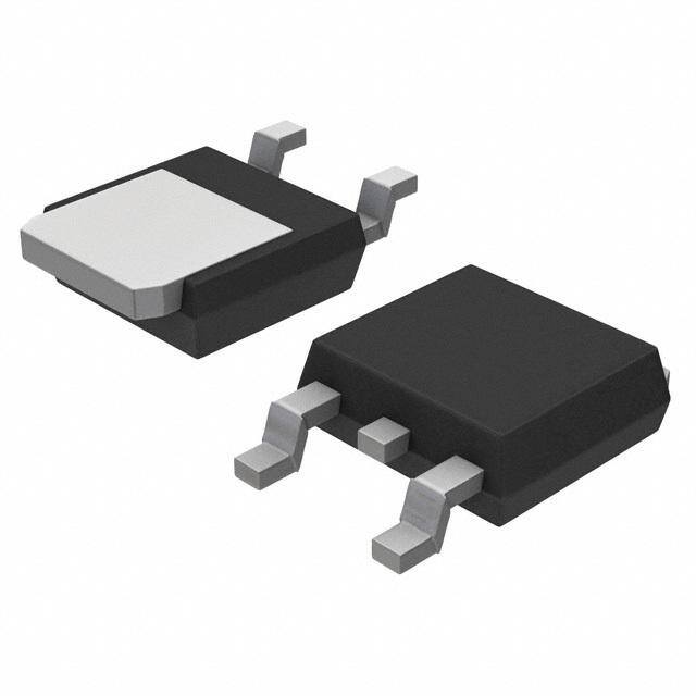
| 产品图片 |
|
| rohs | 符合RoHS无铅 / 符合限制有害物质指令(RoHS)规范要求 |
| 产品系列 | 晶体管,两极晶体管 - BJT,ON Semiconductor MJD200T4G- |
| 数据手册 | |
| 产品型号 | MJD200T4G |
| PCN组件/产地 | |
| 不同 Ib、Ic时的 Vce饱和值(最大值) | 1.8V @ 1A,5A |
| 不同 Ic、Vce 时的DC电流增益(hFE)(最小值) | 45 @ 2A,1V |
| 产品目录页面 | |
| 产品种类 | 两极晶体管 - BJT |
| 供应商器件封装 | DPAK-3 |
| 其它名称 | MJD200T4GOSDKR |
| 功率-最大值 | 1.4W |
| 包装 | Digi-Reel® |
| 发射极-基极电压VEBO | 8 V |
| 商标 | ON Semiconductor |
| 增益带宽产品fT | 65 MHz |
| 安装类型 | 表面贴装 |
| 安装风格 | SMD/SMT |
| 封装 | Reel |
| 封装/外壳 | TO-252-3,DPak(2 引线+接片),SC-63 |
| 封装/箱体 | TO-252-3 (DPAK) |
| 工厂包装数量 | 2500 |
| 晶体管极性 | NPN |
| 晶体管类型 | NPN |
| 最大功率耗散 | 12.5 W |
| 最大工作温度 | + 150 C |
| 最大直流电集电极电流 | 5 A |
| 最小工作温度 | - 65 C |
| 标准包装 | 1 |
| 电压-集射极击穿(最大值) | 25V |
| 电流-集电极(Ic)(最大值) | 5A |
| 电流-集电极截止(最大值) | - |
| 直流集电极/BaseGainhfeMin | 70 |
| 系列 | MJD200 |
| 配置 | Single |
| 集电极—发射极最大电压VCEO | 25 V |
| 集电极—基极电压VCBO | 40 V |
| 集电极—射极饱和电压 | 1.8 V |
| 集电极连续电流 | 5 A |
| 频率-跃迁 | 65MHz |


- 商务部:美国ITC正式对集成电路等产品启动337调查
- 曝三星4nm工艺存在良率问题 高通将骁龙8 Gen1或转产台积电
- 太阳诱电将投资9.5亿元在常州建新厂生产MLCC 预计2023年完工
- 英特尔发布欧洲新工厂建设计划 深化IDM 2.0 战略
- 台积电先进制程称霸业界 有大客户加持明年业绩稳了
- 达到5530亿美元!SIA预计今年全球半导体销售额将创下新高
- 英特尔拟将自动驾驶子公司Mobileye上市 估值或超500亿美元
- 三星加码芯片和SET,合并消费电子和移动部门,撤换高东真等 CEO
- 三星电子宣布重大人事变动 还合并消费电子和移动部门
- 海关总署:前11个月进口集成电路产品价值2.52万亿元 增长14.8%


PDF Datasheet 数据手册内容提取
MJD200 (NPN), MJD210 (PNP) Complementary Plastic Power Transistors NPN/PNP Silicon DPAK For Surface Mount Applications http://onsemi.com Designed for low voltage, low−power, high−gain audio SILICON amplifier applications. POWER TRANSISTORS Features 5 AMPERES • High DC Current Gain 25 VOLTS, 12.5 WATTS • Lead Formed for Surface Mount Applications in Plastic Sleeves (No Suffix) PNP NPN • Low Collector−Emitter Saturation Voltage COLLECTOR COLLECTOR • High Current−Gain − Bandwidth Product 2,4 2,4 • Annular Construction for Low Leakage • Epoxy Meets UL 94 V−0 @ 0.125 in 1 • 1 NJV Prefix for Automotive and Other Applications Requiring BASE BASE Unique Site and Control Change Requirements; AEC−Q101 Qualified and PPAP Capable 3 3 • These Devices are Pb−Free and are RoHS Compliant EMITTER EMITTER MAXIMUM RATINGS 4 Rating Symbol Max Unit 1 2 Collector−Base Voltage VCB 40 Vdc 3 Collector−Emitter Voltage VCEO 25 Vdc DPAK CASE 369C Emitter−Base Voltage VEB 8.0 Vdc STYLE 1 Collector Current − Continuous IC 5.0 Adc Collector Current − Peak ICM 10 Adc MARKING DIAGRAM Base Current IB 1.0 Adc Total Power Dissipation PD @De rTaCte = a 2b5o°vCe 25°C 102.1.5 WW/°C AYWW J2x0G Total Power Dissipation (Note 1) PD @ TA = 25°C 1.4 W Derate above 25°C 0.011 W/°C Operating and Storage Junction TJ, Tstg −65 to +150 °C A = Assembly Location Temperature Range Y =Year WW =Work Week ESD − Human Body Model HBM 3B V x = 1 or 0 ESD − Machine Model MM C V G =Pb−Free Package Stresses exceeding Maximum Ratings may damage the device. Maximum Ratings are stress ratings only. Functional operation above the Recommended Operating Conditions is not implied. Extended exposure to stresses above the ORDERING INFORMATION Recommended Operating Conditions may affect device reliability. See detailed ordering and shipping information in the package 1. These ratings are applicable when surface mounted on the minimum pad dimensions section on page 6 of this data sheet. sizes recommended. © Semiconductor Components Industries, LLC, 2013 1 Publication Order Number: September, 2013 − Rev. 13 MJD200/D
MJD200 (NPN), MJD210 (PNP) THERMAL CHARACTERISTICS Characteristic Symbol Max Unit Thermal Resistance, Junction−to−Case R(cid:2)JC 10 °C/W Thermal Resistance, Junction−to−Ambient (Note 2) R(cid:2)JA 89.3 °C/W 2. These ratings are applicable when surface mounted on the minimum pad sizes recommended. ELECTRICAL CHARACTERISTICS (TC = 25°C unless otherwise noted) Characteristic Symbol Min Max Unit OFF CHARACTERISTICS Collector−Emitter Sustaining Voltage (Note 3) VCEO(sus) Vdc (IC = 10 mAdc, IB = 0) 25 − Collector Cutoff Current VCBO (VCB = 40 Vdc, IE = 0) − 100 nAdc (VCB = 40 Vdc, IE = 0, TJ = 125°C) − 100 (cid:3)Adc Emitter Cutoff Current VEBO nAdc (VBE = 8 Vdc, IC = 0) − 100 ON CHARACTERISTICS C Current Gain (Note 3), hFE − (IC = 500 mAdc, VCE = 1 Vdc) 70 − (IC = 2 Adc, VCE = 1 Vdc) 45 180 (IC = 5 Adc, VCE = 2 Vdc) 10 − Collector−Emitter Saturation Voltage (Note 3) VCE(sat) Vdc (IC = 500 mAdc, IB = 50 mAdc) − 0.3 (IC = 2 Adc, IB = 200 mAdc) − 0.75 (IC = 5 Adc, IB = 1 Adc) − 1.8 Base−Emitter Saturation Voltage (Note 3) VBE(sat) Vdc (IC = 5 Adc, IB = 1 Adc) − 2.5 Base−Emitter On Voltage (Note 3) VBE(on) Vdc (IC = 2 Adc, VCE = 1 Vdc) − 1.6 DYNAMIC CHARACTERISTICS Current−Gain − Bandwidth Product (Note 4) fT MHz (IC = 100 mAdc, VCE = 10 Vdc, ftest = 10 MHz) 65 − Output Capacitance Cob pF (VCB = 10 Vdc, IE = 0, f = 0.1 MHz) MJD200 − 80 MJD210, NJVMJD210T4G − 120 3. Pulse Test: Pulse Width = 300 (cid:3)s, Duty Cycle (cid:2) 2%. 4. fT = ⎪hfe⎪• ftest. http://onsemi.com 2
MJD200 (NPN), MJD210 (PNP) TA TC 2.5 25 VCC +(cid:2)30 V TS) 2 20 25 (cid:3)s T WA +11 V RC N ( 0 SCOPE TIO1.5 15 RB A P -(cid:2)9 V SI R DIS 1 10 TA (SURFACE MOUNT) tr, tf ≤ 10 ns 51 D1 E DUTY CYCLE = 1% OW TC -(cid:2)4 V P0.5 5 P, D RB and RC VARIED TO OBTAIN DESIRED CURRENT LEVELS D1 MUST BE FAST RECOVERY TYPE, e.g.: 0 025 50 75 100 125 150 (cid:3)(cid:3)M1NS5D862150 U0 SUESDE DA BBOEVLEO WIB ≈IB 1≈0 100 m0A mA RFEOVRER PSNEP A TLELS PTO CLIARRCIUTIITE,S T, TEMPERATURE (°C) Figure 1. Power Derating Figure 2. Switching Time Test Circuit 1K 10K 500 td 5K VCC = 30 V 300 3K ts IC/IB = 10 200 2K IB1 = IB2 100 1K TJ = 25°C t, TIME (ns) 532000 tr IVCC/ICB == 3100 V t, TIME (ns) 532000000 10 TJ = 25°C 100 5 50 3 30 2 MJD200 20 MJD200 tf MJD210 MJD210 1 10 0.01 0.020.030.05 0.1 0.2 0.3 0.5 1 2 3 5 10 0.01 0.020.030.05 0.1 0.2 0.3 0.5 1 2 3 5 10 IC, COLLECTOR CURRENT (A) IC, COLLECTOR CURRENT (A) Figure 3. Turn−On Time Figure 4. Turn−Off Time http://onsemi.com 3
MJD200 (NPN), MJD210 (PNP) NPN PNP MJD200 MJD210 400 400 TJ = 150°C 25°C TJ = 150°C N 200 N 200 AI AI NT G -(cid:2)55°C NT G 25°C E E R 100 R 100 R R CU 80 CU 80 -(cid:2)55°C C C D 60 D 60 , E , E F F h 40 VCE = 1 V h 40 VCE = 1 V VCE = 2 V VCE = 2 V 20 20 0.050.07 0.1 0.2 0.3 0.5 0.7 1 2 3 5 0.050.070.1 0.2 0.3 0.5 0.7 1 2 3 5 IC, COLLECTOR CURRENT (A) IC, COLLECTOR CURRENT (A) Figure 5. DC Current Gain 2 2 TJ = 25°C TJ = 25°C 1.6 1.6 S) S) T T L L O 1.2 O 1.2 V V E ( E ( G G LTA 0.8 VBE(sat) @ IC/IB = 10 LTA 0.8 VBE(sat) @ IC/IB = 10 O O V V V, VBE @ VCE = 1 V V, VBE @ VCE = 1 V 0.4 0.4 VCE(sat) @ IC/IB = 10 VCE(sat) @ IC/IB = 10 0 0 0.050.07 0.1 0.2 0.3 0.5 0.7 1 2 3 5 0.05 0.07 0.1 0.2 0.3 0.5 0.7 1 2 3 5 IC, COLLECTOR CURRENT (A) IC, COLLECTOR CURRENT (A) Figure 6. “On” Voltage +(cid:2)2.5 +(cid:2)2.5 °V/C) +(cid:2)2 *APPLIES FOR IC/IB ≤ hFE/3 °V/C) +(cid:2)2 *APPLIES FOR IC/IB ≤ hFE/3 m m S (+(cid:2)1.5 S (+(cid:2)1.5 25°C to 150°C T T N +(cid:2)1 N +(cid:2)1 E E CI CI EFFI+(cid:2)0.5 (cid:2)VC for VCE(sat) 25°C to 150°C EFFI+(cid:2)0.5 *(cid:2)VC for VCE(sat) CO 0 CO 0 -(cid:2)55°C to 25°C RE -(cid:2)0.5 -(cid:2)55°C to 25°C RE -(cid:2)0.5 TU TU 25°C to 150°C RA -(cid:2)1 25°C to 150°C RA -(cid:2)1 EMPE-(cid:2)1.5 (cid:2)VB for VBE EMPE-(cid:2)1.5 (cid:2)VB for VBE -(cid:2)55°C to 25°C , TV -(cid:2)2 -(cid:2)55°C to 25°C , TV -(cid:2)2 θ θ -(cid:2)2.5 -(cid:2)2.5 0.05 0.07 0.1 0.2 0.3 0.5 0.7 1 2 3 5 0.05 0.07 0.1 0.2 0.3 0.5 0.7 1 2 3 5 IC, COLLECTOR CURRENT (A) IC, COLLECTOR CURRENT (A) Figure 7. Temperature Coefficients http://onsemi.com 4
MJD200 (NPN), MJD210 (PNP) 1 0.7 D = 0.5 0.5 THERMALRMALIZED) 00..23 00..21 R(cid:2)JC(t) = r(t) (cid:2)JC P(pk) r(t), TRANSIENT RESISTANCE (NO0000...000.1573 0.005 (SINGLE0 .P0U1LSE0.)02 RDPRTJU E(cid:2)C(JpLACUkSD) R=E- T V 1TTIEM0CRS° EAC= A I /ANPWPT( PpS MtkL1H)Y A(cid:2)O XFJWCO(NtR) POWER DUTtY1 CtY2CLE, D = t1/t2 0.02 0.01 0.02 0.05 0.1 0.2 0.5 1 2 5 10 20 50 100 200 t, TIME (ms) Figure 8. Thermal Response 10 There are two limitations on the power handling ability of 5(cid:4)ms 5 a transistor: average junction temperature and second NT (AMP) 213 TJ = 150°C 510000(cid:4)(cid:3)(cid:4)(cid:3)ss 1(cid:4)ms bloirpmeeairtkasdt iooofwn ;tn hi..e eS .t,a rtafhene s otirspateonrrsa itstihtnoagrt mamrueusast t nc buoert v boeebs ssiuenbrdvjieeccdat etfedo IrtoC r ge−lr ieVaabCtelEer E R R dissipation than the curves indicate. U dc R C The data of Figure 9 is based on TJ(pk) = 150°C; TC is TO BONDING WIRE LIMITED variable depending on conditions. Second breakdown pulse EC0.1 THERMALLY LIMITED @ TC = 25°C limits are valid for duty cycles to 10% provided T L J(pk) OL (cid:3)(SINGLE PULSE) ≤ 150°C. T may be calculated from the data in Figure 8. C SECOND BREAKDOWN LIMITED J(pk) I, C (cid:3)CURVES APPLY BELOW At high case temperatures, thermal limitations will reduce (cid:3)RATED VCEO the power that can be handled to values less than the 0.01 limitations imposed by second breakdown. 0.3 1 2 3 5 7 10 20 30 VCE, COLLECTOR−EMITTER VOLTAGE (V) Figure 9. Active Region Safe Operating Area 200 TJ = 25°C F) 100 Cib p E ( C N 70 A T CI A P 50 A C, C Cob MJD200 (NPN) 30 MJD210 (PNP) 20 0.4 0.6 1 2 4 6 10 20 40 VR, REVERSE VOLTAGE (V) Figure 10. Capacitance http://onsemi.com 5
MJD200 (NPN), MJD210 (PNP) ORDERING INFORMATION Device Package Type Shipping† MJD200G DPAK 75 Units / Rail (Pb−Free) MJD200RLG DPAK 1,800 / Tape & Reel (Pb−Free) MJD200T4G DPAK 2,500 / Tape & Reel (Pb−Free) MJD210G DPAK 75 Units / Rail (Pb−Free) MJD210RLG DPAK 1,800 / Tape & Reel (Pb−Free) MJD210T4G DPAK 2,500 / Tape & Reel (Pb−Free) NJVMJD210T4G* DPAK 2,500 / Tape & Reel (Pb−Free) †For information on tape and reel specifications, including part orientation and tape sizes, please refer to our Tape and Reel Packaging Specifications Brochure, BRD8011/D. *NJV Prefix for Automotive and Other Applications Requiring Unique Site and Control Change Requirements; AEC−Q101 Qualified and PPAP Capable http://onsemi.com 6
MJD200 (NPN), MJD210 (PNP) PACKAGE DIMENSIONS DPAK CASE 369C ISSUE D NOTES: C 1.DIMENSIONING AND TOLERANCING PER ASME A Y14.5M, 1994. E A 2.CONTROLLING DIMENSION: INCHES. 3.THERMAL PAD CONTOUR OPTIONAL WITHIN DI- MENSIONS b3, L3 and Z. b3 B c2 4.DIMENSIONS D AND E DO NOT INCLUDE MOLD FLASH, PROTRUSIONS, OR BURRS. MOLD FLASH, PROTRUSIONS, OR GATE BURRS SHALL NOT EXCEED 0.006 INCHES PER SIDE. L3 4 D Z 5.DOIUMTEENRSMIOONSST DE XATNRDE ME EASR EO FD ETTHEER PMLIANSETDIC A TB OTHDEY. H 6.DATUMS A AND B ARE DETERMINED AT DATUM 1 2 3 DETAIL A PLANE H. INCHES MILLIMETERS DIM MIN MAX MIN MAX L4 A 0.086 0.094 2.18 2.38 b2 A1 0.000 0.005 0.00 0.13 b c b 0.025 0.035 0.63 0.89 b2 0.030 0.045 0.76 1.14 e 0.005 (0.13) M C H b3 0.180 0.215 4.57 5.46 c 0.018 0.024 0.46 0.61 L2 GPLAAUNGEE C SPELAATNIENG cD2 00..203158 00..204254 50..9476 60..2621 E 0.250 0.265 6.35 6.73 e 0.090 BSC 2.29 BSC H 0.370 0.410 9.40 10.41 L A1 L 0.055 0.070 1.40 1.78 L1 L1 0.108 REF 2.74 REF L2 0.020 BSC 0.51 BSC DETAIL A L3 0.035 0.050 0.89 1.27 ROTATED 90(cid:2) CW L4 −−− 0.040 −−− 1.01 Z 0.155 −−− 3.93 −−− SOLDERING FOOTPRINT* STYLE 1: PIN 1.BASE 2.COLLECTOR 3.EMITTER 6.20 3.0 4.COLLECTOR 0.244 0.118 2.58 0.101 5.80 1.6 6.172 0.228 0.063 0.243 (cid:3) (cid:4) mm SCALE 3:1 inches *For additional information on our Pb−Free strategy and soldering details, please download the ON Semiconductor Soldering and Mounting Techniques Reference Manual, SOLDERRM/D. ON Semiconductor and are registered trademarks of Semiconductor Components Industries, LLC (SCILLC). SCILLC owns the rights to a number of patents, trademarks, copyrights, trade secrets, and other intellectual property. A listing of SCILLC’s product/patent coverage may be accessed at www.onsemi.com/site/pdf/Patent−Marking.pdf. SCILLC reserves the right to make changes without further notice to any products herein. SCILLC makes no warranty, representation or guarantee regarding the suitability of its products for any particular purpose, nor does SCILLC assume any liability arising out of the application or use of any product or circuit, and specifically disclaims any and all liability, including without limitation special, consequential or incidental damages. “Typical” parameters which may be provided in SCILLC data sheets and/or specifications can and do vary in different applications and actual performance may vary over time. All operating parameters, including “Typicals” must be validated for each customer application by customer’s technical experts. SCILLC does not convey any license under its patent rights nor the rights of others. SCILLC products are not designed, intended, or authorized for use as components in systems intended for surgical implant into the body, or other applications intended to support or sustain life, or for any other application in which the failure of the SCILLC product could create a situation where personal injury or death may occur. Should Buyer purchase or use SCILLC products for any such unintended or unauthorized application, Buyer shall indemnify and hold SCILLC and its officers, employees, subsidiaries, affiliates, and distributors harmless against all claims, costs, damages, and expenses, and reasonable attorney fees arising out of, directly or indirectly, any claim of personal injury or death associated with such unintended or unauthorized use, even if such claim alleges that SCILLC was negligent regarding the design or manufacture of the part. SCILLC is an Equal Opportunity/Affirmative Action Employer. This literature is subject to all applicable copyright laws and is not for resale in any manner. PUBLICATION ORDERING INFORMATION LITERATURE FULFILLMENT: N. American Technical Support: 800−282−9855 Toll Free ON Semiconductor Website: www.onsemi.com Literature Distribution Center for ON Semiconductor USA/Canada P.O. Box 5163, Denver, Colorado 80217 USA Europe, Middle East and Africa Technical Support: Order Literature: http://www.onsemi.com/orderlit Phone: 303−675−2175 or 800−344−3860 Toll Free USA/Canada Phone: 421 33 790 2910 Fax: 303−675−2176 or 800−344−3867 Toll Free USA/Canada Japan Customer Focus Center For additional information, please contact your local Email: orderlit@onsemi.com Phone: 81−3−5817−1050 Sales Representative http://onsemi.com MJD200/D 7
Mouser Electronics Authorized Distributor Click to View Pricing, Inventory, Delivery & Lifecycle Information: O N Semiconductor: MJD200G MJD200RLG MJD200T4G MJD210G MJD210RLG MJD210T4G