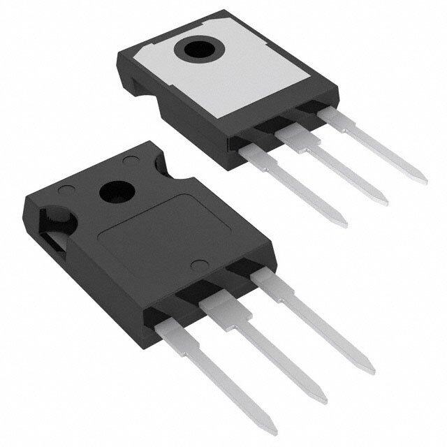
ICGOO在线商城 > 分立半导体产品 > 晶体管 - 双极 (BJT) - 单 > MJ14002G
- 型号: MJ14002G
- 制造商: ON Semiconductor
- 库位|库存: xxxx|xxxx
- 要求:
| 数量阶梯 | 香港交货 | 国内含税 |
| +xxxx | $xxxx | ¥xxxx |
查看当月历史价格
查看今年历史价格
MJ14002G产品简介:
ICGOO电子元器件商城为您提供MJ14002G由ON Semiconductor设计生产,在icgoo商城现货销售,并且可以通过原厂、代理商等渠道进行代购。 MJ14002G价格参考¥78.27-¥78.27。ON SemiconductorMJ14002G封装/规格:晶体管 - 双极 (BJT) - 单, 双极 (BJT) 晶体管 NPN 80V 60A 300W 通孔 TO-3。您可以下载MJ14002G参考资料、Datasheet数据手册功能说明书,资料中有MJ14002G 详细功能的应用电路图电压和使用方法及教程。
| 参数 | 数值 |
| 产品目录 | |
| 描述 | TRANS PWR NPN 60A 80V TO3两极晶体管 - BJT 60A 80V 300W NPN |
| 产品分类 | 晶体管(BJT) - 单路分离式半导体 |
| 品牌 | ON Semiconductor |
| 产品手册 | |
| 产品图片 |
|
| rohs | 符合RoHS无铅 / 符合限制有害物质指令(RoHS)规范要求 |
| 产品系列 | 晶体管,两极晶体管 - BJT,ON Semiconductor MJ14002G- |
| 数据手册 | |
| 产品型号 | MJ14002G |
| 不同 Ib、Ic时的 Vce饱和值(最大值) | 3V @ 12A,60A |
| 不同 Ic、Vce 时的DC电流增益(hFE)(最小值) | 15 @ 50A,3V |
| 产品目录页面 | |
| 产品种类 | 两极晶体管 - BJT |
| 供应商器件封装 | TO-3 |
| 其它名称 | MJ14002GOS |
| 功率-最大值 | 300W |
| 包装 | 托盘 |
| 发射极-基极电压VEBO | 5 V |
| 商标 | ON Semiconductor |
| 安装类型 | 通孔 |
| 安装风格 | SMD/SMT |
| 封装 | Tray |
| 封装/外壳 | TO-204AE |
| 封装/箱体 | SO EIAJ |
| 工厂包装数量 | 100 |
| 晶体管极性 | NPN |
| 晶体管类型 | NPN |
| 最大功率耗散 | 300 W |
| 最大工作温度 | + 150 C |
| 最大直流电集电极电流 | 60 A |
| 最小工作温度 | - 65 C |
| 标准包装 | 100 |
| 电压-集射极击穿(最大值) | 80V |
| 电流-集电极(Ic)(最大值) | 60A |
| 电流-集电极截止(最大值) | 1mA |
| 直流集电极/BaseGainhfeMin | 30 |
| 系列 | MJ14002 |
| 配置 | Single |
| 集电极—发射极最大电压VCEO | 80 V |
| 集电极—基极电压VCBO | 80 V |
| 集电极—射极饱和电压 | 1 V |
| 集电极连续电流 | 60 A |
| 频率-跃迁 | - |



- 商务部:美国ITC正式对集成电路等产品启动337调查
- 曝三星4nm工艺存在良率问题 高通将骁龙8 Gen1或转产台积电
- 太阳诱电将投资9.5亿元在常州建新厂生产MLCC 预计2023年完工
- 英特尔发布欧洲新工厂建设计划 深化IDM 2.0 战略
- 台积电先进制程称霸业界 有大客户加持明年业绩稳了
- 达到5530亿美元!SIA预计今年全球半导体销售额将创下新高
- 英特尔拟将自动驾驶子公司Mobileye上市 估值或超500亿美元
- 三星加码芯片和SET,合并消费电子和移动部门,撤换高东真等 CEO
- 三星电子宣布重大人事变动 还合并消费电子和移动部门
- 海关总署:前11个月进口集成电路产品价值2.52万亿元 增长14.8%
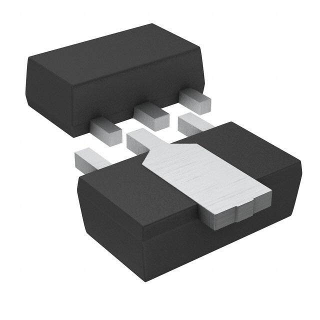
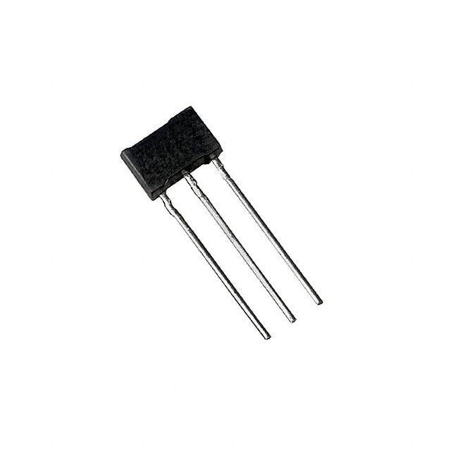
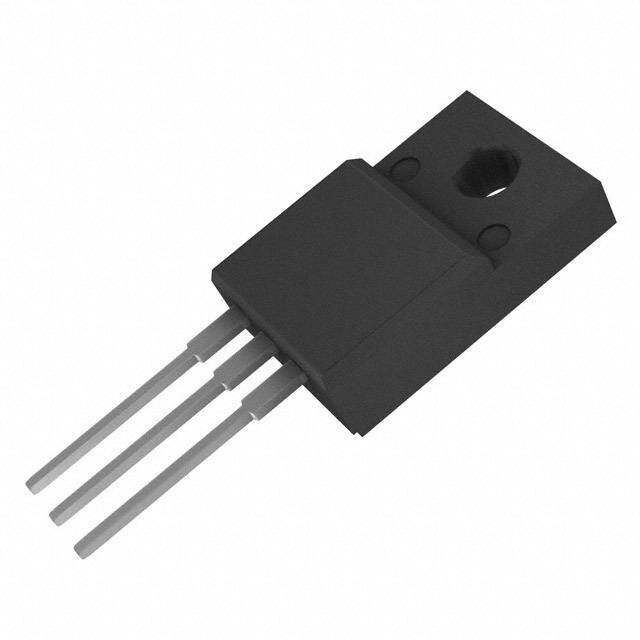

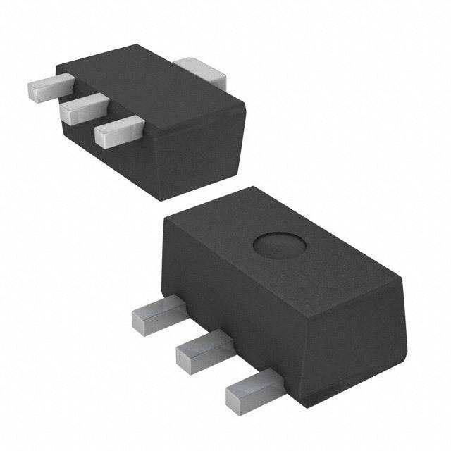
PDF Datasheet 数据手册内容提取
MJ14001 (PNP), MJ14002* (NPN), MJ14003* (PNP) *Preferred Devices High−Current Complementary Silicon Power Transistors Designed for use in high−power amplifier and switching circuit http://onsemi.com applications. Features 60 AMPERE • High Current Capability − I Continuous = 60 Amperes C COMPLEMENTARY SILICON • DC Current Gain − h = 15−100 @ I = 50 Adc FE C POWER TRANSISTORS • Low Collector−Emitter Saturation Voltage −V = 2.5 Vdc (Max) CE(sat) 60−80 VOLTS, 300 WATTS @ I = 50 Adc C • Pb−Free Packages are Available* MAXIMUM RATINGS (TJ = 25°C unless otherwise noted) MARKING DIAGRAM Rating Symbol Value Unit Collector−Emitter Voltage MJ14001 VCEO 60 Vdc MJ14002/03 80 Collector−Base Voltage MJ14001 VCBO 60 Vdc MJ14002/03 80 MJ1400xG Emitter−Base Voltage VEBO 5.0 Vdc AYYWW MEX Collector Current− Continuous IC 60 Adc Base Current − Continuous IB 15 Adc TO−204 (TO−3) Emitter Current − Continuous IE 75 Adc CASE 197A STYLE 1 Total Power Dissipation @ TC = 25°C PD 300 W Derate Above 25°C 1.71 W/°C MJ1400x = Device Code Operating and Storage Junction TJ, Tstg −(cid:2)65 to +200 °C xx = 1, 2, or 3 Temperature Range G = Pb−Free Package Maximum ratings are those values beyond which device damage can occur. A = Location Code Maximum ratings applied to the device are individual stress limit values (not YY = Year normal operating conditions) and are not valid simultaneously. If these limits are WW = Work Week exceeded, device functional operation is not implied, damage may occur and MEX = Country of Orgin reliability may be affected. 360 ORDERING INFORMATION 330 S) Device Package Shipping T T WA 270 MJ14001 TO−3 100 Units/Tray N ( O MJ14001G TO−3 100 Units/Tray ATI 210 (Pb−Free) P SI S MJ14002 TO−3 100 Units/Tray DI 150 ER MJ14002G TO−3 100 Units/Tray W O 90 (Pb−Free) P , D MJ14003 TO−3 100 Units/Tray P 30 MJ14003G TO−3 100 Units/Tray 0 (Pb−Free) 0 40 80 120 160 200 240 T , CASE TEMPERATURE (°C) C Preferred devices are recommended choices for future use Figure 1. Power Derating and best overall value. *For additional information on our Pb−Free strategy and soldering details, please download the ON Semiconductor Soldering and Mounting Techniques Reference Manual, SOLDERRM/D. © Semiconductor Components Industries, LLC, 2005 1 Publication Order Number: December, 2005 − Rev. 6 MJ14001/D
MJ14001 (PNP), MJ14002* (NPN), MJ14003* (PNP) ÎÎÎÎÎÎÎÎÎÎÎÎÎÎÎÎÎÎÎÎÎÎÎÎÎÎÎÎÎÎÎÎÎ THERMAL CHARACTERISTICS ÎÎÎÎÎÎÎÎÎÎÎÎÎÎÎÎÎÎÎÎÎÎÎÎÎÎÎÎÎÎÎÎÎÎÎÎÎÎÎÎÎÎÎÎÎÎÎÎÎÎÎÎÎÎÎÎÎÎÎÎÎÎÎÎÎÎÎÎÎ Characteristic Symbol Max Unit ÎÎÎÎÎÎÎÎÎÎÎÎÎÎÎÎÎÎÎÎÎÎÎÎÎÎÎÎÎÎÎÎÎÎÎÎÎÎÎÎÎÎÎÎÎÎÎÎÎÎÎÎÎÎÎÎÎÎÎÎÎÎÎÎÎÎÎÎÎÎÎÎ Thermal Resistance, Junction−to−Case R(cid:2)JC 0.584 (cid:2)C/W ÎÎÎÎÎÎÎÎÎÎÎÎÎÎÎÎÎÎÎÎÎÎÎÎÎÎÎÎÎÎÎÎÎÎÎÎÎÎÎÎÎÎÎÎÎÎÎÎÎÎÎÎÎÎÎÎÎÎÎÎÎÎÎÎÎÎÎÎÎ ÎÎÎÎELEÎÎCTÎÎRICÎÎAL ÎÎCHAÎÎRAÎÎCTEÎÎRISÎÎTICÎÎS (TÎÎC = ÎÎ25(cid:2)ÎCÎ unÎÎlessÎÎ otheÎÎrwisÎÎe noÎÎted)ÎÎÎÎÎÎÎÎÎÎÎÎÎÎÎÎÎÎÎÎÎÎÎÎÎÎÎÎÎÎÎÎ ÎÎÎÎÎÎÎÎÎÎÎÎÎÎÎÎÎÎÎÎCÎÎharaÎÎcterÎÎisticÎÎÎÎÎÎÎÎÎÎÎÎÎÎÎÎÎÎÎÎÎÎÎSymÎÎbolÎÎÎÎÎMÎÎin ÎÎÎMÎÎaxÎÎÎÎÎUniÎÎt ÎÎÎÎOFFÎÎ CHÎÎARAÎÎCTEÎÎRISÎÎTICSÎÎÎÎÎÎÎÎÎÎÎÎÎÎÎÎÎÎÎÎÎÎÎÎÎÎÎÎÎÎÎÎÎÎÎÎÎÎÎÎÎÎÎÎÎÎÎÎÎÎÎÎÎÎÎÎ ÎÎColÎlectoÎr−EmÎitteÎr SuÎstainÎing VÎoltaÎge (ÎNoteÎ 1) ÎÎÎÎÎÎÎÎÎÎÎÎVÎCEOÎ(sus)ÎÎÎÎÎÎÎÎÎÎVdcÎ (IC = 200 mAdc, IB = 0) MJ14001 60 − ÎÎÎÎÎÎÎÎÎÎÎÎÎÎÎÎÎÎÎÎÎÎÎÎÎÎÎÎÎÎÎÎÎÎÎÎMJ1ÎÎ400ÎÎ2, MÎÎJ140ÎÎ03 ÎÎÎÎÎÎÎÎÎÎÎÎÎÎ8ÎÎ0 ÎÎÎÎÎÎ− ÎÎÎÎÎÎÎÎ ÎÎColÎlectoÎr CuÎtoff CÎurreÎnt ÎÎÎÎÎÎÎÎÎÎÎÎÎÎÎÎÎÎICEÎO ÎÎÎÎÎÎÎÎÎÎmAÎ (VCE = 30 Vdc, IB = 0) MJ14001 − 1.0 ÎÎÎÎÎÎ(VÎÎCE ÎÎ= 40ÎÎ VdcÎÎ, IB =ÎÎ 0) ÎÎÎÎÎÎÎÎÎÎÎÎÎÎÎÎÎÎÎÎMJ1ÎÎ440ÎÎ2, MÎÎJ140ÎÎ03 ÎÎÎÎÎÎÎÎÎÎÎÎÎÎ−ÎÎÎÎÎÎÎÎ1.0 ÎÎÎÎÎÎÎÎ ÎÎColÎlectoÎr CuÎtoff CÎurreÎnt ÎÎÎÎÎÎÎÎÎÎÎÎÎÎÎÎÎÎICEÎX ÎÎÎÎÎÎÎÎÎÎmAÎ ÎÎÎ(VÎCE Î= 60Î VdcÎ, VBÎE(off)Î = 1.Î5 V)Î ÎÎÎÎÎÎÎÎÎMÎJ140Î01 ÎÎÎÎÎÎÎ−ÎÎÎÎ1.0 ÎÎÎÎ (VCE = 80 Vdc, VBE(off) = 1.5 V) MJ14002, MJ14003 − 1.0 ÎÎÎÎÎÎÎÎÎÎÎÎÎÎÎÎÎÎÎÎÎÎÎÎÎÎÎÎÎÎÎÎÎÎÎÎÎÎÎÎÎÎÎÎÎÎÎÎÎÎÎÎÎÎÎÎÎÎÎÎÎÎÎÎÎÎÎÎÎÎÎÎÎÎ Collector Cutoff Current ICBO mA ÎÎÎ(VÎCB Î= 60Î VdcÎ, IE =Î 0) ÎÎÎÎÎÎÎÎÎÎÎÎMÎJ140Î01 ÎÎÎÎÎÎÎ−ÎÎÎÎ1.0 ÎÎÎÎ (VCB = 80 Vdc, IE = 0) MJ14002, MJ14003 − 1.0 ÎÎÎÎÎÎÎÎÎÎÎÎÎÎÎÎÎÎÎÎÎÎÎÎÎÎÎÎÎÎÎÎÎÎÎÎÎÎÎÎÎÎÎÎÎÎÎÎÎÎÎÎÎÎÎÎÎÎÎÎÎÎÎÎÎÎÎÎÎÎÎÎÎÎ Emitter Cutoff Current IEBO − 1.0 mA ÎÎÎÎÎÎ(VÎÎBE ÎÎ= 5.0ÎÎ VdcÎÎ, ICÎ Î= 0)ÎÎÎÎÎÎÎÎÎÎÎÎÎÎÎÎÎÎÎÎÎÎÎÎÎÎÎÎÎÎÎÎÎÎÎÎÎÎÎÎÎÎÎÎÎÎÎÎÎÎÎÎÎÎ ÎÎÎÎON ÎÎCHAÎÎRACÎÎTEÎÎRISTÎÎICSÎÎÎÎÎÎÎÎÎÎÎÎÎÎÎÎÎÎÎÎÎÎÎÎÎÎÎÎÎÎÎÎÎÎÎÎÎÎÎÎÎÎÎÎÎÎÎÎÎÎÎÎÎÎÎÎ ÎÎDC ÎCurrÎent ÎGainÎ (NoÎte 1)ÎÎÎÎÎÎÎÎÎÎÎÎÎÎÎÎÎÎhFÎE ÎÎÎÎÎÎÎÎÎÎ−Î (IC = 25 Adc, VCE = 3.0 V) 30 − ÎÎÎ(IÎC = Î50 AÎdc, VÎCE Î= 3.0Î V)ÎÎÎÎÎÎÎÎÎÎÎÎÎÎÎÎÎÎÎÎ1Î5 ÎÎÎ100ÎÎÎÎ ÎÎÎÎÎÎ(IÎÎC = ÎÎ60 AÎÎdc, VÎÎCE ÎÎ= 3.0ÎÎ V)ÎÎÎÎÎÎÎÎÎÎÎÎÎÎÎÎÎÎÎÎÎÎÎÎÎÎÎÎÎÎÎÎÎÎÎÎÎÎÎÎ5ÎÎ.0 ÎÎÎÎÎÎ− ÎÎÎÎÎÎÎÎ ÎÎColÎlectoÎr−EmÎitteÎr SaÎturatÎion VÎoltaÎge (NÎoteÎ 1) ÎÎÎÎÎÎÎÎÎÎÎÎÎVCEÎ(sat)ÎÎÎÎÎÎÎÎÎÎVdcÎ (IC = 25 Adc, IB = 2.5 Adc) − 1.0 ÎÎÎ(IÎC = Î50 AÎdc, IÎB = 5Î.0 AÎdc)ÎÎÎÎÎÎÎÎÎÎÎÎÎÎÎÎÎÎÎÎ−ÎÎÎÎ2.5 ÎÎÎÎ (IC = 60 Adc, IB = 12 Adc) − 3.0 ÎÎÎÎÎÎÎÎÎÎÎÎÎÎÎÎÎÎÎÎÎÎÎÎÎÎÎÎÎÎÎÎÎÎÎÎÎÎÎÎÎÎÎÎÎÎÎÎÎÎÎÎÎÎÎÎÎÎÎÎÎÎÎÎÎÎÎÎÎÎÎÎÎÎ Base−Emitter Saturation Voltage (Note 1) VBE(sat) Vdc ÎÎÎ(IÎC = Î25 AÎdc, IÎB = 2Î.5 AÎdc)ÎÎÎÎÎÎÎÎÎÎÎÎÎÎÎÎÎÎÎÎ−ÎÎÎÎ2.0 ÎÎÎÎ (IC = 50 Adc, IB = 5.0 Adc) − 3.0 ÎÎÎÎÎÎ(IÎÎC = ÎÎ60 AÎÎdc, IÎÎB = 1ÎÎ2 AÎÎdc) ÎÎÎÎÎÎÎÎÎÎÎÎÎÎÎÎÎÎÎÎÎÎÎÎÎÎÎÎÎÎÎÎÎÎÎÎÎÎ−ÎÎÎÎÎÎÎ4.0 ÎÎÎÎÎÎÎ ÎÎÎÎDYNÎÎAMÎÎIC CÎÎHARÎÎACÎÎTERÎÎISTIÎÎCS ÎÎÎÎÎÎÎÎÎÎÎÎÎÎÎÎÎÎÎÎÎÎÎÎÎÎÎÎÎÎÎÎÎÎÎÎÎÎÎÎÎÎÎÎÎÎÎÎÎÎÎÎ ÎÎOutÎput CÎapaÎcitaÎnceÎÎÎÎÎÎÎÎÎÎÎÎÎÎÎÎÎÎÎCoÎb ÎÎÎ−ÎÎÎ2Î000ÎÎÎpFÎ (VCB = 10 Vdc, IE = 0, f = 0.1 MHz) ÎÎÎÎÎÎÎÎÎÎÎÎÎÎÎÎÎÎÎÎÎÎÎÎÎÎÎÎÎÎÎÎÎÎÎÎÎ 1. Pulse Test: Pulse Width (cid:2) 300 (cid:3)s, Duty Cycle (cid:2) 2.0%. 100 There are two limitations on the power handling ability of 70 5.0 ms 1.0 ms 1.0 (cid:3)s 50 a transistor: average junction temperature and second MP) 2300 dc breakdown. Safe operating area curves indicate IC − VCE A limits of the transistor that must be observed for reliable NT ( 10 operation: i.e., the transistor must not be subjected to greater E 7.0 RR 5.0 TC = 25°C dissipation than the curves indicate. U WIRE BOND LIMIT C 3.0 The data of Figure 2 is based on T = 200(cid:2)C; T is R 2.0 THERMAL LIMIT J(pk) C TO SECOND BREAKDOWN LIMIT variable depending on conditions. Second breakdown pulse C 1.0 LE 0.7 limits are valid for duty cycles to 10% provided TJ(pk) OL 0.5 (cid:2) 200(cid:2)C. T may be calculated from the data in C J(pk) , C0.3 Figure 13. At high case temperatures, thermal limitations I 0.2 MJ14001 MJ14002, MJ14003 will reduce the power that can be handled to values less than 0.1 the limitations imposed by second breakdown. 1.0 2.0 3.0 5.0 7.0 10 20 30 50 70 100 V , COLLECTOR−EMITTER VOLTAGE (VOLTS) CE Figure 2. Maximum Rated Forward Biased Safe Operating Area http://onsemi.com 2
MJ14001 (PNP), MJ14002* (NPN), MJ14003* (PNP) TYPICAL ELECTRICAL CHARACTERISTICS MJ14002 (NPN) MJ14001, MJ14003 (PNP) 300 300 200 200 100 100 N N GAI 70 GAI 70 T 50 T 50 N N E V = 3.0 V E V = 3.0 V R CE R CE UR 30 TJ = −(cid:2)55°C UR 30 TJ = −(cid:2)55°C C C 20 TJ = 25°C C C 20 TJ = 25°C , DE 10 TJ = 150°C , DE 10 TJ = 150°C F F h h 7.0 7.0 5.0 5.0 3.0 3.0 0.7 1.0 2.0 3.0 5.0 7.0 10 20 30 50 70 0.7 1.0 2.0 3.0 5.0 7.0 10 20 30 50 70 IC, COLLECTOR CURRENT (AMPS) IC, COLLECTOR CURRENT (AMPS) Figure 3. DC Current Gain Figure 4. DC Current Gain S) 2.8 S) 2.8 T T L L O O GE (V 2.4 TJ = 25°C IC = 60 A GE (V 2.4 TJ = 25°C IC = 60 A A A T 2.0 T 2.0 L L O O V V R 1.6 R 1.6 E E EMITT 1.2 IC = 25 A EMITT 1.2 IC = 25 A − − R R O O T 0.8 I = 10 A T 0.8 I = 10 A C C C C E E L L L L O 0.4 O 0.4 C C , E , E VC 0 VC 0 0.1 0.2 0.3 0.5 0.7 1.0 2.0 3.0 5.0 7.0 10 0.1 0.2 0.3 0.5 0.7 1.0 2.0 3.0 5.0 7.0 10 IB, BASE CURRENT (AMPS) IB, BASE CURRENT (AMPS) Figure 5. Collector Saturation Region Figure 6. Collector Saturation Region 2.8 2.8 TJ = 25°C TJ = 25°C 2.4 2.4 S) 2.0 S) 2.0 OLT OLT V 1.6 V 1.6 E ( E ( G G V, VOLTA 10..28 VBE(sat) @ IC/IB = 10 V, VOLTA 10..28 VBE(sat) @ IC/IB = 10 V @ V = 3.0 V BE(on) CE V @ V = 3.0 V BE(on) CE 0.4 0.4 V @ I /I = 10 CE(sat) C B V @ I /I = 10 CE(sat) C B 0 0 0.7 1.0 2.0 3.0 5.0 7.0 10 20 30 50 70 0.7 1.0 2.0 3.0 5.0 7.0 10 20 30 50 70 IC, COLLECTOR CURRENT (AMPS) IC, COLLECTOR CURRENT (AMPS) Figure 7. “On” Voltages Figure 8. “On” Voltages http://onsemi.com 3
MJ14001 (PNP), MJ14002* (NPN), MJ14003* (PNP) 1.0 4.0 0.7 3.0 0.5 2.0 t s t r 0.3 1.0 0.2 0.7 (cid:3)(cid:4)s)μ td (cid:3)(cid:4)s)μ 0.5 E ( 0.1 E ( TIM 0.07 TIM 0.3 tf t, 0.05 t, 0.2 0.03 0.1 0.02 MJ14002 (NPN) MJ14002 (NPN) MJ14001, MJ14003 (PNP) 0.07 MJ14001, MJ14003 (PNP) 0.01 0.04 0.7 1.0 2.0 3.0 5.0 7.0 10 20 30 50 70 0.7 1.0 2.0 3.0 5.0 7.0 10 20 30 50 70 I , COLLECTOR CURRENT (AMPS) I , COLLECTOR CURRENT (AMPS) C C Figure 9. Turn−On Switching Times Figure 10. Turn−Off Switching Times V −(cid:2)30 V CC R L +(cid:2)2.0 V R B 0 TO SCOPE 10000 t ≤ 20 ns 7000 tr ≤ −12 V r 20 ns 5000 10 to 100 (cid:3)s DUTY CYCLE ≈ 2.0% F) 3000 VCC −(cid:2)30 V E (p 2000 +10 RL TANC 1000 Cib Cib Cob 0 V RB TO SCOPE PACI 700 Cob tr ≤ 20 ns CA 500 −12 V tr ≤ 20 ns C, TJ = 25°C 10 to 100 (cid:3)s 300 MJ14002 (NPN) DUTY CYCLE ≈ 2.0% VBB 200 MJ14001, MJ14003 (PNP) +(cid:2)7.0 V FOR CURVES OF FIGURES 3 & 6, R & R ARE VARIED. 100 B L 1.0 2.0 3.0 5.0 7.0 10 20 30 50 70 100 INPUT LEVELS ARE APPROXIMATELY AS SHOWN. FOR NPN CIRCUITS, REVERSE ALL POLARITIES. V , REVERSE VOLTAGE (VOLTS) R Figure 11. Capacitance Variation Figure 12. Switching Test Circuit D) E Z LI 1.0 A M 0.7 R D = 0.5 NO 0.5 E ( NC 0.3 0.2 SISTA 0.2 0.1 R(cid:2)JC(t) = r(t) R(cid:2)JC P(pk) RE 0.1 0.05 R(cid:2)JC = 0.584°C/W MAX L D CURVES APPLY FOR POWER RMA 00..0075 0.02 PULSE TRAIN SHOWN t1 HE READ TIME AT t1 t2 NT T 0.03 0.01 TJ(pk) − TC = P(pk) R(cid:2)JC(t) DUTY CYCLE, D = t1/t2 SIE 0.02 SINGLE PULSE N A TR 0.01 r(t), 0.02 0.03 0.05 0.07 0.1 0.2 0.3 0.5 0.7 1.0 2.0 t3, .T0IME5 (.m0s7).0 10 20 30 50 70 100 200 300 5007001000 2000 Figure 13. Thermal Response http://onsemi.com 4
MJ14001 (PNP), MJ14002* (NPN), MJ14003* (PNP) PACKAGE DIMENSIONS TO−204 (TO−3) CASE 197A−05 ISSUE K A NOTES: 1.DIMENSIONING AND TOLERANCING PER N ANSI Y14.5M, 1982. 2.CONTROLLING DIMENSION: INCH. C −T− SEATING INCHES MILLIMETERS PLANE E DIM MIN MAX MIN MAX A 1.530 REF 38.86 REF D 2 PL K B 0.990 1.050 25.15 26.67 0.30 (0.012)M T Q M Y M C 0.250 0.335 6.35 8.51 D 0.057 0.063 1.45 1.60 E 0.060 0.070 1.53 1.77 G 0.430 BSC 10.92 BSC H 0.215 BSC 5.46 BSC K 0.440 0.480 11.18 12.19 U −Y− L 0.665 BSC 16.89 BSC V L N 0.760 0.830 19.31 21.08 Q 0.151 0.165 3.84 4.19 2 U 1.187 BSC 30.15 BSC G B V 0.131 0.188 3.33 4.77 H 1 STYLE 1: PIN 1.BASE 2.EMITTER −Q− CASE:COLLECTOR 0.25 (0.010)M T Y M ON Semiconductor and are registered trademarks of Semiconductor Components Industries, LLC (SCILLC). SCILLC reserves the right to make changes without further notice to any products herein. SCILLC makes no warranty, representation or guarantee regarding the suitability of its products for any particular purpose, nor does SCILLC assume any liability arising out of the application or use of any product or circuit, and specifically disclaims any and all liability, including without limitation special, consequential or incidental damages. “Typical” parameters which may be provided in SCILLC data sheets and/or specifications can and do vary in different applications and actual performance may vary over time. All operating parameters, including “Typicals” must be validated for each customer application by customer’s technical experts. SCILLC does not convey any license under its patent rights nor the rights of others. SCILLC products are not designed, intended, or authorized for use as components in systems intended for surgical implant into the body, or other applications intended to support or sustain life, or for any other application in which the failure of the SCILLC product could create a situation where personal injury or death may occur. Should Buyer purchase or use SCILLC products for any such unintended or unauthorized application, Buyer shall indemnify and hold SCILLC and its officers, employees, subsidiaries, affiliates, and distributors harmless against all claims, costs, damages, and expenses, and reasonable attorney fees arising out of, directly or indirectly, any claim of personal injury or death associated with such unintended or unauthorized use, even if such claim alleges that SCILLC was negligent regarding the design or manufacture of the part. SCILLC is an Equal Opportunity/Affirmative Action Employer. This literature is subject to all applicable copyright laws and is not for resale in any manner. PUBLICATION ORDERING INFORMATION LITERATURE FULFILLMENT: N. American Technical Support: 800−282−9855 Toll Free ON Semiconductor Website: http://onsemi.com Literature Distribution Center for ON Semiconductor USA/Canada P.O. Box 61312, Phoenix, Arizona 85082−1312 USA Order Literature: http://www.onsemi.com/litorder Phone: 480−829−7710 or 800−344−3860 Toll Free USA/Canada Japan: ON Semiconductor, Japan Customer Focus Center Fax: 480−829−7709 or 800−344−3867 Toll Free USA/Canada 2−9−1 Kamimeguro, Meguro−ku, Tokyo, Japan 153−0051 For additional information, please contact your Email: orderlit@onsemi.com Phone: 81−3−5773−3850 local Sales Representative. http://onsemi.com MJ14001/D 5
Mouser Electronics Authorized Distributor Click to View Pricing, Inventory, Delivery & Lifecycle Information: O N Semiconductor: MJ14002G
 Datasheet下载


