ICGOO在线商城 > 射频/IF 和 RFID > RF 接收器 > MICRF220AYQS

 Datasheet下载
- 型号: MICRF220AYQS
- 制造商: Micrel
- 库位|库存: xxxx|xxxx
- 要求:
| 数量阶梯 | 香港交货 | 国内含税 |
| +xxxx | $xxxx | ¥xxxx |
查看当月历史价格
查看今年历史价格
MICRF220AYQS产品简介:
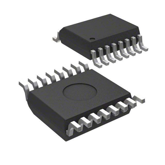
ICGOO电子元器件商城为您提供MICRF220AYQS由Micrel设计生产,在icgoo商城现货销售,并且可以通过原厂、代理商等渠道进行代购。 MICRF220AYQS价格参考。MicrelMICRF220AYQS封装/规格:RF 接收器, QwikRadio® RF Receiver ASK, OOK 300MHz ~ 450MHz -112.5dBm 20kbps PCB, Surface Mount 16-QSOP。您可以下载MICRF220AYQS参考资料、Datasheet数据手册功能说明书,资料中有MICRF220AYQS 详细功能的应用电路图电压和使用方法及教程。
| 参数 | 数值 |
| 产品目录 | |
| 描述 | RCVR ASK/OOK 300-450MHZ 16QSOP射频接收器 300MHz to 450MHz, 3.0V to 3.6V, 6mA, <10kbps ASK Receiver with RSSI and Shutdown |
| 产品分类 | |
| 品牌 | Micrel |
| 产品手册 | |
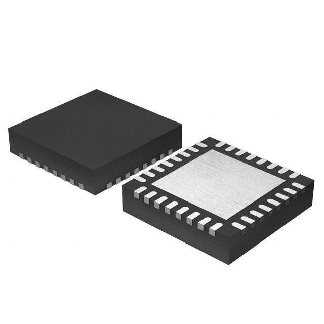
| 产品图片 |
|
| rohs | 符合RoHS无铅 / 符合限制有害物质指令(RoHS)规范要求 |
| 产品系列 | RF集成电路,射频接收器,Micrel MICRF220AYQSQwikRadio® |
| 数据手册 | |
| 产品型号 | MICRF220AYQS |
| 产品种类 | 射频接收器 |
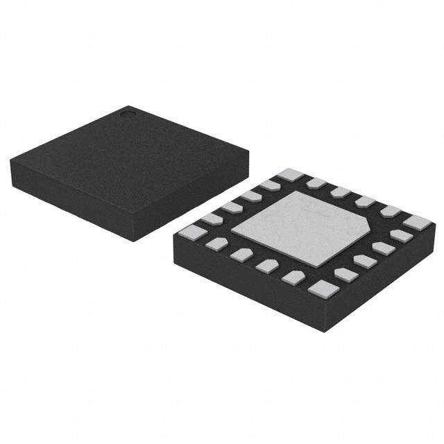
| 供应商器件封装 | 16-QSOP |
| 其它名称 | 576-3742-5 |
| 包装 | 管件 |
| 商标 | Micrel |
| 天线连接器 | PCB,表面贴装 |
| 存储容量 | - |
| 安装风格 | SMD/SMT |
| 封装 | Tube |
| 封装/外壳 | 16-SSOP(0.154",3.90mm 宽) |
| 封装/箱体 | QSOP-16 |
| 工作温度 | -40°C ~ 105°C |
| 工作电源电压 | 3 V to 3.6 V |
| 工作频率 | 300 MHz to 450 MHz |
| 工厂包装数量 | 98 |
| 带宽 | 330 kHz |
| 应用 | 通用 |
| 数据接口 | PCB,表面贴装 |
| 数据速率(最大值) | 20kbps |
| 最大工作温度 | + 105 C |
| 最小工作温度 | - 40 C |
| 标准包装 | 98 |
| 灵敏度 | -112.5dBm |
| 特性 | 配有 RSSI |
| 电压-电源 | 3 V ~ 3.6 V |
| 电流-接收 | 6mA |
| 电源电压-最大 | 3.6 V |
| 电源电压-最小 | 3 V |
| 电源电流 | 4.3 mA |
| 类型 | RF Receiver |
| 系列 | MICRF220 |
| 调制或协议 | ASK,OOK |
| 配用 | /product-detail/zh/ABM7-9.81563MHZ-10-R50-J4Q-T/535-10154-6-ND/2184281/product-detail/zh/ABLS-13.52127MHZ-10-J-4Q-T/535-10148-6-ND/2184275/product-detail/zh/ABM7-9.81563MHZ-10-R50-J4Q-T/535-10154-1-ND/2184189/product-detail/zh/ABM7-13.52127MHZ-10-R50-J4Q-T/535-10153-1-ND/2184188/product-detail/zh/ABLS-13.52127MHZ-10-J-4Q-T/535-10148-1-ND/2184183/product-detail/zh/ABM7-9.81563MHZ-10-R50-J4Q-T/535-10154-2-ND/2184097/product-detail/zh/ABM7-13.52127MHZ-10-R50-J4Q-T/535-10153-2-ND/2184096/product-detail/zh/ABLS-13.52127MHZ-10-J-4Q-T/535-10148-2-ND/2184091 |
| 频率 | 300MHz ~ 450MHz |


_renders/CS4265-CNZR.jpg)

- 商务部:美国ITC正式对集成电路等产品启动337调查
- 曝三星4nm工艺存在良率问题 高通将骁龙8 Gen1或转产台积电
- 太阳诱电将投资9.5亿元在常州建新厂生产MLCC 预计2023年完工
- 英特尔发布欧洲新工厂建设计划 深化IDM 2.0 战略
- 台积电先进制程称霸业界 有大客户加持明年业绩稳了
- 达到5530亿美元!SIA预计今年全球半导体销售额将创下新高
- 英特尔拟将自动驾驶子公司Mobileye上市 估值或超500亿美元
- 三星加码芯片和SET,合并消费电子和移动部门,撤换高东真等 CEO
- 三星电子宣布重大人事变动 还合并消费电子和移动部门
- 海关总署:前11个月进口集成电路产品价值2.52万亿元 增长14.8%


PDF Datasheet 数据手册内容提取
MICRF220 300MHz to 450MHz, 3.3V ASK/OOK Receiver with RSSI and Squelch General Description Features The MICRF220 is a 300MHz to 450MHz super- • –110dBm sensitivity at 1kbps with 0.1% BER heterodyne, image-reject, RF receiver with automatic • Supports bit rates up to 20kbps at 433.92MHz gain control, ASK/OOK demodulator, analog RSSI • 25dB image-reject mixer output, and integrated squelch features. It only requires a crystal and a minimum number of external components • No IF filter required to implement. The MICRF220 is ideal for low-cost, low- • 60dB analog RSSI output range power, RKE, TPMS, and remote actuation applications. • 3.0V to 3.6V supply voltage range The MICRF220 achieves −110dBm sensitivity at a bit • 4.3mA supply current at 315MHz rate of 1kbps with 0.1% BER. Four demodulator filter • 6.0mA supply current at 434MHz bandwidths are selectable in binary steps from 1625Hz • 0.1µA supply current in shutdown mode to 13kHz at 433.92MHz, allowing the device to support bit rates up to 20kbps. The device operates from a • Data output squelch until valid bits detected supply voltage of 3.0V to 3.6V, and typically consumes • 16-pin QSOP package (4.9mm x 6.0mm) 4.3mA of supply current at 315MHz and 6.0mA at • −40˚C to +105˚C temperature range 433.92MHz. A shutdown mode reduces supply current to • 3kV HBM ESD Rating 0.1μA typical. The squelch feature decreases the activity on the data output pin until valid bits are detected while maintaining overall receiver sensitivity. Datasheets and support documentation can be found on Micrel’s website at: www.micrel.com. Typical Application 433.92MHz, 1kbps Operation Micrel Inc. • 2180 Fortune Drive • San Jose, CA 95131 • USA • tel +1 (408) 944-0800 • fax + 1 (408) 474-1000 • http://www.micrel.com August 19, 2015 Revision 2.0 RadioTech@micrel.com or (408) 944-0800
Micrel, Inc. MICRF220 Ordering Information Part Number Temperature Range Package MICRF220AYQS –40°C to +105°C 16-Pin QSOP Pin Configuration MICRF220AYQS Pin Description Pin Pin Pin Function Number Name Reference resonator connection to the Pierce oscillator. May also be driven by external reference signal of 1 RO1 200mVp-p to 1.5V p-p amplitude maximum. Internal capacitance of 7pF to GND during normal operation. 2 GNDRF Ground connection for ANT RF input. Connect to PCB ground plane. Antenna Input: RF Signal Input from Antenna. Internally AC coupled. It is recommended to use a matching 3 ANT network with an inductor-to-RF ground to improve ESD protection. 4 GNDRF Ground connection for ANT RF input. Connect to PCB ground plane. Positive supply connection for all chip functions. Bypass with 0.1μF capacitor located as close to the VDD pin 5 VDD as possible. Squelch Control Logic-Level Input. An internal pull-up (5μA typical) pulls the logic-input HIGH when the device 6 SQ is enabled. A logic LOW on SQ squelches, or reduces, the random activity on DO pin when there is no RF input signal. Demodulator Filter Bandwidth Select Logic-Level Input. This pin has an internal pull-up (3μA typical) when the 7 SEL0 chip is on. Use in conjunction with SEL1 to control demodulation bandwidth. Shutdown Control Logic-Level Input. A logic-level LOW enables the device. A logic-level HIGH places the 8 SHDN device in low-power shutdown mode. An internal pull-up (5μA typical) pulls the logic input HIGH. 9 GND Ground connection for all chip functions except for RF input. Connect to PCB ground plane. Data Output. Demodulated data output. A current limited CMOS output during normal operation, 25kΩ pull- 10 DO down is present when device is in shutdown. Demodulator Filter Bandwidth Select Logic-Level Input. This pin has an internal pull-up (3μA typical) when the 11 SEL1 chip is on. Use in conjunction with SEL0 to Demodulation bandwidth. Demodulation Threshold Voltage Integration Capacitor. Connect a 0.1μF capacitor from CTH pin-to-GND to 12 CTH provide a stable slicing threshold. AGC Filter Capacitor. Connect a capacitor from this pin to GND. Refer to the AGC Loop and CAGC section for 13 CAGC information on the capacitor value. Received Signal Strength Indicator. The voltage on this pin is an inversed amplified version of the voltage on 14 RSSI CAGC. Output is from a switched capacitor integrating op amp with 250Ω typical output impedance. 15 NC No Connect. Leave this pin floating. Reference resonator connection to the Pierce oscillator. Internal capacitance of 7pF to GND during normal 16 RO2 operation. August 19, 2015 2 Revision 2.0
Micrel, Inc. MICRF220 (1) (2) Absolute Maximum Ratings Operating Ratings Supply Voltage (V ) .................................................. +5V Supply Voltage (V ) ............................. +3.0V to +3.6V DD DD ANT, SQ, SEL0, SEL1, Ambient Temperature (T ).................. –40°C to +105°C A SHDN DC Voltage. .................... −0.3V to V + 0.3V ANT, SQ, SEL0, SEL1, DD Junction Temperature ........................................... +150ºC SHDN DC Voltage ................ ....−0.3V to V + 0.3V DD Lead Temperature (soldering, 10sec.) .................. +300°C Maximum Input RF Power .................................. 0 dBm Storage Temperature ............................. −65ºC to +150°C Receive Modulation Duty Cycle ....................... 20~80% Maximum Receiver Input Power ......................... +10dBm Frequency Range .......................... 300MHz to 450MHz ESD Rating(3) .................................................... 3kV HBM Electrical Characteristics VDD = 3.3V, VSHDN = GND = 0V, SQ = open, CCAGC = 4.7µF, CCTH = 0.1µF, unless otherwise noted. Bold values indicate –40°C ≤ TA ≤ 105°C. “Bit rate” refers to the encoded bit rate throughout this datasheet (see Note 4). Parameter Condition Min. Typ. Max. Units Continuous Operation, fRF = 315MHz 4.3 Operating Supply Current mA Continuous Operation, fRF = 433.92MHz 6.0 Shutdown Current VSHDN = VDD 0.1 µA Receiver 433.92MHz, VSEL1 = VSEL0 = 0V, BER = 1% −112.5 433.92MHz, VSEL1 = VSEL0 = 0V, −110 BER = 0.1% Conducted Receiver dBm Sensitivity@1kbps (Note 5) 315MHz, VSEL1 = 0V, VSEL0 = 3.3V, −112.5 BER = 1% 315MHz, VSEL1 = 0V, VSEL0 = 3.3V, −110 BER = 0.1% Image Rejection fIMAGE = fRF – 2fIF 25 dB fRF = 315MHz 0.85 IF Center Frequency (fIF) MHz fRF = 433.92MHz 1.18 fRF = 315MHz 235 −3dB IF Bandwidth kHz fRF = 433.92MHz 330 −40dBm RF input level 1.15 CAGC Voltage Range V −100dBm RF input level 1.55 Reference Oscillator Reference Oscillator fRF = 315 MHz 9.81713 MHz Frequency fRF = 433.92 MHz 13.52313 Reference Buffer Input RO1 when driven externally 1.6 kΩ Impedance Reference Oscillator Bias RO2 1.15 V Voltage Reference Oscillator Input Range External input, AC couple to RO1 0.2 1.5 VP-P Reference Oscillator Source Current VRO1 = 0V 300 µA August 19, 2015 3 Revision 2.0
Micrel, Inc. MICRF220 Electrical Characteristics (Continued) Parameter Condition Min. Typ. Max. Units Demodulator CTH Source Impedance, fREF = 9.81713MHz 165 kΩ Note 6 fREF = 13.52313MHz 120 CTH Leakage Current In TA = +25ºC 1 nA CTH Hold Mode TA = +105ºC 10 Digital / Control Functions DO Pin Output Current As output source @ 0.8 VDD 300 µA As output sink @ 0.2 VDD 680 Output Rise Time 15pF load on DO pin, transition time 600 ns Output Fall Time between 0.1xVDD and 0.9xVDD 200 Input High Voltage SHDN, SEL0, SEL1, SQ 0.8VDD V Input Low Voltage SHDN, SEL0, SEL1, SQ 0.2VDD V Output Voltage High DO 0.8VDD V Output Voltage Low DO 0.2VDD V RSSI RSSI DC Output Voltage −110dBm RF input level 0.5 V Range −50dBm RF input level 2.0 RSSI Output Current 5kΩ load to GND, −50dBm RF input level 400 µA RSSI Output Impedance 250 Ω RSSI Response Time VSEL0 = VSEL1 = 0V, RF input power stepped 10 ms from no input to −50dBm Notes: 1. Exceeding the absolute maximum rating may damage the device. 2. The device is not guaranteed to function outside of its operating rating. 3. Device is ESD sensitive. Use appropriate ESD precautions. Exceeding the absolute maximum rating may damage the device. 4. Encoded bit rate is 1/(shortest pulse duration) that appears at MICRF220 DO pin. 5. In an ON/OFF keyed (OOK) signal, the signal level goes between a “mark” level (when the RF signal is ON) and a “space” level (when the RF signal is OFF). Sensitivity is defined as the input signal level when “ON” necessary to achieve a specified BER (bit error rate). BER measured with the built-in BERT function in Agilent E4432B using the PN9 sequence. Sensitivity measurement values are obtained using an input matching network corresponding to 315MHz or 433.92MHz. 6. CTH source impedance is inversely proportional to the reference frequency. In production testing, the typical source impedance value is verified with 12MHz reference frequency. August 19, 2015 4 Revision 2.0
Micrel, Inc. MICRF220 Typical Characteristics VDD = 3.3V, TA = +25ºC, BER measured with PN9 sequence, unless otherwise noted. Current vs. Receiver Current vs. Supply Voltage Current vs. Supply Voltage Frequency fRF = 433.92MHz fRF = 315MHz 6.5 7.5 5.0 +105ºC +105ºC 6.0 7.0 mA)5.5 mA) 6.5 mA)4.5 Current (45..50 Current ( 56..50 +25ºC Current (4.0 +25ºC 4.0 5.0 -40ºC -40ºC 3.5 4.5 3.5 300 325 350 375 400 425 450 3.0 3.2 3.4 3.6 3.0 3.2 3.4 3.6 Receiver Frequency (MHz) Supply Voltage (V) Supply Voltage (V) CAGC Voltage vs. Input BER vs. Input Power RSSI vs. Input Power Power V = V = 0V SEL1 SEL0 2.5 10 2.0 2.0 C Voltage (V) 111...468 +105ºC-40ºC SSI Voltage (V)11..05 +25ºC +105ºC -40ºC BER (%) 1 315MHz ` 433.92MHz G +25ºC R A C1.2 0.5 PN9 sequence at 1kbps 1.0 0.0 0.1 -125 -100 -75 -50 -25 0 -125 -100 -75 -50 -25 0 -116 -115 -114 -113 -112 -111 -110 Input Power (dBm) Input Power (dBm) Input Power (dBm) Sensitivity at 1% BER Sensitivity at 1% BER Sensitivity at 1% BER VSEL1 = VSEL0 = 0V VSEL1 = 0V, VSEL0 = 3.3V VSEL1 = 3.3V, VSEL0 = 0V -98 -100 -98 -100 -102 -100 -102 m) m) -104 m) -102 B-104 B B d d d Sensitivity (---111100086 315MHz 433.92MHz Sensitivity ( ---111100086 315MHz 433.92MHz Sensitivity ( ---111000864 315MHz 433.92MHz -112 -114 -112 -110 -116 -114 -112 0 2 4 6 8 10 12 0 3 6 9 12 15 18 21 0 10 20 30 40 Bit Rate (kbps) Bit Rate (kbps) Bit Rate (kbps) August 19, 2015 5 Revision 2.0
Micrel, Inc. MICRF220 Typical Characteristics (Continued) VDD = 3.3V, TA = +25ºC, BER measured with PN9 sequence, unless otherwise noted. Sensitivity at 1% BER Bandpass Filter Attenuation Bandpass Filter Attenuation VSEL1 = 3.3V, VSEL0 = 3.3V fXTAL = 13.52313MHz fXTAL = 9.81713MHz -98 1 1 0 0 -100 -1 -1 m) B) -2 B) -2 dB -102 n (d --43 n (d --43 Sensitivity ( --110064 315MHz Attenuatio ----8765 Attenuatio ----8765 433.92MHz -9 -9 -108 -10 -10 -11 -11 -110 433.6 433.8 434.0 434.2 314.8 314.9 315.0 315.1 315.2 0 10 20 30 40 50 Bit Rate (kbps) Input Frequency (MHz) Input Frequency (MHz) Sensitivity for 1% BER vs Sensitivity for 1% BER vs Frequency Frequency f = 13.52313MHz f = 9.81713MHz XTAL XTAL -40 -40 -50 -50 m) -60 m) -60 B B d -70 d -70 y ( y ( vit -80 vit -80 siti -90 siti -90 n n e e S -100 S -100 -110 -110 -120 -120 419 424 429 434 439 444 449 304 309 314 319 324 Input Frequency (MHz) Input Frequency (MHz) August 19, 2015 6 Revision 2.0
Micrel, Inc. MICRF220 Functional Diagram Figure 1. Simplified Block Diagram August 19, 2015 7 Revision 2.0
Micrel, Inc. MICRF220 Functional Description Therefore, the reference frequency fREF needed for a given desired RF frequency (f ) is approximately: RF The simplified block diagram (Figure 1) illustrates the basic structure of the MICRF220 receiver. It is made up of four sub-blocks: 87 f = f / (32 + ) Eq. 3 REF RF • UHF Down-Converter 1000 • ASK/OOK Demodulator • Reference and Control logic • Squelch Control Outside the device, the MICRF220 receiver requires just a few components to operate: a capacitor from CAGC to GND, a capacitor from CTH-to-GND, a reference crystal resonator with associated loading capacitors, LNA input matching components, and a power-supply decoupling capacitor. Receiver Operation Figure 2. Low-Side Injection Local Oscillator UHF Downconverter The UHF down-converter has six sub-blocks: LNA, mixers, synthesizer, image reject filter, band pass filter and IF Image-Reject Filter and Band-Pass Filter amplifier. The IF ports of the mixer produce quadrature-down converted IF signals. These IF signals are low-pass filtered LNA to remove higher-frequency products prior to the image The RF input signal is AC-coupled into the gate of the LNA reject filter where they are combined to reject the image input device. The LNA configuration is a cascoded frequency. The IF signal then passes through a third order common source NMOS amplifier. The amplified RF signal band pass filter. The IF bandwidth is 330kHz @ is then fed to the RF ports of two double balanced mixers. 433.92MHz, and will scale with RF operating frequency according to: Mixers and Synthesizer The LO ports of the mixers are driven by quadrature local oscillator outputs from the synthesizer block. The local Operating Freq (MHz) BW = BW × Eq. 4 oscillator signal from the synthesizer is placed on the low IF IF@433.92 MHz 433.92 side of the desired RF signal (Figure 2). The product of the incoming RF signal and local oscillator signal will yield the IF frequency, which will be demodulated by the detector of These filters are fully integrated inside the MICRF220. the device. The image reject mixer suppresses the image After filtering, four active gain controlled amplifier stages frequency which is below the wanted signal by two times enhance the IF signal to its proper level for demodulation. the IF frequency. The local oscillator frequency (f ) is set LO to 32 times the crystal reference frequency (fREF) via a ASK/OOK Demodulator phase-locked loop synthesizer with a fully-integrated loop The demodulator section is comprised of detector, filter: programmable low pass filter, slicer, and AGC comparator. f = 32 x f Eq. 1 LO REF MICRF220 uses an IF frequency scheme that scales the IF frequency (f ) with f according to: IF REF 87 f = f x Eq. 2 IF REF 1000 August 19, 2015 8 Revision 2.0
Micrel, Inc. MICRF220 Detector and Programmable Low-Pass Filter Slicer and CTH The demodulation starts with the detector removing the The signal prior to the slicer, labeled “Audio Signal” in carrier from the IF signal. Post detection, the signal Figure 1, is still baseband analog signal. The data slicer becomes baseband information. The low-pass filter further converts the analog signal into ones and zeros based upon enhances the baseband signal. There are four selectable 50% of the slicing threshold voltage built up in the CTH low-pass filter BW settings; 1625Hz, 3250Hz, 6500Hz, and capacitor. After the slicer, the signal is demodulated OOK 13000Hz for 433.92MHz operation. The low-pass filter BW digital data. When there is only thermal noise at ANT pin, is directly proportional to the crystal reference frequency, the voltage level on CTH pin is about 650mV. This voltage and hence RF Operating Frequency. Filter BW values can starts to drop when there is RF signal present. When the be easily calculated by direct scaling. Equation 5 illustrates RF signal level is greater than −100dBm, the voltage is filter Demod BW calculation: about 400mV. The value of the capacitor from CTH pin to GND is not BW = BW × critical to the sensitivity of MICRF220, although it should be Operating Freq @433.92MHz large enough to provide a stable slicing level for the Operating Freq (MHz) Eq. 5 comparator. The value used in the evaluation board of 433.92 0.1μF is good for all bit rates from 500bps to 20kbps. CTH Hold Mode It is very important to choose the baseband bandwidth If the internal demodulated signal (DO′ in Figure 1) is at setting suitable for the data rate to minimize bit error rate. logic LOW for more than about 4msec, the chip Use the operating curves that show BER vs. bit rates for automatically enters CTH hold mode, which holds the different SEL1, SEL0 settings as a guide. voltage on CTH pin constant even without RF input signal. This low-pass filter -3dB corner, or the demodulation BW, This is useful in a transmission gap, or “deadtime”, used in is set at 13000Hz @ 433.92MHz as default (assuming both many encoding schemes. When the signal reappears, CTH SEL0 and SEL1 pins are floating, internal pull-up resistors voltage does not need to re-settle, improving the time to set the voltage to VDD). The low-pass filter can be hardware output with no pulse width distortion, or time to good data set by external pins SEL0 and SEL1. Table 2 demonstrates (TTGD). the scaling for 315MHz RF frequency: AGC Loop and CAGC The AGC comparator monitors the signal amplitude from Low-Pass Maximum Encoded VSEL1 VSEL0 the output of the programmable low-pass filter. The AGC Filter BW Bit Rate loop in the chip regulates the signal at this point to be at a GND GND 1625Hz 2.5kbps constant level when the input RF signal is within the AGC GND VDD 3250Hz 5kbps loop dynamic range (about −115dBm to −40dBm). VDD GND 6500Hz 10kbps When the chip first turns on, the fast charge feature VDD VDD 13000Hz 20kbps charges the CAGC node up with 120µA typical current. When the voltage on CAGC increases, the gains of the Table 1. Low-Pass Filter Selection @ 434MHz RF Input mixer and IF amplifier go up, increasing the amplitude of the audio signal (as labeled in Figure 1), even with only thermal noise at the LNA input. The fast-charge current is disabled when the audio signal crosses the slicing Low-Pass Maximum Encoded VSEL1 VSEL0 threshold, causing DO’ to go high, for the first time. Filter BW Bit Rate When an RF signal is applied, a fast attack period ensues, GND GND 1170Hz 1.8kbps when 600µA current discharges the CAGC node to reduce GND VDD 2350Hz 3.6kbps the gain to a proper level. Once the loop reaches VDD GND 4700Hz 7.2kbps equilibrium, the fast attack current is disabled, leaving only 15µA to discharge CAGC or 1.5µA to charge CAGC. The VDD VDD 9400Hz 14.4kbps fast attack current is enabled only when the RF signal increases faster than the ability of the AGC loop to track it. Table 2. Low-Pass Filter Selection @ 315MHz RF Input August 19, 2015 9 Revision 2.0
Micrel, Inc. MICRF220 The value of CAGC impacts the time to good data (TTGD), which is defined as the time when signal is first applied, to when the pulse width at DO is within 10% of the steady state value. The optimal value of CAGC depends upon the setting of the SEL0 and SEL1 pins. A smaller CAGC value does NOT always result in a shorter TTGD. This is due to the loop dynamics, the fast discharge current being 600µA, and the charge current being only 1.5µA. For example, if V = V = 0V, the low pass filter bandwidth is set to a SEL0 SEL1 minimum and CAGC capacitance is too small, TTGD will be longer than if CAGC capacitance is properly chosen. This is because when RF signal first appears, the fast discharge period will reduce V very fast, lowering the CAGC gain of the mixer and IF amplifier. But since the low pass filter bandwidth is low, it takes too long for the AGC comparator to see a reduced level of the audio signal, so it can not stop the discharge current. This causes an undershoot in CAGC voltage and a corresponding Figure 3. RSSI Overshoot and Slow TTGD (9.1ms) overshoot in RSSI voltage. Once CAGC undershoots, it takes a long time for it to charge back up because the Figure 4 shows the behavior with a larger capacitor on current available is only 1.5µA. CAGC pin (2.2μF), V = 0V, and V = V . In this SEL1 SEL0 DD Table 3 lists the recommended CAGC values for different case, V does not undershoot (RSSI does not CAGC SEL0 and SEL1 settings. overshoot), and TTGD is relatively short at 1ms. VSEL1 VSEL0 CAGC value 0V 0V 4.7μF 0V VDD 2.2μF VDD 0V 1μF VDD VDD 0.47μF Table 3. Minimum Suggested CAGC Values Figure 3 illustrates what occurs if CAGC capacitance is too small for a given SEL1, SEL0 setting. Here, V = 0V, SEL1 V = V , the capacitance on CAGC pin is 0.47μF, and SEL0 DD the RF input level is stepped from no signal to −100dBm. RSSI voltage is shown instead of CAGC voltage because RSSI is a buffered version of CAGC (with an inversion and amplification). Probing CAGC directly can affect the loop dynamics through resistive loading from a scope probe, especially in the state where only 1.5μA is available, Figure 4. Proper TTGD (1ms) with Sufficient CAGC whereas probing RSSI does not. When RF signal is first applied, RSSI voltage overshoots due to the fast discharge current on CAGC, and the loop is too slow to stop this fast Reference Oscillator discharge current in time. Since the voltage on CAGC is The reference oscillator in the MICRF220 (Figure 5) uses a too low, the audio signal level is lower than the slicing basic Pierce crystal oscillator configuration with MOS threshold (voltage on CTH), and DO pin is low. Once the transconductor to provide negative resistance. Though the fast discharge current stops, only the small 1.5µA charge MICRF220 has built-in load capacitors for the crystal current is available in settling the AGC loop to the correct oscillator, the external load capacitors are still required for level, causing the recovery from CAGC undershoot/RSSI tuning it to the right frequency. RO1 and RO2 are external overshoot condition to be slow. As a result, TTGD is about pins of the MICRF220 to connect the crystal to the 9.1ms. reference oscillator. August 19, 2015 10 Revision 2.0
Micrel, Inc. MICRF220 RO2 C V BIAS R RO1 C Figure 5. Reference Oscillator Circuit Reference oscillator crystal frequency can be calculated according to Equation 3. For example, if f = 433.92MHz, RF f = 13.52313MHz. Table 4 lists the values of reference REF frequencies at different popular RF frequencies. To operate the MICRF220 with minimum offset, use proper loading capacitance recommended by the crystal manufacturer. Figure 6. Data Out Pin with No Squelch (VSQ = VDD) When squelch function is enabled by tying the SQ pin low, RF Input Frequency (MHz) Reference Frequency (MHz) the chip will monitor incoming pulse width before allowing 315.0 9.81713* activity on DO pin. The pulse width is set by SEL1 and 390.0 12.15446 SEL0 pins as shown in Table 5, and is inversely proportional to frequency. When there is no input signal 418.0 13.02708 and squelch is not enabled (SQ pin left floating), voltage on 433.92 13.52313* DO chatters due to random noise as shown in Figure 6. If *Empirically derived, slightly different from Equation 3. SQ pin is tied low, the activity on DO pin is much reduced as shown in Figure 7. Table 4. Reference Frequency Examples Squelch Operation When squelch function is enabled by tying the SQ pin low, the chip will monitor incoming pulse width before allowing activity on DO pin. The pulse width is set by SEL1 and SEL0 pins as shown in Table 5, and is inversely proportional to frequency. When there is no input signal and squelch is not enabled (SQ pin left floating), voltage on DO chatters due to random noise as shown in Figure 6. If SQ pin is tied low, the activity on DO pin is much reduced as shown in Figure 7. Figure 7. Data Out Pin with Squelch (VSQ = 0V) August 19, 2015 11 Revision 2.0
Micrel, Inc. MICRF220 When four or less out of eight pulses (at DO′signal labeled Pulse Width at Pulse Width at in Figure 1) are good, the DO output is squelched. If good VSEL1 VSEL0 315MHz (μs) 433.92MHz pulse count increases to seven or more in any eight (μs) sequential pulses, squelch is disabled, thereby allowing 0V 0V 420 305 data to output at DO pin. A good pulse has a duration that is greater than the values listed in Table 5, and it can be a 0V VDD 210 152 high or a low pulse. For other frequencies pulse times are VDD 0V 105 76 calculated as follows: VDD VDD 53 38 Table 5. Pulse Width Settings in Squelch PW = PW@433.92 MHz × 433.92 Eq. 6 Operating Freq(MHz) August 19, 2015 12 Revision 2.0
Micrel, Inc. MICRF220 Application Information Figure 8. MICRF220 EV Board Application Example August 19, 2015 13 Revision 2.0
Micrel, Inc. MICRF220 always inside the IF bandwidth of MICRF220. From this Supply Voltage Ramping consideration, the tolerance should be ±50ppm on both When supply voltage is initially applied, it should rise the transmitter and the MICRF220 side. ESR should be monotonically from 0V to 3.3V to ensure proper startup less than 300Ω, and the temperature range of the crystal of the crystal oscillator and the PLL. It should not have should match the range required by the application. multiple bounces across 2.6V, which is the threshold of With the Abracon crystal listed in the Bill of Materials, a the undervoltage lockout (UVLO) circuit inside typical MICRF220 crystal oscillator still starts up at MICRF220. 105ºC with additional 400Ω series resistance. The oscillator of the MICRF220 is a Pierce-type Antenna and RF Port Connections oscillator. Good care must be taken when laying out the Figure 8 shows the schematic of the MICRF220 printed circuit board. Avoid long traces and place the Evaluation Board. Figures 9 thru 11 depict PCB images. ground plane on the top layer close to the REFOSC pins This evaluation board is a good starting point for the RO1 and RO2. When care is not taken in the layout, and prototyping of most applications. The evaluation board the crystals used are not verified, the oscillator may not offers two options of injecting the RF input signal: start or takes longer to start. Time-to-good-data will be through a PCB antenna or through a 50Ω SMA longer as well. connector. The SMA connection allows for conductive testing, or an external antenna. Important Note Low-Noise Amplifier Input Matching A few customers have reported that some Capacitor C3 and inductor L2 form the “L” shape input MICRF220eceiver do not start up correctly. When the matching network to the SMA connector. The capacitor issue occurs, DO either chatters or stays at low voltage cancels out the inductive portion of the net impedance level. An unusual operating current is observed and the after the shunt inductor, and provides additional part cannot receive or demodulate data even when a attenuation for low-frequency outside band noise. The strong OOK signal is present. inductor is chosen to over resonate the net capacitance Micrel has confirmed that this is the symptom of at the pin, leaving a net-positive reactance and incorrect power on reset (POR) of internal register bits. increasing the real part of the impedance. It also The MICRF220 is designed to start up in shutdown provides additional ESD protection for the antenna pin. mode (SHDN pin must be in logic high during Vdd ramp The input impedance of the device is listed in Table 6 to up). When the SHDN pin is tied to GND, and if the aid calculation of matching values. Note that the net supply is ramped up slowly, a “test bus pull down” circuit impedance at the pin is easily affected by component may be activated. Once the chip enters this mode, the pads parasitic due to the high input impedance of the POR does not have the chance to set register bits (and device. The numbers in Table 6 does NOT include trace hence operating modes) correctly. The test bus pull and component pad parasitic capacitance, which total down acts on the SHDN pin, and can be illustrated in the about 0.75pF on the evaluation board. following diagram. The matching components to the PCB antenna (L3 and C9) were empirically derived for best over-the-air reception range. 3.3V MICRF2XX 10 ohm (Vdd) pin MICRF2XX Bias 4.7uF control & Frequency (MHz) Z Device (Ω) POR 2.2uF 315 23 − j290 TeCsirtc Muiotdse Cphcioannn agnneed ct thVioed ndSs Hp tDionN 390 14 – j230 418 17 – j216 Test Bus (SHDN) pin (SHDN) pin 433.92 12 – j209 100K This device turns on, preventing POR from setting operating modes correctly Table 6. Input Impedance for the Most Used Frequencies Crystal Selection The crystal resonator provides a reference clock for all the device internal circuits. Crystal tolerance needs to be chosen such that the down-converted signal is August 19, 2015 14 Revision 2.0
Micrel, Inc. MICRF220 To prevent the erroneous startup, a simple RC network PCB Considerations and Layout is recommended. The 10Ω resistor and the 4.7µF Figures 9 thru 11 illustrate the MICRF220 Evaluation capacitor provide a delay of about 200µs between VDD Board layout. The Gerber files provided are and SHDN during the power up, thus ensuring the part downloadable from the Micrel website and contain the enters shutdown stage before the part is actually turned remaining layers needed to fabricate this board. When on. The 2.2µF capacitor bootstraps the voltage on copying or making one’s own boards, make the traces SHDN, ensuring that SHDN voltage leads the supply as short as possible. Long traces alter the matching voltage on VDD during power up. This gives the POR network and the values suggested are no longer valid. circuit time to set internal register bits. The SHDN pin Suggested matching values may vary due to PCB can be brought low to turn the chip on once the variations. A PCB trace 100 mils (2.5mm) long has about initialization is completed. The 2.2µF and 100kΩ network 1.1nH inductance. Optimization should always be done form an RC delay of about 200ms before the SHDN pin with exhaustive range tests. Make sure the individual is brought to low again. The 100kΩ resistor discharges ground connection has a dedicated via rather then the SHDN pin to turn the chip on. sharing a few of ground points by a single via. Sharing ground via will increase the ground path inductance. Ground plane should be solid and with no sudden interruptions. Avoid using ground plane on top layer next to the matching elements. It normally adds additional stray capacitance which changes the matching. Do not use Phenolic materials as they are conductive above 200MHz. Typically, FR4 or better materials are recommended. The RF path should be as straight as possible to avoid loops and unnecessary turns. Separate ground and V lines from other digital or DD switching power circuits (such microcontroller…etc). Known sources of noise should be laid out as far as possible from the RF circuits. Avoid unnecessary wide traces which would add more distribution capacitance (between top trace to bottom GND plane) and alter the RF parameters. The suggestion provided above will generally serve to prevent the startup issue from happening to the MICRF220 series ASK receiver. However, exact values of the RC network depend on the ramp rate of the supply voltage, and should be determined on a case-by-case basis. August 19, 2015 15 Revision 2.0
Micrel, Inc. MICRF220 Figure 9. MICRF220 EV Board Assembly Figure 10. MICRF220 EV Board Top Layer Figure 11. MICRF220 EV Board Bottom Layer August 19, 2015 16 Revision 2.0
Micrel, Inc. MICRF220 MICRF220 Evaluation Board (433.92MHz) Bill of Materials Item Part Number Manufacturer Description C3 GRM1885C1H1R2CZ01 Murata(1) 1.2pF 100V, ±0.25pF, 0603 C4 GRM21BR60J475KE01L Murata(1) 4.7μF 6.3V, 0805 C5, C6 GRM188R71E104KA01D Murata(1) 0.1μF 25V, 0603 C7, C12, JP3 NP C9 GRM1885C1H1R5CZ01 Murata(1) 1.5pF, 100V, ±0.25pF, 0603 C10, C11 GRM1885C1H100JA01D Murata(1) 10pF 50V, 0603 J2 NP, SMA, Edge Conn. AMPMODU Breakaway Headers 40 P(6pos) J3 571-41031480 R/A HEADER GOLD JP1, JP2 CRCW04020000Z Vishay(2) 0Ω, 0402 L2 LQG18HN39NJ00 Murata(1) 39nH, ± 5%, 0603 L3 LQG18HN33NJ00 Murata(1) 33nH, ± 5%, 0603 R3 CRCW0402100KFKEA 100kΩ, 0402 R4 NP Y1 ABLS-13.52313MHz-10J4Y Abracon(3) 13.52313MHz, HC49/US Y2 DSX321GK-13.52313MHz KDS(4) NP, (13.52313MHz, −40°C to +105°C), DSX321GK U1 MICRF220AYQS Micrel, Inc.(5) 300MHz to 450MHz, 3.3V ASK/OOK Receiver with RSSI and Squelch Notes: 1. Murata: www.murata.com. 2. Vishay: www.vishay.com. 3. Abracon: www.abracon.com. 4. KDS: www.kds.info/index_en.htm. 5. Micrel, Inc.: www.micrel.com. August 19, 2015 17 Revision 2.0
Micrel, Inc. MICRF220 MICRF220 Evaluation Board (315MHz) Bill of Materials Item Part Number Manufacturer Description C3 GRM1885C1H1R5CZ01 Murata(1) 1.5pF 100V, ±0.25pF, 0603 C4 GRM21BR60J475KE01L Murata(1) 4.7μF 6.3V, 0805 C5, C6 GRM188R71E104KA01D Murata(1) 0.1μF 25V, 0603 C7, C12, JP3 NP C9 GRM1885C1H1R2CZ01 Murata(1) 1.2pF, 100V, ±0.25pF, 0603 C10, C11 GRM1885C1H100JA01D Murata(1) 10pF 50V, 0603 J2 NP, SMA, Edge Conn. J3 571-41031480 Mouser(2) AMPMODU Breakaway Headers 40 P(6pos) R/A HEADER GOLD JP1, JP2 CRCW04020000Z Vishay(3) 0Ω, 0402 L2, L3 LQG18HN68NJ00 Murata(1) 68nH, ±5%, 0603 R3 CRCW0402100KFKEA 100kΩ, 0402 R4 NP Y1 ABLS-9.81713MHz-10J4Y Abracon(4) 9.81713MHz, HC49/US Y2 DSX321GK-9.81713MHz KDS(5) NP, (9.81713MHz, −40°C to +105°C), DSX321GK U1 MICRF220AYQS Micrel, Inc.(6) 300MHz to 450MHz, 3.3V ASK/OOK Receiver with RSSI and Squelch Notes: 1. Murata: www.murata.com. 2. Mouser: www.mouser.com. 3. Vishay: www.vishay.com. 4. Abracon: www.abracon.com. 5. KDS: www.kds.info/index_en.htm. 6. Micrel, Inc.: www.micrel.com. August 19, 2015 18 Revision 2.0
Micrel, Inc. MICRF220 (1) Package Information and Recommended Land Pattern QSOP16 Package Type (AQS16) Note: 9. Package information is correct as of the publication date. For updates and most current information, go to www.micrel.com. August 19, 2015 19 Revision 2.0
Micrel, Inc. MICRF220 MICREL, INC. 2180 FORTUNE DRIVE SAN JOSE, CA 95131 USA TEL +1 (408) 944-0800 FAX +1 (408) 474-1000 WEB http://www.micrel.com Micrel, Inc. is a leading global manufacturer of IC solutions for the worldwide high performance linear and power, LAN, and timing & communications markets. The Company’s products include advanced mixed-signal, analog & power semiconductors; high-performance communication, clock management, MEMs-based clock oscillators & crystal-less clock generators, Ethernet switches, and physical layer transceiver ICs. Company customers include leading manufacturers of enterprise, consumer, industrial, mobile, telecommunications, automotive, and computer products. Corporation headquarters and state-of-the-art wafer fabrication facilities are located in San Jose, CA, with regional sales and support offices and advanced technology design centers situated throughout the Americas, Europe, and Asia. Additionally, the Company maintains an extensive network of distributors and reps worldwide. Micrel makes no representations or warranties with respect to the accuracy or completeness of the information furnished in this datasheet. This information is not intended as a warranty and Micrel does not assume responsibility for its use. Micrel reserves the right to change circuitry, specifications and descriptions at any time without notice. No license, whether express, implied, arising by estoppel or otherwise, to any intellectual property rights is granted by this document. Except as provided in Micrel’s terms and conditions of sale for such products, Micrel assumes no liability whatsoever, and Micrel disclaims any express or implied warranty relating to the sale and/or use of Micrel products including liability or warranties relating to fitness for a particular purpose, merchantability, or infringement of any patent, copyright, or other intellectual property right. Micrel Products are not designed or authorized for use as components in life support appliances, devices or systems where malfunction of a product can reasonably be expected to result in personal injury. Life support devices or systems are devices or systems that (a) are intended for surgical implant into the body or (b) support or sustain life, and whose failure to perform can be reasonably expected to result in a significant injury to the user. A Purchaser’s use or sale of Micrel Products for use in life support appliances, devices or systems is a Purchaser’s own risk and Purchaser agrees to fully indemnify Micrel for any damages resulting from such use or sale. © 2010 Micrel, Incorporated. August 19, 2015 20 Revision 2.0
Mouser Electronics Authorized Distributor Click to View Pricing, Inventory, Delivery & Lifecycle Information: M icrochip: MICRF220AYQS MICRF220AYQS-TR MICRF220-315-EV MICRF220-433-EV