ICGOO在线商城 > 射频/IF 和 RFID > RF 接收器 > MICRF219AYQS

 Datasheet下载
- 型号: MICRF219AYQS
- 制造商: Micrel
- 库位|库存: xxxx|xxxx
- 要求:
| 数量阶梯 | 香港交货 | 国内含税 |
| +xxxx | $xxxx | ¥xxxx |
查看当月历史价格
查看今年历史价格
MICRF219AYQS产品简介:
ICGOO电子元器件商城为您提供MICRF219AYQS由Micrel设计生产,在icgoo商城现货销售,并且可以通过原厂、代理商等渠道进行代购。 MICRF219AYQS价格参考。MicrelMICRF219AYQS封装/规格:RF 接收器, - RF Receiver ASK, OOK 300MHz ~ 450MHz -110dBm 10 kbps PCB, Surface Mount 16-QSOP。您可以下载MICRF219AYQS参考资料、Datasheet数据手册功能说明书,资料中有MICRF219AYQS 详细功能的应用电路图电压和使用方法及教程。
| 参数 | 数值 |
| 产品目录 | |
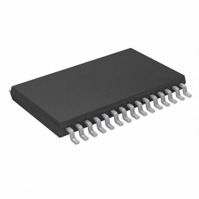
| 描述 | IC RECEIVER QWIKRADIO 16-QSOP射频接收器 QwikRadio Receiver (Not Recommended for New Designs) |
| 产品分类 | |
| 品牌 | Micrel |
| 产品手册 | |
| 产品图片 |
|
| rohs | 符合RoHS无铅 / 符合限制有害物质指令(RoHS)规范要求 |
| 产品系列 | RF集成电路,射频接收器,Micrel MICRF219AYQS- |
| 数据手册 | |
| 产品型号 | MICRF219AYQS |
| 产品目录页面 | |
| 产品种类 | 射频接收器 |
| 供应商器件封装 | 16-QSOP |
| 其它名称 | 576-3362-5 |
| 包装 | 管件 |
| 商标 | Micrel |
| 天线连接器 | PCB,表面贴装 |
| 存储容量 | - |
| 安装风格 | SMD/SMT |
| 封装 | Tube |
| 封装/外壳 | 16-SSOP(0.154",3.90mm 宽) |
| 封装/箱体 | QSOP-16 |
| 工作温度 | -40°C ~ 105°C |
| 工作电源电压 | 3.3 V |
| 工作频率 | 300 MHz to 450 MHz |
| 工厂包装数量 | 98 |
| 应用 | - |
| 数据接口 | PCB,表面贴装 |
| 数据速率(最大值) | 10 kbps |
| 最大工作温度 | + 105 C |
| 最小工作温度 | - 40 C |
| 标准包装 | 98 |
| 灵敏度 | -110dBm |
| 特性 | - |
| 电压-电源 | 3 V ~ 3.6 V |
| 电流-接收 | 6mA |
| 电源电压-最大 | 3.6 V |
| 电源电压-最小 | 3 V |
| 电源电流 | 4 mA |
| 类型 | ASK Receiver |
| 系列 | MICRF219 |
| 调制或协议 | ASK,OOK |
| 配用 | /product-detail/zh/ABM7-9.81563MHZ-10-R50-J4Q-T/535-10154-6-ND/2184281/product-detail/zh/ABM7-13.52127MHZ-10-R50-J4Q-T/535-10153-6-ND/2184280/product-detail/zh/ABLS-13.0625MHZ-10-K4Q-T/535-10149-6-ND/2184276/product-detail/zh/ABLS-13.52127MHZ-10-J-4Q-T/535-10148-6-ND/2184275/product-detail/zh/ABM7-9.81563MHZ-10-R50-J4Q-T/535-10154-1-ND/2184189/product-detail/zh/ABM7-13.52127MHZ-10-R50-J4Q-T/535-10153-1-ND/2184188/product-detail/zh/ABLS-13.0625MHZ-10-K4Q-T/535-10149-1-ND/2184184/product-detail/zh/ABLS-13.52127MHZ-10-J-4Q-T/535-10148-1-ND/2184183/product-detail/zh/ABM7-9.81563MHZ-10-R50-J4Q-T/535-10154-2-ND/2184097/product-detail/zh/ABM7-13.52127MHZ-10-R50-J4Q-T/535-10153-2-ND/2184096/product-detail/zh/ABLS-13.02519MHZ-10-K4Q-T/535-10150-2-ND/2184093/product-detail/zh/ABLS-13.0625MHZ-10-K4Q-T/535-10149-2-ND/2184092/product-detail/zh/ABLS-13.52127MHZ-10-J-4Q-T/535-10148-2-ND/2184091 |
| 频率 | 300MHz ~ 450MHz |


- 商务部:美国ITC正式对集成电路等产品启动337调查
- 曝三星4nm工艺存在良率问题 高通将骁龙8 Gen1或转产台积电
- 太阳诱电将投资9.5亿元在常州建新厂生产MLCC 预计2023年完工
- 英特尔发布欧洲新工厂建设计划 深化IDM 2.0 战略
- 台积电先进制程称霸业界 有大客户加持明年业绩稳了
- 达到5530亿美元!SIA预计今年全球半导体销售额将创下新高
- 英特尔拟将自动驾驶子公司Mobileye上市 估值或超500亿美元
- 三星加码芯片和SET,合并消费电子和移动部门,撤换高东真等 CEO
- 三星电子宣布重大人事变动 还合并消费电子和移动部门
- 海关总署:前11个月进口集成电路产品价值2.52万亿元 增长14.8%


PDF Datasheet 数据手册内容提取
MICRF219 300MHz to 450MHz ASK Receiver with RSSI, Auto-Poll, Bit-Check and Squelch NOT RECOMMENDED REFER TO MICRF219A FOR NEW DESIGNS General Description Features The MICRF219 is a 300MHz to 450MHz super- • –110dBm sensitivity at 1kbps with 1% BER heterodyne, image-reject, RF receiver with Automatic • Supports data rates up to 10kbps at 433.92MHz Gain Control, OOK/ASK demodulator and analog RSSI • 25dB Image-Reject Mixer output. The device integrates Auto-Poll, Valid Bit-Check, Squelch, and Desense features. It only requires a • No IF Filter Required crystal and a minimum number of external components • 60dB Analog RSSI Output to implement. It is ideal for low-cost, low-power, RKE, • 3.0V to 3.6V Supply Voltage Range TPMS, and remote actuation applications. • 4.0mA supply current at 315MHz (continuous receive) The MICRF219 achieves −110dBm sensitivity at a data • 6.0mA supply current at 434MHz (continuous receive) rate of 1kbps (Manchester encoded). Four demodulator • 0.5uA supply current in Shutdown Mode filter bandwidths are selectable in binary steps from 1625Hz to 13kHz at 433MHz, allowing the device to • Optional Auto-Polling (sleep mode, current < 0.1mA) support data rates to 10kbps. The device operates from • Optional Valid Bit-Check in Auto-Poll Mode a supply voltage of 3.0V to 3.6V, and consumes 4.0mA • Optional Programmable 6dB to 42dB Desense of supply current at 315MHz and 6.0mA at 433.92MHz. • Optional Data Output Squelch until valid bits detected A shutdown mode reduces supply current to 0.5uA. The Auto-Polling feature allows the MICRF219 to sleep and • 16-pin QSOP Package (4.9mm x 6.0mm) poll for user defined periods, thus further reducing • −40°C to +105°C Temperature Range supply current. The Valid Bit-Check feature, when • 2kV HBM ESD Rating enabled in Auto-Poll mode, fully awakes the receiver • Evaluation board QR219BPF Available and sends bits to the microcontroller once a valid number of bits are detected. During normal operation an Ordering Information optional Squelch feature disables the data output until valid bits are detected. An optional Desense feature Part Number Temperature Range Package reduces gain by 6dB to 42dB, distancing the receiver MICRF219AYQS −40°C to +105°C 16-Pin QSOP from distantly placed, undesired transmitters. _______________________________________________________________________________________________ Typical Application QwikRadio is a registered trademark of Micrel, Inc. Micrel Inc. • 2180 Fortune Drive • San Jose, CA 95131 • USA • tel +1 (408) 944-0800 • fax + 1 (408) 474-1000 • http://www.micrel.com June 2011 M9999-060811 (408) 944-0800
Micrel MICRF219 Pin Configuration RO1 1 16 RO2 GNDRF 2 15 SCLK ANT 3 14 RSSI GNDRF 4 13 CAGC Vdd 5 12 CTH SQ 6 11 SEL1 SEL0 7 10 DO SHDN 8 9 GND MICRF219AYQS Pin Description 16-Pin Pin Name Pin Function QSOP Reference Oscillator Input: Reference resonator input connection to pierce oscillator stage. May also 1 RO1 be driven by external reference signal of 200mVp-p to 1.5V p-p amplitude maximum. Internal capacitance of 7pF to GND during normal operation. 2 GNDRF Negative supply connection associated with ANT RF input. Antenna Input: RF signal input from antenna. Internally AC coupled. It is recommended a matching 3 ANT network with an inductor-to-RF ground be used to improve ESD protection. 4 GNDRF Ground connection for ANT RF input. Positive supply connection for all chip functions. Bypass with 0.1µF capacitor located as close to the 5 VDD VDD pin as possible. Squelch Control Logic-Level Input. An internal pull-up pulls the logic-input HIGH when the device is 6 SQ enabled. Bit D17 sets whether squelch is enabled or disabled when a logic-level signal is applied the SQ pin. See Squelch Enable Truth-Table on page Demodulator Filter Bandwidth Select Logic-Level Input. Internal pull-up (3uA typical) when not in 7 SEL0 shutdown or SLEEP mode. Used in conjunction with SEL1 to control D3 bandwidth LSB when serial interface contains default setting. It does not need to be defined in SLEEP mode. Shutdown control Logic-Level Input. A logic-level LOW enables the device. A logic-level HIGH places 8 SHDN the device in low-power shutdown mode. An internal pull-up pulls the logic input HIGH. 9 GND Negative supply connection for all chip functions except for RF input. Data Input and Output. Demodulated data output. May be blanked until bit checking test is acceptable. 10 DO A current limited CMOS output during normal operation this pin is also used as a CMOS Schmitt input for serial interface data. A 25kΩ pull-down is present when device is in shutdown and sleep modes. Demodulator Filter Bandwidth Select Logic-Level Input: Internal (3uA typical) pull-up when not in 11 SEL1 shutdown or SLEEP mode. Used in conjunction with SEL0, to control D4 bandwidth MSB, when serial interface contains default setting. It does not need to be defined in SLEEP mode. Demodulation threshold voltage integration capacitor. Capacitor-to-GND sets the settling time for the 12 CTH demodulation data slicing level. Values above 1nF are recommended and should be optimized for data rate and data profile. 13 CAGC AGC filter capacitor. A capacitor, normally greater than 0.47μF, is connected from this pin-to-GND Received signal strength indication (output): Output is from a switched capacitor integrating op amp 14 RSSI with 220Ω typical output impedance. Serial interface input clock. CMOS Schmitt input. A 25kΩ pull-down is present when device is in 15 SCLK shutdown mode. 16 RO2 Reference resonator connection. Internal capacitance of 7pF to GND during normal operation. June 2011 2 M9999-060811 (408) 944-0800
Micrel MICRF219 Absolute Maximum Ratings(1) Operating Ratings(2) Supply Voltage (VDD)................................................+5V Supply voltage (VDD).............................+3.0V to +3.6V Input Voltage..............................................................+5V Ambient Temperature (T ).................–40°C to +105°C A Junction Temperature...........................................+150ºC Input Voltage (Vin).................................................3.6V Lead Temperature (soldering, 10sec.)....................300°C Maximum Input RF Power................................−20dBm Storage Temperature (Ts)......................-65ºC to +150°C Receive Modulation Duty Cycle(6)....................20~80% Maximum Receiver Input Power.........................+10dBm Frequency Range...........................300MHz to 450MHz EDS Rating(3)...................................................2KV HBM Electrical Characteristics Specifications apply for VDD = 3.3V, GND = 0V, CAGC = 4.7µF, CTH = 0.1µF, fRX = 433.92 MHz unless otherwise noted. Bold values indicate –40°C – TA – 105°C. 1kbps data rate (Manchester encoded), reference oscillator frequency = 13.52127MHz. Parameter Condition Min. Typ. Max. Units Continuous Operation, f = 315MHz 4.0 RX Operating Supply Current mA Continuous Operation, f = 433.92MHz 6.0 RX Shutdown Current 0.15 µA Receiver Image Rejection 25 dB f = 315MHz 0.86 1st IF Center Frequency RX MHz f = 433.92MHz 1.2 RX Receiver Sensitivity @ 1kbps fRX = 315 MHz, 50Ω BER=10-2 −110 dBm (Note 4) fRX = 433.92MHz, 50Ω BER=10-2 −110 f = 315MHz 235 RX IF Bandwidth kHz f = 433.92MHz 330 RX f = 315MHz 32 – j235 RX Antenna Input Impedance Ω f = 433.92MHz 19 – j174 RX Receive Modulation Duty Cycle Note 5 20 80 % AGC Attack / Decay Ratio t / t 0.1 ATTACK DECAY TA = 25ºC ±30 nA AGC Pin Leakage Current TA = +105ºC ±800 nA RF @ −40dBm 1.15 V IN AGC Dynamic Range RF @ −100dBm 1.70 V IN Reference Oscillator f = 315 MHz, Crystal Load Cap = 10pF 9.81563 RX Reference Oscillator Frequency MHz f = 433.92 MHz, Crystal Load Cap = 10pF 13.52127 RX Reference Oscillator Input RO1 1.6 kΩ Impedance Reference Oscillator Bias Voltage RO2 1.15 V June 2011 3 M9999-060811 (408) 944-0800
Micrel MICRF219 Electrical Characteristics (Continued) Specifications apply for V = 3.3V, GND = 0V, C = 4.7µF, C = 0.1µF, f = 433.92 MHz unless otherwise noted. Bold values DD AGC TH RX indicate –40°C – T – 105°C. 1kbps data rate (Manchester encoded), reference oscillator frequency = 13.52127MHz. A Parameter Condition Min. Typ. Max. Units Reference Oscillator Input Range 0.2 1.5 V P-P Reference Oscillator Source V(REFOSC) = 0V 300 µA Current Demodulator F = 9.81563 MHz 165 REFOSC CTH Source Impedance kΩ F = 13.52127MHz 120 REFOSC T = 25ºC ±2 CTH Leakage Current A nA TA = +105ºC ±800 Demodulator Filter Bandwidth Programmable, see application section 1170 9400 Hz @ 315MHz Demodulator Filter Bandwidth Programmable, see application section 1625 13000 Hz @ 434MHz Digital / Control Functions As output source @ 0.8 V 260 DO Pin Output Current DD µA sink @ 0.2 V 600 DD Output Rise And Fall Times CI = 15pF, pin DO, 10-90% 2 µsec Pins SCLK, DO (As input), SHDN,SEL0, Input High Voltage 0.8V V SEL1,SQ DD Pins SCLK, DO (As input), SHDN, SEL0, Input Low Voltage 0.2V V SEL1,SQ DD Output Voltage High DO 0.8V V DD Output Voltage Low DO 0.2V V DD RSSI −100dBm 0.4 RSSI DC Output Voltage Range V −40dBm 2.0 RSSI Response Slope −110dBm to -40dBm 25 mV/dB RSSI Output Current 400 µA RSSI Output Impedance 250 Ω 50% data duty cycle, input power to Antenna = - RSSI Response Time 0.3 sec 20dBm Notes: 1. Exceeding the absolute maximum rating may damage the device. 2. The device is not guaranteed to function outside of its operating rating. 3. Device is ESD sensitive. Use appropriate ESD precautions. Exceeding the absolute maximum rating may damage the device. 4. Sensitivity is defined as the average signal level measured at the input necessary to achieve 10-2 BER (bit error rate). The input signal is defined as a return-to-zero (RZ) waveform with 50% average duty cycle (Manchester encoded) at a data rate of 1kbps. 5. When data burst does not contain preamble, duty cycle is defined as total duty cycle, including any “quiet” time between data bursts. When data bursts contain preamble sufficient to charge the slice level on capacitor C , then duty cycle is the effective duty cycle of the burst alone. [For TH example, 100msec burst with 50% duty cycle, and 100msec “quiet” time between bursts. If burst includes preamble, duty cycle is T /(T +t )= 50%; without preamble, duty cycle is T /(T + T + T ) = 50msec/(200msec)=25%. T is the (Average number of ON ON OFF ON ON OFF QUIET ON 1’s/burst) × bit time, and T = (T – T .) OFF BURST ON June 2011 4 M9999-060811 (408) 944-0800
Micrel MICRF219 Typical Characteristics 433MHz Selectivity and Bandwidth by Different Temps. -50 -60 m) B -70 d Y ( -80 T VI TI -90 C LE-100 -40°C E +105°C S -110 +20°C -120 9 1 3 5 7 9 1 3 5 7 9 2. 3. 3. 3. 3. 3. 4. 4. 4. 4. 4. 3 3 3 3 3 3 3 3 3 3 3 4 4 4 4 4 4 4 4 4 4 4 FREQUENCY (MHz) 433.92MHz V/I by Temperatures 7 105°C 6.5 mA) 6 20°C T ( N5.5 E -40°C R R U 5 C 4.5 4 3.0 3.1 3.2 3.3 3.4 3.5 3.6 VOLTAGE (V) June 2011 5 M9999-060811 (408) 944-0800
Micrel MICRF219 Functional Diagram CAGC DOWNCUOHVFERTER COLONTGRICOL DESENSE COANGTCROL MIXER LNA -f f IF AMP DETECTOR RSSI RSSI MIXER i fLO RFIMEILJATEGECERT COLONTGRICOL PROGRAMMABLE DEMOODOUKLATOR FILTER SYNTHESIZER SLICER DO' BITCHECK SLEEP SLEEP DO OSCILLATOR TIMER WAKE-UP SQUELCH CTH AUTOPOLL SLICE DO' CONTROL LEVEL DO LOGIC ORSECFEILRLEANTOCRE COLONTGRICOL REFERENCE AND CONTROL Figure 1. Simplified Block Diagram June 2011 6 M9999-060811 (408) 944-0800
Micrel MICRF219 Functional Description The IF BW can be calculated via direct scaling: The simplified block diagram, shown in Figure 1, illustrates the basic structure of the MICRF219 receiver. BWIF = BWIF@433.92 MHz × It is made up of four sub-blocks: ⎛Operating Freq (MHz)⎞ ⎜ ⎟ • UHF Down-converter ⎝ 433.92 ⎠ • OOK Demodulator • Reference and Control logic These filters are fully integrated inside the MICRF219. • Auto-poll circuitry After filtering, four active gain controlled amplifier stages enhance the IF signal to its proper level for Outside the device, the MICRF219 receiver requires just demodulation. three components to operate: two capacitors (CTH, and OOK Demodulator CAGC) and the reference frequency device (usually a quartz crystal). An additional five components are used The demodulator section is comprised of detector, to improve performance; a power supply decoupling programmable low pass filter, slicer, and AGC capacitor, two components for the matching network, comparator. and two components for the pre-selector band-pass filter. Detector and Programmable Low-Pass Filter The demodulation starts with the detector removing the Receiver Operation carrier from the IF signal. Post detection, the signal becomes base band information. The programmable UHF Downconverter low-pass filter further enhances the baseband The UHF down-converter has six components: LNA, information. There are four programmable low-pass mixers, synthesizer, image reject filter, band pass filter filter BW settings: 1625Hz, 3250Hz, 6500Hz, 13000Hz and IF amp. for 433.92MHz operation. Low pass filter BW will vary with RF Operating Frequency. Filter BW values can be LNA easily calculated by direct scaling. See equation below The RF input signal is AC-coupled into the gate circuit of for filter BW calculation: the grounded source LNA input stage. The LNA is a Cascoded NMOS amplifier. The amplified RF signal is then fed to the RF ports of two double balanced mixers. ⎛Operating Freq (MHz)⎞ BW = BW * ⎜ ⎟ Operating Freq @433.92MHz ⎝ 433.92 ⎠ Mixers and Synthesizer The LO ports of the Mixers are driven by quadrature local oscillator outputs from the synthesizer block. The It is very important to choose filter setting that fits best local oscillator signal from the synthesizer is placed on the intended data rate to minimize data distortion. the low side of the desired RF signal to allow Demod BW is set at 13000Hz @ 433.92MHz as default suppression of the image frequency at twice the IF (assuming both SEL0 and SEL1 pins are floating). The frequency below the wanted signal. The local oscillator low pass filter can be hardware set by external pins is set to 32 times the crystal reference frequency via a SEL0 and SEL1. phase-locked loop synthesizer with a fully integrated loop filter. SEL0 SEL1 Demod BW (@ 434MHz) Image-Reject Filter and Band-Pass Filter 0 0 1625Hz The IF ports of the mixer produce quadrature-down 1 0 3250Hz converted IF signals. These IF signals are low-pass 0 1 6500Hz filtered to remove higher frequency products prior to the image reject filter where they are combined to reject the 1 1 13000Hz - default image frequencies. The IF signal then passes through a third order band pass filter. The IF center frequency is Table 1. Demodulation BW Selection 1.2MHz. The IF BW is 330kHz @ 433.92MHz. This varies with RF operating frequency. June 2011 7 M9999-060811 (408) 944-0800
Micrel MICRF219 The de-sense function is accessible only through serial Slicer and Slicing Level programming. The signal, prior to the slicer, is still AM. The data slicer converts the AM signal into ones and zeros based on the threshold voltage built up in the CTH capacitor. D0 D1 D2 MODE: Desense After the slicer, the signal is ASK or OOK digital data. 0 X X No Desense - default The slicing threshold is default at 50%. The slicing 1 0 0 6dB Desense threshold can be set via serial programming through 1 1 0 16dB Desense register D5 and D6. 1 0 1 30dB Desense 1 1 1 42dB Desense D5 D6 Slicing Level 1 0 Slice Level 30% Reference Control 0 1 Slice Level 40% There are 2 components in Reference and Control sub- block: 1) Reference Oscillator and 2) Control Logic 1 1 Slice Level 50% - default through parallel Inputs: SEL0, SEL1, SHDN 0 0 Slice Level 60% Reference Oscillator AGC Comparator The reference oscillator in the MICRF219 (Figure 2) The AGC comparator monitors the signal amplitude uses a basic Pierce crystal oscillator configuration with from the output of the programmable low-pass filter. MOS transconductor to provide negative resistance. When the output signal is less than 750mV thresh-hold, Though the MICRF219 has build-in load capacitors for 1.5µA current is sourced into the external CAGC the crystal oscillator, the external load capacitors are still capacitor. When the output signal is greater than required for tuning it to the right frequency. R01 and R02 750mV, a 15µA current sink discharges the CAGC are external pins of the MICRF219 to connect the crystal capacitor. The voltage developed on the CAGC to the reference oscillator. capacitor acts to adjust the gain of the mixer and the IF Reference oscillator crystal frequency can be calculated: amplifier to compensate for RF input signal level variation. F = F /(32 + 1.1/12) Desense REF OSC RF Desense is a function designed to reduce the sensitivity For 433.92 MHz, F = 13.52127 MHz. of the MICRF219 receiver to a maximum of 45dB for REF OSC training the MICRF219 receiver. This is done in order to recognize an intended transmitter. Very often, a receiver To operate the MICRF219 with minimum offset, crystal needs to learn how to recognize a particular transmitter. frequencies should be specified with 10pF loading It is important for the receiver not to learn the signal of a capacitance. stray transmitter near by. The simplest solution is to turn down the receiver gain, so the receiver only recognizes the transmitter at close range. June 2011 8 M9999-060811 (408) 944-0800
Micrel MICRF219 RO2 C V BIAS R RO1 C Figure 2. Reference Oscillator Circuit SQUELCH Decode <=4 Data Edge Pulses S Q Good CLK 8 Stage SQUELCH DOUT Shift Register Disables DO Edge D Detector Window >=7 CLK Counter R Good CLK Decode Decode Good Bad Bits Bit Count Window Decode Good Bit QA1 Bad Bit Returns to D7 D8 SLEEP Select 0, 2, 4, 8 Good CLK Bits BeforeWakeup WATCHDOG Timer Auto Poll WAKEUP Timer (300µs) S R D15 = 0 for Normal Operation Serial Control Register D15 D15 = 1 forAuto Polled Operation Figure 3. Autopoll, Bit-Check Block Diagram June 2011 9 M9999-060811 (408) 944-0800
Micrel MICRF219 Auto-Polling The auto-poll block (Figure 3) contains a low power that a window time set longer than this will result in all oscillator that drives the sleep timer when the rest of bits being tested as bad and the device will remain in the device is powered down. It also contains circuits to sleep polling mode. Now, when the serial command check whether the received bits are good. Auto- sets bit D15 high, the device will go to sleep for the polling is controlled by bit D15 in the serial register, in timer period and will then awake to receive and check conjunction with bits D12, D13, D14 to set the sleep bits. The device will output data again at DO as soon timer period. Bits D7, D8, are used for control of the as the programmed numbers of good RTZ bits have bit-check operation and bits D9, D10, D11 are used to been received. If a bad bit is seen, the device will adjust the sensitivity of the bit-check action. return to sleep mode and poll again for good bits after the sleep period. Both high and low periods are Auto-Polling without Bit-Checking checked for each RTZ bit. The device will continue to For simple auto-polling without bit-checking, send a check bits until sufficient good bits enable the device serial command with bit D15 set high and bits D12, to wake up, or bad bits return the device to sleep. D13, D14 set to the desired sleep time. The device will go to sleep for the programmed timer duration Operation then wake up to receive data if it is present. The Received pulse edges trigger a programmable device will stay awake until serial bit D15 is set low, window timer clocked by the reference frequency. If then set high again, to enable a further sleep period. the next pulse edge falls within this window the bit is The sleep duty cycle may be controlled by the timing flagged as bad. Detected good bits are counted and of serial commands. the device will wake up once sufficient pulses have been received. Two bad pulses or a lack of pulses will Auto-Polling with Bit-Checking cause the device to go to sleep for a further sleep For auto-polling with bit-checking, the serial register timeout period. bits D7and D8 need to be set for the number of bits to be checked as good, before the receiver outputs data Squelch at the DO pin. The bit-check window bits D9, D10, During normal operation, if four or less out of eight bit D11 must also be set to match the data period. The pulses are good, the DO output is squelched. If good shortest default window time gives the least critical bit bit count increases to seven or more in any eight check action. For better discrimination, the window sequential bits, squelch is disabled allowing data to setting may be increased up towards the normal output at DO pin. minimum time expected between data edges. Note June 2011 10 M9999-060811 (408) 944-0800
Micrel MICRF219 Serial Interface Register Programming Default State D9, D10, D11 is 111 Control Register Individual Truth Tables: MODE: D12 D13 D14 D0 D1 D2 MODE: Desense Sleep Time 0 X X No Desense - default 0 0 0 10ms 1 0 0 6dB Desense 1 0 0 20ms 1 1 0 16dB Desense 0 1 0 40ms Default 1 0 1 30dB Desense 1 1 0 80ms 1 1 1 42dB Desense 0 0 1 160ms 1 0 1 320ms 0 1 1 640ms MODE: D3 D4 1 1 1 1280ms Demod Bandwidth (at 433.92MHz) 0 0 1625Hz 1 0 3250Hz D15 MODE: Auto-Poll 0 1 6500Hz 0 Awake – does not poll - default 1 1 13000Hz - default 1 Auto-polls with Sleep periods D5 D6 MODE D16 Always Set This Bit to 0 1 0 Slice Level 30% 0 1 Slice Level 40% SQ Pin D17 MODE: Squelch Enable 1 1 Slice Level 50% - default 0 0 Squelch Circuit Enabled 0 0 Slice Level 60% 0 1 Squelch Circuit Disabled 1 0 Squelch Circuit Disabled (default) D7 D8 MODE: Bit-Check Setting 1 1 Squelch Circuit Enabled 0 0 Bit-check 0 bits - default 1 0 Bit-check 2 bits The external pin SQ can invert the setting of squelch 0 1 Bit-check 4 bits on/off defined by register bit D17. The external pin 1 1 Bit-check 8 bits defaults high via an internal pull-up so the squelch is off with default D17 = 0 and on if D17 = 1. Such bit MODE: logic is reversed if SQ pin is tied to low (Ground). D9 D10 D11 Bit-Check Window Times (315 MHz) Set D3 to D3=1 D3=0 D3=1 D3=0 D18 Always Set This Bit to 1 Set D4 to D4=1 D4=1 D4=0 D4=0 0 0 0 98us, 196us, 393us, 785us 1 0 0 92us, 183us, 367us, 733us D19 Always Set This Bit to 0 0 1 0 85us, 170us, 341us, 681us 1 1 0 79us, 157us, 314us, 629us 0 0 1 72us, 144us, 288us, 577us 1 0 1 66us, 131us, 262us, 525us 0 1 1 59us, 118us, 236us, 473us 1 1 1 53us, 105us, 210us, 420us MODE: D9 D10 D11 Bit-Check Window Times (433.92MHz) Set D3 to D3=1 D3=0 D3=1 D3=0 Set D4 to D4=1 D4=1 D4=0 D4=0 0 0 0 71us, 143us, 285us, 570us 1 0 0 67us, 133us, 266us, 532us 0 1 0 62us, 124us, 247us, 494us 1 1 0 57us, 114us, 228us, 457us 0 0 1 52us, 105us, 209us, 419us 1 0 1 48us, 95us, 190us, 381us 0 1 1 43us, 86us, 172us, 343us 1 1 1 38us, 76us, 152us, 305us June 2011 11 M9999-060811 (408) 944-0800
Micrel MICRF219 Application Information Figure 4. QR219BPF Application Example, 433.92MHz Table 2 shows the component values for most often Antenna and RF Port Connections used frequencies. Figure 4 shows the schematic of the QR219BPF configured for 433.29 MHz operation. Figure 19 through Figure 23 are PCB pictures. The QR219BPF Freq (MHz) C8 (pF) L1 (nH) is a good starting point for the prototyping of most 315.0 6.8 39 applications. Current design offers two antenna 390.0 6.8 24 options: A wire antenna or 50Ω SMA antenna. The 418.0 6.0 24 SMA connection also allows an RF signal to be 433.92 5.6 24 injected for test or verification. To use an antenna such as a 50 Ω whip, remove the SMA and solder the whip antenna in the hole on the PCB instead. A wire Table 2. Front Band-Pass Filter values for Various of 22AWG with 167mm (6.-inch) can be used as a Frequencies substitution if low cost antenna is needed. This band-pass filter can be removed if the outside Front-End Band Pass Filter band noise does not cause a problem. The MICRF219 Components L1 and C8 form the band-pass filter at has built-in image reject mixers which improve the front of the receiver. Its purpose is to attenuate selectivity significantly and reject outside band noise. undesired outside band noise that degrades the receiver performance. It is calculated by the parallel resonance equation: f = 1/(2×PI×(SQRT L1×C8)) June 2011 12 M9999-060811 (408) 944-0800
Micrel MICRF219 Doing the same calculation example with the Smith Low-Noise Amplifier Input Matching Chart, would appear as follows, Capacitor C3 and inductor L2 form the “L” shape input First, one plots the input impedance of the device, matching network. The capacitor provides additional (Z = 18.6 – j174.2)Ω @ 433.92MHz.(Figure 5): attenuation for low-frequency outside band noise. The inductor provides additional ESD protection for the antenna pin. Two methods can be used to find these values that best matched near 50Ω. One method is done by calculating the values using the equations below and the other is using a Smith chart utility. The latter is made easier via a software plot where components are added on. In this way, the user can see the impedance moving direction for best values of C8 and L1 toward to central matching point, like WinSmith by Noble Publishing. To calculate the matching values, one needs to know the input impedance of the device. Table 3 shows the input impedance of the MICRF219 and suggested matching values for the most often used frequencies. These suggested values may be different if the layout is not exactly the same as the one made here: Freq (MHz) C3 (pF) L2(nH) Z device (Ω) 315 1.8 68 33 - j235 390 1.5 47 23 – j199 418 1.5 43 21 – j186 433.92 1.5 39 19 – j174 Figure 5. Device’s Input Impedance, Z = 19 – j174Ω Table 3. Matching Values for the Most Used Second, one plots the shunt inductor (39nH) and the Frequencies series capacitor (1.5pF) for the desired input impedance (Figure 6). One can then see the matching For the frequency of 433.92MHz, the input impedance leading to the center of the Smith Chart or close to is Z = 18.6 – j174.2Ω, then the matching components 50Ω. are calculated by: Equivalent parallel = B = 1/Z = 0.606 + j5.68msiemens Rp = 1 / Re (B); Xp = 1 / Im (B) Rp = 1.65kΩ; Xp = 176.2Ω Q = SQRT (Rp/50 + 1) Q = 5.831 Xm = Rp / Q Xm = 282.98Ω Resonance Method for L-shape Matching Network Lc = Xp / (2×Pi×f); Lp = Xm / (2×Pi×f) L2 = (Lc×Lp) / (Lc + Lp); C3 = 1 / (2×Pi×f×Xm) L2 = 39.8nH C3 = 1.3pF June 2011 13 M9999-060811 (408) 944-0800
Micrel MICRF219 Crystal Selection Crystal Y1 or Y1A (SMT or leaded respectively) is the reference clock for all the device internal circuits. Crystal characteristics of 10pF load capacitance, 30ppm, ESR < 50Ω, −40ºC to +105ºC temperature range are desired. Table 4 shows Micrel’s approved crystal suppliers such as (www.hib.com.br or http://www.abracon.com/ ) and the frequencies. The oscillator of the MICRF219 is a Pierce-type oscillator. Good care must be taken when laying out the printed circuit board. Avoid long traces and place the ground plane on the top layer close to the REFOSC pins RO1 and RO2. When care is not taken in the layout, and the crystals used are not verified, the oscillator may take longer time to start. Time-to- good-data in the DO pin will be longer as well. In some cases, if the stray capacitance is too high (> 20pF). In this case, either the receiving central frequency will offset too much or the oscillator may not start. The crystal frequency is calculated by REFOSC = RF Carrier/(32+(1.1/12)). The local oscillator is low-side injection (32 × 13.52127MHz = 432.68MHz), that is, its frequency is below the RF carrier frequency and the image frequency is below the LO frequency. See Figure 7. The product of the incoming RF signal and local oscillator signal will yield the IF frequency, which will be demodulated by the detector of the device. Figure 7. Low-Side Injection Local Oscillator Figure 6. Plotting of Shunt Inductor and Series Capacitor June 2011 14 M9999-060811 (408) 944-0800
Micrel MICRF219 REFOSC (MHz) Carrier (MHz) HIB Part Number Abracon Part Number 9.81563 315.0 SA-9.815630-F-10-H-30-30-X ABLS-9.81563MHz-10J4Y 12.15269 390.0 SA-12.152690-F-10-H-30-30-X ABLS-12.15269MHz-10J4Y 13.02519 418.0 SA-13.025190-F-10-H-30-30-X ABLS-13.025190MHz-10J4Y 13.52127 433.92 SA-13.521270-F-10-H-30-30-X ABLS-13.521270MHz-10J4Y Table 4. Crystal Frequencies and Vendor Part Numbers Demodulator Bandwidth Selection and Data Stream Optimization JP1 and JP2 are the bandwidth selection for the Maximum demodulator bandwidth. To set it correctly, it is Demod. Shortest Baud Rate SEL0 SEL1 necessary to know the shortest pulse width of the JP1 JP2 BW Pulse for 50% encoded data sent in the transmitter. Similar to the (hertz) (µsec) Duty Cycle (Hz) example of the data profile in the Figure 7, PW2 is shorter than PW1, so PW2 should be used for the Short Short 1565 416 1204 demodulator bandwidth calculation which is found by Open Short 3130 208 2408 0.65/shortest pulse width. After this value is found, the Short Open 6261 104 4816 setting should be done according to Table 5. For Open Open 12523 52 9633 example, if the pulse period is 100µsec, 50% duty cycle, the pulse width will be 50µsec (PW = (100µsec × 50%) / 100). Therefore, a bandwidth of 13kHz would Table 6. P1 and JP2 Setting, 418.0MHz be necessary (0.65 / 50µsec). However, if this data stream had a pulse period with a 20% duty cycle, then the bandwidth required would be 32.5kHz (0.65 / Maximum 20µsec). This would exceed the maximum bandwidth Demod. Shortest Baud Rate of the demodulator circuit. If one tries to exceed the SEL0 SEL1 BW Pulse for 50% maximum bandwidth, the pulse would appear JP1 JP2 (hertz) (µsec) Duty Cycle stretched or wider. (Hz) Short Short 1170 445 1123 Demod. Shortest Maximum Open Short 2350 223 2246 SEL0 SEL1 Baud Rate JP1 JP2 BW Pulse for 50% Duty Short Open 4700 111 4493 (hertz) (µsec) Cycle (Hz) Open Open 9400 56 8987 Short Short 1625 400 1250 Open Short 3250 200 2500 Table 7. JP1 and JP2 Setting, 315MHz Short Open 6500 100 5000 AGC Capacitor and Data Slicer Threshold Open Open 13000 50 10000 Capacitor Selection Capacitors C6 and C4 are C and C capacitors Table 5. JP1 and JP2 Setting, 433.92MHz TH AGC respectively providing a time base reference for the data pattern received. These capacitors are selected Other frequencies will have different demodulator according to data profile, pulse duty cycle, dead time bandwidth limits, which is derived from the reference between two received data packets, and if the data oscillator frequency. Table 6 and Table 7 shows the pattern does has or not have a preamble. See Figure limits for the other two most used frequencies. 8 for example of a data profile. June 2011 15 M9999-060811 (408) 944-0800
Micrel MICRF219 Figure 8. Example of a Data Profile For best results, they should always be optimized for the data pattern used. As the baud rate increases, the capacitor values decrease. Table 8 shows suggested values for Manchester Encoded data, 50% duty cycle. Demod. Figure 9. Data Out Pin with No Squelch (SQ = 1) SEL0 SEL1 BW Cth Cagc JP1 JP2 (Hz) Short Short 1625 100nF 4.7µF Open Short 3250 47nF 2.2µF Short Open 6500 22nF 1µF Open Open 13000 10nF 0.47µF Table 8. Suggested C and C Values TH AGC JP3 and JP4 are jumpers selectable to high or low and used to configure the digital squelch function. When it is tied to high, there is no squelch applied to the digital circuits and the DO (data out) pin has a hash signal. When the pin is low, the DO pin activity is considerably reduced. It will have more or less than shown in the figure below depending upon the outside band noise. The penalty for using squelch is a delay in getting a good signal in the DO pin. This means that it takes longer for the data to show up. The delay is Figure 10. Data Out Pin with Squelch (SQ = 0) dependent upon many factors such as RF signal intensity, data profile, data rate, C and C Other components used are C5, which is a decoupling TH AGC capacitor values, and outside band noise See Figure capacitor for the V line; R3 for the shutdown pin DD 9 and Figure 10. Please note that Squelch action is (SHDN = 0, device is operation), which can be based on the Bitcheck operation and may be removed if that pin is connected to a microcontroller or optimized using the Bitcheck Window serial register an external switch; and R1 and R2 which form a setting. voltage divider for the AGC pin. One can force a voltage in this AGC pin to purposely decrease the device sensitivity. Special care is needed when doing this operation, as an external control of the AGC voltage may vary from lot to lot and may not work the same in several devices. June 2011 16 M9999-060811 (408) 944-0800
Micrel MICRF219 Three other pins are worthy of comment. They are the DO, RSSI, and shutdown pins. The DO pin has a driving capability of 0.4mA. This is good enough for most of the logic family ICs on the market today. The RSSI pin provides a transfer function of the RF signal intensity versus voltage. It is very useful to determine the signal-to-noise ratio of the RF link, crude range estimate from the transmitter source and AM demodulation, which requires a low C capacitor AGC value. The shutdown pin (SHDN) is useful to save energy. Making its level close to V (SHDN = 1), the device is DD not in operation. Its DC current consumption is less than 1µA (do not forget to remove R3). When toggling from high to low, there will be a time required for the device to come to steady-state mode, and a time for data to show up in the DO pin. This time will be Figure 12. Time-to-Good-Data after Shutdown Cycle, dependent upon many things such as temperature, 315MHz at Room Temperature the crystal used, and if there is an external oscillator with faster startup time. See Figure 11 and Figure 12 Serial Register Programming or time-to-good-data on both 433.92MHz and 315MHz Programming the device is accomplished by the use versions. of pins DO and SCLK. Normally, D0 (Pin 10) is outputting data and needs to switch to an input pin made by the start sequence, as shown at Figure 13. High at the SCLK pin tri-states the DO pin, enabling the external drive into the DO pin with an initial low level. The start sequence is completed by taking SCLK low, then high while DO is low, followed by taking DO high, then low while SCLK is high. The serial interface is initialized and ready to receive the programming data. T6 T7 BITTIME0 BIT TIME1 BITTIME2 SCLK T1 T2 T4 T5 T8 T9 T3 “19” “0” “0” “1” DO AS DO INPUT BITS: D19 D18 D17 OUTPUT Figure 11. Time-to-Good-Data after Shutdown Cycle, Figure 13. Serial Interface Start Sequence 433.92MHz, Room Temperature June 2011 17 M9999-060811 (408) 944-0800
Micrel MICRF219 Bits are serially programmed starting with the most Serial Interface Register Loading Examples significant bit (MSB = D19) if all bits are being programmed until the least significant bit (LSB =D0) See Figures 15 – 17. (Channel 1 is the DO pin, and For instance, if only the desense bits D0, D1, and D2 channel 2 is the SCLK pin). are being programmed, then these are the only bits that need to be programmed with the start sequence D2, D1, D0, plus the stop sequence. Or, if only the squelch bit D17 is needed, then the sequence must be from start sequence, D17 through D0 plus the stop sequence, making sure the other bits (besides D17) are programmed as needed. It is recommended that all parallel input pins (SEL0, SEL1, and SQ) be kept high when using the serial interface. After the programming bits are finished, a stop sequence (as shown in Figure 14) is required to end the mode and reestablish the DO pin as an output again. To do so, the SCLK pin is kept high while the DO pin changes from low to high, then low again, followed by the SCLK pin made low. Timing of the programming bits are not critical, but should be kept as shown below: T1 < 0.1µs, Time from SCLK to convert DO to input pin Figure 15. All Bits D19 through D0 = 0 T6 > 0.1µs, SCLK high time T7 > 0.1µs, SCLK low time T2, T3, T4, T5, T8, T9, T10 > 0.1µs BIT TIME 18 BIT TIME 19 SCLK T10 “1” “0” “1” DO D1 DO DO PIN AS OUTPUT Figure 14. Serial Interface Stop Sequence SCLK frequency should be greater than 5kHz to avoid automatic reset from internal circuitry. Figure 16. All Bits D19 through D0 = 1 June 2011 18 M9999-060811 (408) 944-0800
Micrel MICRF219 From MSB to LSB (see Table 9): D19 D18 D17 D16 D15 D14 D13 D12 0 1 0 0 1 1 0 0 D11 D10 D9 D8 D7 D6 D5 0 1 1 1 0 1 1 D4 D3 D2 D1 D0 0 0 0 0 0 Table 9. Auto-Poll Example Bit Sequence Figure 17. D19 = D18 = 1, D17 = D0 = 0 Auto-Poll Programming Example Auto-Poll example (see Figure 18): D0 = D1 = D2 = 0, no desense D3 = D4 = 0, demodulator bandwidth = 1712 hertz, 1 kHz baud rate, pulse = 500µsec. Required demodulator bandwidth is 0.65/500usec = 1300 hertz D5 = D6 = 1, Slice level = 50% D7 = 0, D8 = 1, bit check = 4 bits. This is the time the device is ON checking for four consecutive valid windows. Figure 18. Autopoll Example D9 = D10 = 1, D11 = 0, data rate is 1 kHz, (500µsec pulses), window set to 433µsec (< 500 usec) D12 = D13 = 0, D14 = 1, sleep timer set to 160msec, that is, 4 bit is ON and 160msec is OFF. D15 = 1, device is placed in autopoll D16 = 0, not used. Always set to 0. D17 = 0, squelch is OFF D18 = 1, watchdog timer is OFF D19 = 0, no RSSI offset June 2011 19 M9999-060811 (408) 944-0800
Micrel MICRF219 PCB Considerations and Layout inductance. Ground plane should be solid and with no sudden interruptions. Avoid using ground plane on top Figure 19 to Figure 23 show the QR219BPF PCB layer next to the matching elements. It normally adds layout. The Gerber files provided are downloadable additional stray capacitance which changes the from Micrel Website and contain the remaining layers matching. Do not use Phenolic materials as they are needed to fabricate this board. When copying or conductive above 200MHz. Typically, FR4 or better making one’s own boards, make the traces as short materials are recommended. The RF path should be as possible. Long traces alter the matching network as straight as possible to avoid loops and and the values suggested are no longer valid. unnecessary turns. Separate ground and V lines DD Suggested matching values may vary due to PCB from other digital or switching power circuits (such variations. A PCB trace 100 mills (2.5mm) long has microcontroller…etc). Known sources of noise should about 1.1nH inductance. Optimization should always be laid out as far as possible from the RF circuits. be done with exhaustive range tests. Make sure the Avoid unnecessary wide traces which would add more individual ground connection has a dedicated via distribution capacitance (between top trace to bottom rather then sharing a few of ground points by a single GND plane) and alter the RF parameters. via. Sharing ground via will increase the ground path Figure 19. QR219BPF Top Layer Figure 20. QR219BPF Bottom Layer June 2011 20 M9999-060811 (408) 944-0800
Micrel MICRF219 Figure 21. QR219BPF Top Silkscreen Layer Figure 22. QR219BPF Bottom Silkscreen Layer Figure 23. QR219BPF Dimensions (in inches) June 2011 21 M9999-060811 (408) 944-0800
Micrel MICRF219 QR219BPF Bill of Materials, 433.92MHz Item Reference Part Description Qty. 1 ANT1 22AWG rigid wire 167mm (6.6”) 22AWG wire 1 2 C3 1.5pF 50V 0603 chip capacitor 1 3 C4 4.7uF 6.3V 0805 chip capacitor 1 4 C6,C5 0.1uF 16V 0603 chip capacitor 2 5 C8 5.6pF 50V 0603 chip capacitor 1 6 C10,C9 10pF 50V 0603 chip capacitor 2 7 JP1, JP2, R5, R6, R7 0ohm 0603 chip resistor 5 8 R1, R2, JP3, JP4 (np) 0603 chip resistor, not placed 4 9 J1 CON7 7 pin connector 1 10 J2 (np) Edge mount SMA connector 1 11 L1 24nH 5% 5%, 0603 SMT inductor 1 12 L2 39nH 5% 5%, 0603 SMT inductor 1 13 R3 100kohm 0603 chip resistor 2 14 U1 MICRF219AYQS MICRF219 chip 1 15 Y1 13.52127MHz Crystal 1 Table 10. QR219BPF Bill of Materials, 433.92MHz QR219BPF Bill of Materials, 315MHz Item Reference Part Description Qty. 1 ANT1 22AWG rigid wire 230mm (9.0”) 22AWG wire 1 2 C3 1.8pF 50V 0603 chip capacitor 1 3 C4 4.7µF 6.3V 0805 chip capacitor 1 4 C6,C5 0.1µF 16V 0603 chip capacitor 2 5 C8 6.8pF 50V 0603 chip capacitor 1 6 C10,C9 10pF 50V 0603 chip capacitor 2 7 JP1, JP2, R5, R6, R7 0Ω 0603 chip resistor 5 8 R1, R2, JP3, JP4 (np) 0603 chip resistor, not placed 4 9 J1 CON7 7 pin connector 1 10 J2 (np) Edge mount SMA connector 1 11 L1 39nH 5% 5%, 0603 SMT inductor 1 12 L2 68nH 5% 5%, 0603 SMT inductor 1 13 R3 100kΩ 0603 chip resistor 2 14 U1 MICRF219AYQS MICRF219 chip 1 15 Y1 9.81563MHz Crystal 1 Table 11. QR219BPF Bill of Materials, 315MHz June 2011 22 M9999-060811 (408) 944-0800
Micrel MICRF219 Package Information QSOP16 Package Type (AQS16) MICREL, INC. 2180 FORTUNE DRIVE SAN JOSE, CA 95131 USA TEL +1 (408) 944-0800 FAX +1 (408) 474-1000 WEB http://www.micrel.com Micrel makes no representations or warranties with respect to the accuracy or completeness of the information furnished in this data sheet. This information is not intended as a warranty and Micrel does not assume responsibility for its use. Micrel reserves the right to change circuitry, specifications and descriptions at any time without notice. No license, whether express, implied, arising by estoppel or otherwise, to any intellectual property rights is granted by this document. Except as provided in Micrel’s terms and conditions of sale for such products, Micrel assumes no liability whatsoever, and Micrel disclaims any express or implied warranty relating to the sale and/or use of Micrel products including liability or warranties relating to fitness for a particular purpose, merchantability, or infringement of any patent, copyright or other intellectual property right. Micrel Products are not designed or authorized for use as components in life support appliances, devices or systems where malfunction of a product can reasonably be expected to result in personal injury. Life support devices or systems are devices or systems that (a) are intended for surgical implant into the body or (b) support or sustain life, and whose failure to perform can be reasonably expected to result in a significant injury to the user. A Purchaser’s use or sale of Micrel Products for use in life support appliances, devices or systems is a Purchaser’s own risk and Purchaser agrees to fully indemnify Micrel for any damages resulting from such use or sale. © 2009 Micrel, Incorporated. June 2011 23 M9999-060811 (408) 944-0800
Mouser Electronics Authorized Distributor Click to View Pricing, Inventory, Delivery & Lifecycle Information: M icrochip: MICRF219AYQS MICRF219AYQS TR MICRF219AYQS-TR