ICGOO在线商城 > 射频/IF 和 RFID > RF 接收器 > MICRF007YM

 Datasheet下载
- 型号: MICRF007YM
- 制造商: Micrel
- 库位|库存: xxxx|xxxx
- 要求:
| 数量阶梯 | 香港交货 | 国内含税 |
| +xxxx | $xxxx | ¥xxxx |
查看当月历史价格
查看今年历史价格
MICRF007YM产品简介:
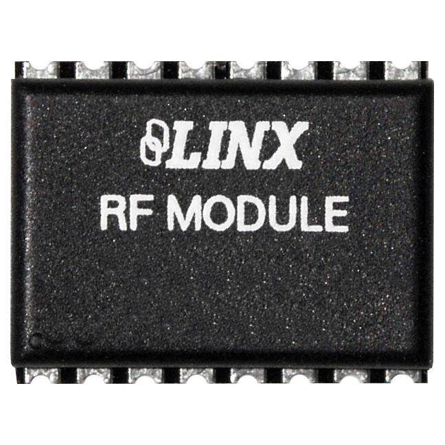
ICGOO电子元器件商城为您提供MICRF007YM由Micrel设计生产,在icgoo商城现货销售,并且可以通过原厂、代理商等渠道进行代购。 MICRF007YM价格参考¥20.54-¥20.54。MicrelMICRF007YM封装/规格:RF 接收器, QwikRadio® RF Receiver ASK,OOK 300MHz ~ 440MHz -96dBm 2.1kbps PCB,表面贴装 8-SOIC。您可以下载MICRF007YM参考资料、Datasheet数据手册功能说明书,资料中有MICRF007YM 详细功能的应用电路图电压和使用方法及教程。
| 参数 | 数值 |
| 产品目录 | |
| 描述 | IC RECEIVER UHF LOW POWER 8SOIC射频接收器 300-440MHz Receiver, 1.2kbps, 1.7mA With Shutdown( Lead Free) |
| 产品分类 | |
| 品牌 | Micrel |
| 产品手册 | |
| 产品图片 |
|
| rohs | 符合RoHS无铅 / 符合限制有害物质指令(RoHS)规范要求 |
| 产品系列 | RF集成电路,射频接收器,Micrel MICRF007YMQwikRadio® |
| 数据手册 | |
| 产品型号 | MICRF007YM |
| 产品目录页面 | |
| 产品种类 | 射频接收器 |
| 供应商器件封装 | 8-SOIC |
| 其它名称 | 576-1334 |
| 包装 | 管件 |
| 商标 | Micrel |
| 天线连接器 | PCB,表面贴装 |
| 存储容量 | - |
| 安装风格 | SMD/SMT |
| 封装 | Tube |
| 封装/外壳 | 8-SOIC(0.154",3.90mm 宽) |
| 封装/箱体 | SOIC-8 |
| 工作温度 | -40°C ~ 85°C |
| 工作电源电压 | 4.75 V to 5.5 V |
| 工作频率 | 300 MHz to 440 MHz |
| 工厂包装数量 | 95 |
| 带宽 | 0.43 MHz |
| 应用 | RKE |
| 数据接口 | PCB,表面贴装 |
| 数据速率(最大值) | 2.1 kbps |
| 最大工作温度 | + 85 C |
| 最小工作温度 | - 40 C |
| 标准包装 | 95 |
| 灵敏度 | -96dBm |
| 特性 | 自动调谐 |
| 电压-电源 | 4.75 V ~ 5.5 V |
| 电流-接收 | 3mA |
| 电源电压-最大 | 5.5 V |
| 电源电压-最小 | 4.75 V |
| 电源电流 | 2.4 mA |
| 类型 | Receiver/Data Demodulator |
| 系列 | MICRF007 |
| 调制或协议 | ASK,OOK |
| 频率 | 300MHz ~ 440MHz |


- 商务部:美国ITC正式对集成电路等产品启动337调查
- 曝三星4nm工艺存在良率问题 高通将骁龙8 Gen1或转产台积电
- 太阳诱电将投资9.5亿元在常州建新厂生产MLCC 预计2023年完工
- 英特尔发布欧洲新工厂建设计划 深化IDM 2.0 战略
- 台积电先进制程称霸业界 有大客户加持明年业绩稳了
- 达到5530亿美元!SIA预计今年全球半导体销售额将创下新高
- 英特尔拟将自动驾驶子公司Mobileye上市 估值或超500亿美元
- 三星加码芯片和SET,合并消费电子和移动部门,撤换高东真等 CEO
- 三星电子宣布重大人事变动 还合并消费电子和移动部门
- 海关总署:前11个月进口集成电路产品价值2.52万亿元 增长14.8%
_renders/CS4265-CNZR.jpg)

PDF Datasheet 数据手册内容提取
MICRF011 QwikRadiotm Receiver/Data Demodulator Preliminary Information General Description Features pi heclgn i sas,i100FRC IeM h ftnooisr edvecnah n ne,a101FRC IeMhT • Complete UHF receiver on a monolithic chip K F OrF)OeOdv-eiNyeO e,c(CKseInRo i rt soaesfcteiollmeperpriaw oidaRki wtQset asl’lerc igMniyolpme mt ees uciari t vgy.seo idlhoTnh cet • Frequency range 300 to 440 MHz ,ni -”at nucnoie-htatntia al“.doencoimved llA FR dna FI gninutsi ydlelhascii ltnpaimmhootcticuwaa eht ,CI hc ishewtanimlialuenam • Typical range over 200 meters with monopole yletelpmo cer asnoitcnu freviec e .Rstso cnoitcudor psecude rdn agninut antenna noitul otss owc oyllemert xte eeylbail eyrlhg i sahtilus e er. hdTetargetni eu r sat1i01FRC Ie Mhetsu a.c senBoitacilp psaseler iewmul ohvg irhof • ngise dgnizimini mly,ppa ot ysae ylemertxe si ti er,viecer oidar pihc-elgnis Data rates to 2.5kbps (SWP), 10kbps)DEXI F( .tekram ot emit gnivorpmi dna ,stsoc noitcudorp dna • Automatic tuning, no manual adjustment ehT 101FRCIM si a lanoitcn udfna n itpnel aevdiaurqgepu oteht • No Filters or Inductors required ,nodi nt ,dap ree mregvguewnonswoarin olrpdo,pmic1iv0o0rFpRCIM .edom DEXIF ni nehw troppus etar atad rehgih • Low Operating Supply Current— 2.4 mAzHM5 1t3a D,En X osIlieFat dtafonro meesmp eaood dwi1ntv01uo FfreRphCTIM • Fully pin compatible with MICRF001 dna WP.S n ID E,X eIsdF no eomeehlicktatiincvloneiu dtfanevnoc • eer,nvyi dehoctrei er w)trle o a hntlndraaareelcexplotiiulnfcs ist(oaa Very low RF re-radiation at the antenna htiw sA .kcolc ro latsyrc ecnerefer lanretxe na no desab ycneuqerf elgnis • er,viec eernydoretehrep ulsanoitnevn oycna eht transmitts uymcneuqe rf Direct CMOS logic interface to standard decoder e,yb dlyeelltllaaorrruetc nncheoatgciw a latsyrc ro WASecafruS( and microprocessor ICs or.tanoser )evaW citsuocA • Extremely low external part count rottaal l l)nialIcca soPns ,Wolr pe1S eede01eothFehmRntwtCisI(M ”sneda oyrlbe“ v.i etadtct n aeasarf di b fnhreeeaTeshhta ttabseertgar lanoit nte nvoent lorac ev o vihte i ut ufeaqdeloce ihaeewtv rhdFtnRab Applications sse lhti wetarep ona c101FRCI Meh tsuh T.sreviece revitareneger-repus • nev e,gninu tr ostnenopmo clanoitidd atuohti wsrettimsnar tC Levisnepxe Garage Door/Gate Openers .e n eey sdhdniotoIhmrtetehr e lpy lugsisoitls orpeovti ehecgheutroht • evisnep xses ehalt idwecalp e ernb alcatsy reccnerefer –cimar e%c5 .0 Security Systems or.tanoser • Remote Fan/Light Control ll Anoi t)creotteadl-utdsoomped (atad gniretlif si dedivorp no eht ru ofe .fony doneAngis eeoddbte esnretl ilfanret xoo,ens101FRCIM IMPORTANT: Items in bold type represent changes from yl l sayh nb tydredaeeh im ttter.rwecxssedbeehutnltlaed ibsifwdnaB the MICRF001 specification. Differences between the ot zHk52.1 ro )edom PWS( zHk5 ot zHk526.0 morf ,spets yranib ni egnar DEXI Fz(Hk01 etairporp pe ahmtargo rosptde eynl nroe s.e u)heTdom MICRF001 and -011 are identified in table 2, together with .tamrof noitaludom edoc dna etar atad no desab noitceles retlif design considerations for using the -011 in present MICRF001 designs. Typical Operating Circuit 385.5 MHz, 1200 bps OOK RECEIVER Micrel Inc. • 1 3 ,1ae5 C s9neoavJ SiernDut r9 o4F81 • USA • 0080-4 4) 98 l0 +e41t( • 0790-4 4)980 4x+1 (af • http://www.micrel.com
MICRF011 QwikRadio tm Micrel Ordering Information Part Number Temperature Range Package NB110FRCIM -40 (cid:176) C ot58+ (cid:176) C nPiIPD-41 MB110FRCIM -40 (cid:176) C ot58+ (cid:176) C niCPI-O4S1 Pin Configuration (DIP and SOIC) Pin Description Pin Number Pin Name Pin Function 1 SEL0 .ht drrioew ttdaln li ads uFBsepdimruoh a imT-nrysdei gleeDpoodllt raln.PnuiDrpDeVtni e eeSlbaT.1 3/2 VSSRF sihT nip si eht dnuorg nruter rof eht FR noitces fo eht .CI ehT ssapyb roticapa cdetcennoc morf FRDDVot VSSRF should have the shortest possible lead length. For best performance, connect VSSRF to VSSBB ta e h rtyelw po ypp,lu.ns e op.s eit B e (nhBgkm egSn oFruSinrRroV.wrfSur)ouSchhltVttfearp 4 ANT This is .d e ele vphyiu tl eot lc ccFa e,-eRnsrtcnriuanehpo ttnCnniiip o t. aeenvhniteetc neartupnI ecnadepmi si hgih TEF( )eta gy lhettiawmix oFrpp2pa fo .t)enccuinhtaitssicaarap pa(c srnooFitacilppa ne edw etk terycb oa eswmenstbnae opn,c -s edt dunnaelaexabmivnfo r ei tsvdnine eoetnhinaigbcimohal .noi tc eed etaySoo (trltdiprunvepaivnt oice ev eli lheeTats cnNneAo rii FdpteRnid SadioSdvtVaorp “Application Note 22, MICRF001 Theory of Operation”.) 5 FRDDV sihT nip si eht evitiso pylppus tupni rof eht FR noitces fo eht .CI BBDDV dna FRDDV dluohs ebdetcennoc directly at the IC pins. Connect a low ESL, low ESR decoupling capacitor from this pin to VSSRF, as short as possible. 6 VDDBB sihT nip si e hetvi tyilspopp utsupni rof e hdtn anboeistacbes fo eht .CI BBDDV dna FRD DdVluohseb connected directly at the IC pins. 7 HTC s s,ehtm m ccrr eoeia ooedh chhreftget )et wtueiatsCbmxlvcraiDoeaaaelh( rvwpvuTefaadhcotmed ecnerefe rrof eh tlanretn iatad g.nriotcailrsapmoc taerT siht sa a ssap-wol CR retlif htiw ecrecunosadepmi of 118kohms )zHM09. 4y=ctnfeu qCeSr OfrFoEfR( . Note that variation in source resistance with filter selection no longer exists, as it does for the MICRF001 . eeS( “Application Note 22, MICRF001 Theory of Operation”, section 6.4). A standard – 20% X7R ceramic capacitor is generally sufficient. 8 OD tuptuO atad .nip SOMC leve.lelbitapmoc 01/9 VSSBB sihT si eht dnuo rngruter rof eh tdna bneosiatbces fo eht .CI ehT ssapyb dna tsurdpoetttuicoceanpnaocc to VSSBB should have the shortest possible lead lengths. For best performance, connect VSSRF to BBSSV ta eht rewop ylppus ylno ,.e.i( peek BB SsSVtnerru cmorf gniw hoglfuorh tFRSSV nrute.r)htap 11 CGAC rgontiitca arrpg oaepfctinhIc-no receive AGC (Automatic Gain Control). The Decay/Attack time-constant (TC) ratio is nominally set as 10:1. Use of 0.47 m F rore tdaeed rynsge lirmgonmofo crtetssrebegnar performance. See “Application Note 22, MICRF001 Theory of Operation” for further information. 21 SEL1 .ht drrioew ttdaln li ads uFBsepdimruoh a imT-nrysdei gleeDpoodllt raln.PnuiDrpDeVtni e eeSlbaT.1 31 CSOFER sihT si eht gnimit ecnerefer rof pihc-no gninut dna .tnemngila tcennoC rehtie a cimarec rotanoser rolatsyrc n es)eit whnntte ie d,pbednBdneB oa pSrmeeSo(vdV ietr hudhtptni iwn .aptdkp uecVCplo5Anpl.iuc0oc Use ceramic resonators without integral capacitors. teoN tahtf i dteareop ni DXEIF e,dom a ltasyrct sum be; desu ervewho ni PWS ,eodme no yma esu rehitea latsyrc ro ceramic resonator. See “Application Note 22, MICRF001 Theory of Operation” rof sliatedno yc nneoiuqtecrefle sdna.ycarucca 41 SWEN This logic pin controls the operating mode of the MICRF011. When SWEN = HIGH, the MICRF011 is in SWP mode. This is the normal (default) mode of the device. When SWEN = LOW, the device operates e.erSe(vi eecneyrdoretehr enpouissrevnoc-el glnainsoit nsea vanoc “Application Note 22, MICRF001 Theory of Operation” r o)f.sliated sihT nip sy ilplua-ndreeltlnui pot.DDV December1 998b 2 110FRCIM
MICRF011 QwikRadio tm Micrel SEL0 SEL1 Demodulator Bandwidth (Hz) SWP Mode FIXED Mode 1 1 5000 10000 0 1 2500 5000 1 0 1250 2500 0 0 625 1250 Table 1 Nominal Demodulator (Baseband) Filter Bandwidth vs. SEL0, SEL1 and Mode No Design Change Retrofit Design Action . 1. Local Oscillator sweep range Reconsider Tx/Rx Frequency Alignment Error Budget, per App. Note 22. reduced 2X. Affects SWP mode If alignment tolerances cannot be met, consider: only. (1) tighten ceramic resonator tolerance, (2) replace ceramic resonator with crystal, or (3) not to upgrade to -011 2. Local Oscillator sweep rate reduced Impacts SWP mode maximum data rate. 2X. Affects SWP mode only. If data rate constraint cannot be met, consider (1) reduce system data rate by 2X, or (2) not to upgrade to -011 3. IF Center Frequency reduced 2X. Factor this change into Tx/Rx Frequency Alignment Error Budget. Affects both modes SWP and FIXED mode users of -001 must change crystal frequency. .DEXIF 4. IF Bandwidth reduced 2X. Affects Factor this change into Tx/Rx Frequency Alignment Error Budget. both modes SWP and FIXED. 5. FIXED mode Demod Filter cutoff For FIXED mode only, choose next lower filter frequency (via control pins frequencies increased 2X. Affects SEL0/1), to maintain same range performance FIXED mode only. 6. CTH Pin Impedance Recompute appropriate value of CTH capacitor, and change value on PCB 118k W @ ft=4.90 MHz [see Note 4]. Affects both modes SWP and .DEXIF Table 2 MICRF001/011 Change List and Design Retrofit Guidelines December1 998b 3 110FRCIM
MICRF011 QwikRadio tm Micrel ABSOLUTE MAXIMUM RATINGS Operating Ratings Supply Voltage (VDDRF, VDDBB) .................................+7V Supply Voltage (VDDRF, VDDBB) ..................4.75V to 5.5V Voltage on any I/O Pin .........................VSS-0.3 to VDD+0.3 Ambient Operating Temperature (T A )..........-40 (cid:176) C to +85 (cid:176) C Junction Temperature ..............................................+150 (cid:176) C Storage Temperature Range .....................-65 (cid:176) C to + 150 (cid:176) C Package Thermal Resistance q JA (14 Pin DIP) ........90 (cid:176) C/W Lead Temperature (soldering, 10 seconds) .............+ 260 (cid:176) C Package Thermal Resistance q JA (14 Pin SOIC)...120 (cid:176) C/W This device is ESD sensitive: Meets Class 1ESD test requirements (Human body Model, HBM), in accordance with MIL-STD-883C, Method 3015. Do not operate or store near strong electrostatic fields. Use appropriate ESD precautions. Electrical Characteristics Unless otherwise stated, these specifications apply for Ta=-40 (cid:176) C to 85 (cid:176) C, 4.75<VDD<5.5V. All voltages are with respect to Ground ; Positive currents flow into device pins. CAGC = 4.7µF, CTH = .047µF, VDDRF= VDDBB = VDD. REFOSC frequency =4.90MHz. Note: Items in bold represent changes from the MICRF001 specification. Parameter Test Conditions MIN TYP MAX UNITS Power Supply Operating Current 2.4 mA RF/IF Section Receiver Sensitivity Note 1, 3 -103 dBm IF Center Frequency Note 4 0.86 zHM IF 3dB Bandwidth Note 3, 4 0.43 zHM RF Input Range 300 440 zHM Receive Modulation Duty-Cycle 20 80 % Maximum Receiver Input Rsc = 50 W -20 dBm Spurious Reverse Isolation ANT pin, Rsc = 50 W Note 2 30 m Vrms AGC Attack / Decay ratio T(Attack) / T(Decay) 0.1 Local Oscillator Stabilization Time To 1% of Final Value 2.5 msec Demod Section CTH Source Impedance Note 5 118k W CTH Source Impedance Variation -15 +15 % Demod Filter Bandwidth SEL0 = SEL1 = SWEN = VDD, Note 4, 6 4160 zH Demod Filter Bandwidth SEL0 = SEL1 = VDD, SWEN = VSS 8320 zH Note 4, 6 Digital Section REFOSC Input Impedance 200k W Input Pullup Current SEL0, SEL1, SWEN = VSS 8 Aµ Input High Voltage SEL0, SEL1, SWEN 0.8VDD V Input Low Voltage SEL0, SEL1, SWEN 0.2VDD V Output Current DO pin, Push-Pull 10 Aµ Output High Voltage DO pin, Iout = -1µA 0.9VDD V Output Low Voltage DO pin, Iout = +1µA 0.1VDD V t,urpfTTtuO DO pin, Cload= 15pF 10 µsec Note 1: ytivitisneS si denifed sa eht egareva langis level derusaem ta eht tupni yrassecen ot eveihca 2-e01 tiB rorrE etaR .)REB( ehT tupni langis si denifed sa a orez-ot-nruter )ZR( mrofevaw htiw %05 egareva ytud elcyc ,.g.e( retsehcnaM dedocnE )ataD taa data rate of 300bps. The RF input is assumed to be matched into 50 W . Note 2: suoirupS esrever noitalosi stneserper eht suoirups stnenopmoc hcihw raeppa no eht FR tupni )TNA( nip derusaem otni05 W .hktr iogntwwnuat ipehnFnciRtam Note 3: ,ytivitisneS a ylnommoc deificeps revieceR ,retemarap sedivorp na noitacidni fo eht s’revieceR tupni derrefer ,esionyllareneg tupni lamreht .esion ,revewoH ti si elbissop rof a erom evitisnes reviecer ot tibihxe egnar ecnamrofrep on retteb naht taht foa ssel evitisnes ,reviecer fi eht ”rehte“ esion si ylbaicerppa rehgih naht eht lamreht .esion ”rehtE“ esion srefer ot rehtognirefretni “noise” sources, such as FM radio stations, pagers, etc. A retteb rotacidni fo reviecer egnar ecnamrofrep si yllausu nevig yb sti ,ytivitceleS netfo detats sa etaidemretnI ycneuqerF)FI( ro oidaR ycneuqerF )FR( ,htdiwdnab gnidneped no reviecer .ygolopot ytivitceleS si a erusaem fo eht noitcejer yb ehtreviecer fo ”rehte“ .esion eroM evitceles sreviecer lliw tsomla ylbairavni edivorp retteb .egnar ylnO nehw eht reviecer ytivitceles sios high that most of the noise on the receiver input is actually thermal will the receiver demonstrate sensitivity-limited performance. December1 998b 4 110FRCIM
MICRF011 QwikRadio tm Micrel Note 4: retemaraP selacs ylraenil htiw CSOFER ycneuqerf .tf roF yna CSOFER ycneuqerf rehto naht ,zHM09.4 etupmocwen retemarap eulav sa eht oitar CSOFER([ QERF ni( )zHM / ]09.4 * retemaraP[ eulaV @ .]zHM09.4 :elpmaxE roFCSOFER .q er eretuFt fle ]am,z VazH @rHM=a M0 P= 000 [r0.0ee.6.ut6.6le] (am z/ Va)H@r0Ma90P.9[4.*4 Note 5: retemaraP selacs ylesrevni htiw CSOFER ycneuqerf .tf roF yna CSOFER ycneuqerf rehto naht ,zHM09.4 etupmocwen retemarap eulav sa eht oitar 09.4[ / CSOFER( QERF ni( ])zHM * retemaraP[ eulaV @ .]zHM09.4 :elpmaxE roFCSOFER .q er eretuFt fle ]am,z VazH @rHM=a M0 P=000[0.9.6.64 ( / ) r0ee0ut..le ]6am*z VaH@rMa0P9[.4 Note 6: domeD retlif shtdiwdnab era detaler ni a yranib ,rennam os yna fo eht )rewol( lanimon retlif seulav yam eb devired ylpmisyb reeu tl g eaynsmvbiiad hri,tav2pi d,4 ro 8.d esraised Typical Performance Characteristics MICRF011 I vs Frequency DD (Temperature=25(cid:176)(cid:176) C, V =5.0V, SWP Mode) DD 6.10 5.60 5.10 I (mA) DD 4.60 4.10 3.60 3.10 2.60 2.10 1.60 250 275 300 325 350 375 400 425 450 475 500 Frequency (MHz) MICRF011 I vs Temperature DD (Frequency=315MHz, V =5.0V, SWP Mode) DD 3.30 3.10 2.90 2.70 I (mA) DD 2.50 2.30 2.10 1.90 -40 -20 0 20 40 60 85 Temperature (C) December1 998b 5 110FRCIM
MICRF011 QwikRadio tm Micrel MICRF011 Block Diagram 6 6 110FRCIM December1 998b
MICRF011 QwikRadio tm Micrel Functional Description transmitter is used for its mechanical stability), the user may choose to configure the MICRF011 as a standard Please refer to “MICRF011 Block Diagram”. Identified in the superheterodyne receiver (FIXED mode), mitigating the figure are the three principal functional blocks of the IC, aforementioned problem of a competing close-in signal. namely (1) UHF Downconverter, (2) OOK Demodulator, and This can be accomplished by tying SWEN to ground. Doing (3) Reference and Control. Also shown in the figure eraowt so forces the on-chip LO frequency to a fixed value. In capacitors (CTH, CAGC) and one timing component (CR), FIXED mode, the ceramic resonator would be replaced with usually a ceramic resonator. With the exception of a supply a crystal. Generally, however, the MICRF011 can be decoupling capacitor, these are all the external components operated in SWP mode, using a ceramic resonator, with needed with the MICRF011 to construct a complete UHF either LC or CRYSTAL/SAW based transmitters, without receiver. Three control inputs are shown in the block any significant range difference. diagram, SEL0, SEL1 and SWEN. Through these logic inputs the user can control the operating mode and The inputs SEL0 and SEL1 control the Demodulator filter programmable functions of the IC. These inputs are CMOS bandwidth in four binary steps (625Hz-5000Hz in SWP, compatible, and are pulled-up on the IC. 1250Hz-10000Hz in FIXED mode), and the user must select the bandwidth appropriate to his needs. Input SWEN selects the operating mode of the IC (FIXED mode or SWP mode). When low, the IC is in FIXED mode, Rolloff response of the IF Filter is 5 th order, while the and functions as a conventional superheterodyne receiver. demodulator data filter exhibits a 2 nd order response. When SWEN is high, the IC is in SWP mode. In this mode, Multiplication factor between the REFOSC frequency ft and while the topology is still superheterodyne, the local the internal Local Oscillator (LO) is 64.5X for FIXED mode, oscillator (LO) is deterministically swept over a range of and 64.25X for SWP mode (i.e., for ft = 6.00MHz in FIXED frequencies at rates greater than the data rate. When mode, LO frequency = 6.00MHz * 64.5 = 387MHz). coupled with a peak-detecting demodulator, this technique effectively increases the RF bandwidth of the MICRF011, so the device can operate in applications where significant Slicing Level and the CTH Capacitor Transmitter/Receiver frequency misalignment may exist. Extraction of the DC value of the demodulated signal for purposes of logic-level data slicing is accomplished by [Note: The swept LO technique does not affect the IF external capacitor CTH and the on-chip switched-cap bandwidth, so noise performance is not impacted relative to “resistor” RSC, indicated in the block diagram. The effective FIXED mode. In other words, the IF bandwidth is the same resistance of RSC is 118kohms. The value of capacitor (500kHz) whether the device is in FIXED or SWP mode.] CTH is easily calculated, once the slicing level time-constant is chosen. Values vary somewhat with decoder type, data Due to limitations imposed by the LO sweeping process, the pattern, and data rate, but typical Slicing Level time upper limit on data rate in SWP mode is approximately constants range 5-50msec. Optimization of the CTH value 2.5kbps. Data rates beyond 10kbps are possible in FIXED mode however. is required to maximize range, as discussed in “Application Note 22, MICRF001 Theory of Operation”, section 6.4. Examples of SWP mode operation include applications During quiet periods (i.e., no signal transmissions) the Data which utilize low-cost LC-based transmitters, whose transmit Output (DO pin) transitions randomly based on noise. This frequency may vary up to – 0.5% over initial tolerance, may present problems for some decoders. The most aging, and temperature. In this (patent-pending) mode, the common solution is to introduce a small offset (“Squelch”) LO frequency is varied in a prescribed fashion which results on the CTH pin so that noise does not trigger the internal in downconversion of all signals in a band approximately comparator. Usually 20-30mV is sufficient, and may be 1.5% around the transmit frequency. So the Transmitter introduced by connecting a several-Megohm resistor from may drift up to – 0.5% without the need to retune the the CTH pin to either VSS or VDD, depending on the desired Receiver, and without impacting system performance. Such offset polarity. Since the MICRF011 is an AGC’d receiver, performance is not achieved with currently available crystal- noise at the internal comparator input is always the same, based superheterodyne receivers, which can operate only set by the AGC. So the squelch offset requirement does not hAWtSiw or crystal based transmitters. change as the local “ether” noise changes from installation to installation. Note that introducing squelch will reduce [Note: In SWP mode only, a range penalty will occur in range modestly, so only introduce an amount sufficient to installations where there exists a competing signal of “quiet” the output. sufficient strength in this small frequency band of 1.5% around the transmit frequency. This results from the fact AGC Function and the CAGC Capacitor that sweeping the LO indiscriminately “sweeps” all signals within the sweep range down into the IF band. This same The signal path has automatic gain control (AGC) to penalty also exists with super-regenerative type receivers, increase input dynamic range. An external capacitor, as their RF bandwidth is also generally 1.5%. So any CAGC, must be connected to the CAGC pin of the device. application for a super-regenerative receiver is also an ehT ratio of decay-to-attack time-constant is fixed at 10:1 application for the MICRF011 in SWP mode.] (i.e., the attack time constant is 1/10th the decay time constant), and this ratio cannot be changed by the user. However, the attack time constant is selectable by the user For applications where the transmit frequency is accurately through the value of capacitor CAGC. set for other reasons (e.g., applications where a SAW 7 7 110FRCIM December1 998b
MICRF011 QwikRadio tm Micrel [By adding resistance from the CAGC pin to VDDBB or Here ft is in MHz. Connect a crystal of frequency ft to the VSSBB in parallel with the CAGC capacitor, the ratio of REFOSC pin of the MICRF011. 4 decimal-place accuracy decay-to-attack time-constant may be varied, although the on the frequency is generally adequate. The following table value of such adjustments must be studied on a per- identifies ft for some common Transmit frequencies when application basis. Generally the design value of 10:1 is the MICRF011 is operated in FIXED mode. adequate for the vast majority of applications.] See “Application Note 22”. Transmit Freq. )zHM (xtf )z H.tMqf( eCrSFOFER To maximize system range, it is important to keep the AGC 315 4.8970 control voltage ripple low, preferably under 10mVpp once 418 6.4983 the control voltage has attained its quiescent value. For this 433.92 6.7458 reason capacitor values ‡ 0.47uF are recommended. 2. Selecting REFOSC Frequency ft (SWP Mode) Reference Oscillator (REFOSC) and External Timing Element Selection of REFOSC frequency ft in SWP mode is much simpler than in FIXED mode, due to the LO sweeping All timing and tuning operations on the MICRF011 are process. Further, accuracy requirements of the frequency derived from the REFOSC function. This function is a reference component are significantly relaxed. single-pin Colpitts-type oscillator. The user may handle this pin in one of three possible ways: In SWP mode, ft is given by equation (3): (1) connect a ceramic resonator, or ft = ftx / 64.25. (3) (2) connect a crystal, or (3) drive this pin with an external timing signal. Connect a ceramic resonator of frequency ft to the REFOSC pin of the MICRF011. 2-decimal place accuracy is generally The third approach is attractive for further lowering system adequate. (A crystal may also be used if desired, but may cost if an accurate reference signal exists elsewhere in the be necessary to reduce the Rx frequency ambiguity if the Tx system (e.g., a reference clock from a crystal or ceramic frequency ambiguity is excessive. See Application Note 22 resonator-based microprocessor). An externally applied for further details.) signal should be AC-coupled, and resistively-divided down (or otherwise limited) to approximately 0.5Vpp. The specific 3. Selecting Capacitor CTH reference frequency required is related to the system transmit frequency, and the operating mode of the device as First step in the process is selection of a Data Slicing Level set by the SWEN control pin. See “Application Note 22, timeconstant. This selection is strongly dependent on MICRF001 Theory of Operation” for a discussion of system issues, like system decode response time and data frequency selection and accuracy requirements. code structure (e.g., existence of data preamble, etc.). This issue is too broad to discuss here, and the interested reader MICRF011 Frequency and Capacitor Selection should consult the Application Note 22. Selection of the REFOSC frequency ft, Slicing Level (CTH) Source impedance of the CTH pin is given by equation (4), capacitor, and AGC capacitor are briefly summarized in this ere htwf si ni:zHM section. Please see Application Note 22 for complete details. Rsc = 118k W * (4.90 / ft). (4) 1. Selecting REFOSC Frequency ft (FIXED Mode) Assuming that a Slicing Level Timeconstant TC has been established, capacitor CTH may be computed using As with any superheterodyne receiver, the difference equation (5): between the (internal) Local Oscillator (LO) frequency flo and the incoming Transmit frequency ftx must ideally equal /C T=HTC Rsc. (5) the IF Center frequency. Equation (1) may be used to compute the appropriate flo for a given :xtf flo = xtf – 1.064 * ( xtf /)093 (1) erehw xtf dna flo are in MHz. Note that two values of flo exist for any given ftx, distinguished as “high-side mixing” and “low-side mixing”, and there is generally no preference of one over the other. After choosing one of the two acceptable values of flo, use equation (2) to compute the REFOSC frequency ft: ft = flo / 64.5. (2) 8 8 110FRCIM December1 998b
MICRF011 QwikRadio tm Micrel 3. Selecting CAGC Capacitor capacitor CAGC. The attack current is nominally 15 m A, while the decay current is a 1/10th scaling of this, Selection of CAGC is dictated by minimizing the ripple on approximately 1.5 m A. Signal gain of the RF/IF strip inside the AGC control voltage, by using a sufficiently large the IC diminishes as the voltage on CAGC decreases. By capacitor. It is Micrel’s experience that CAGC should be in simply adding a capacitor to CAGC pin, the attack/decay the vicinity of 0.47 m F to 4.7 m F. Large capacitor values time constant ratio is fixed at 1:10. Further discussion on should be carefully considered, as this determines the time setting the attack time constant is found in “Application Note required for the AGC control voltage to settle from a 22, MICRF001 Theory of Operation”, section 6.5. completely discharged condition. AGC settling time from a Modification of the attack/decay ratio is possible by adding completely discharged (0-volt) state is given approximately resistance from CAGC pin either to VDDBB or VSSBB, as by equation (6): desired. D T = (1.333 * CAGC) – 0.44 (6) 4. DO Pin where CAGC is in microfarads, and D T is in seconds. The output stage for the Data Comparator (DO pin) is shown in Figure 4. The output is a 10µA push-10µA pull, switched I/O Pin Interface Circuitry current stage. Such an output stage is capable of driving CMOS-type loads. An external buffer-driver is Interface circuitry for the various I/O pins of the MICRF011 is recommended for driving high capacitance loads. shown in Figures 1 through 6. Specific information regarding each of these circuits is discussed in the following 5. REFOSC Pin sub-paragraphs. Not shown are ESD protection diodes which are applied to all input and output pins. ehT REFOSC input circuit is shown in Figure 5. Input impedance is quite high (200k W ). This is a Colpitts 1. ANT Pin oscillator, with internal 30pF capacitors. This input is intended to work with standard ceramic resonators, The ANT pin is internally AC-coupled via a 3pF capacitor, to connected from this pin to VSSBB, although a crystal may be used instead, where greater frequency accuracy is required. The resonators should not contain integral capacitors, since these capacitors are contained inside the IC. Externally applied signals should be AC-coupled, amplitude limited to approximately 0.5Vpp. The nominal DC bias voltage on this pin is 1.4V. 6. Control Inputs (SEL0, SEL1, SWEN) Control input circuitry is shown in Figure 6. The standard input is a logic inverter constructed with minimum geometry MOSFETs (Q2, Q3). P-channel MOSFET Q1 is a large channel length device which functions essentially as a “weak” pullup to VDDBB. Typical pullup current is 5 m A, Figure 1 ANT Pin leading to an impedance to the VDDBB supply of typically an RF N-channel MOSFET, as shown in Figure 1. M1 W . Impedance on this pin to VSS is quite high at low frequencies, and decreases as frequency increases. In the UHF frequency range, the device input can be modeled as 6.3k W in parallel with 2pF (pin capacitance) shunt to VSSRF. 2. CTH Pin Figure 2 illustrates the CTH pin interface circuit. CTH pin is driven from a P-channel MOSFET source-follower biased with approximately 10µA of bias current. Transmission gates TG1 and TG2 isolate the 6.9pF capacitor. Internal control signals PHI1/PHI2 are related in a manner such that the impedance across the transmission gates looks like a “resistance” of approximately 118k W . The DC potential on the CTH pin is approximately 1.6V. 3. CAGC Pin Figure 3 illustrates the CAGC pin interface circuit. The AGC control voltage is developed as an integrated current into a 9 9 110FRCIM December1 998b
MICRF011 QwikRadio tm Micrel Figure 3 CAGC Pin Figure 2 CTH Pin Figure 6 SEL0, SEL1, SWEN Figure 4 DO Pin Figure 5 REFOSC Pin 10 10 110FRCIM December1 998b
MICRF011 QwikRadio tm Micrel Typical Application The Figure below illustrates a typical application for the MICRF011 UHF Receiver IC. Operation in this example is at 385.5MHz, and may be customized by selection of the appropriate reference frequency (CR1), and adjustment of the antenna length. The value of C4 would also change, if the optional input filter is used. Changes from the 1kbps data rate may require a change in the value of R1. The Bill of Materials is shown in the accompanying chart. noita c1i1 l0lpFapRcACiIpMyT ycneuqe rgFnitare pz OH5M.583 noi tsaprbekp1O tiB-6 sserddAedoceD Bill of Materials Item Part Number Manufacturer Description U1 110FRCIM Micrel UHF Receiver U2 D21-TH Holtek Logic decoder CR1 GM00.6ASC ataruM 6.00MHz Cer. Res. D1 SSF-LX100LID xemuL DEDREL R1 Bourns 68k, 1/4W ,5% R2 Bourns 1k,1/4W, 5% C1 Panasonic 4.7µF, Dip Tant. Cap C3 Panasonic 0.47µF, Dip Tant. Cap C2 Panasonic 2.2µF, Dip Tant. Cap C4 Panasonic 8.2pF, COG Cer. Cap Vendor Telephone Fax Bourns (909) 781-5500 (909) 781-5273 Holtek (408) 894-9046 (408) 894-0838 xemuL (800) 278-5666 (847) 359-8904 ataruM (800) 241-6574 (770) 436-3030 Panasonic (201) 348-7000 (201) 348-8164 MICREL INC. 1849 FORTUNE DRIVE SAN JOSE, CA 95131 USA TEL -4 4)98 0 4+1( 0 080 XAF 0 790-4 4)98 0 4+1( WEB http://www.micrel.com no istiahm T rsdoiefvneiil eobt eebtar u ,c de crnlyaeabtvaieilwlio ebh orisn sidneompussesr ayb lerci Mrof sti esu ron ro ftne myenga nfi orsftnnieta pro rehsttohgir fo driht seitrap gnitluser morf sti .esu oN esnecil si detnarg yb noitacilpmi ro esiwrehto rednu yna tnetap ro tnetap thgir fo lerciM .cnI This is preliminary information and a final specification has not been completed. Before making any final design determination, consult with Micrel for final specifications. detaropro clneIr c8i9M91© December1 998b 11 110FRCIM
Mouser Electronics Authorized Distributor Click to View Pricing, Inventory, Delivery & Lifecycle Information: M icrochip: MICRF007YM TR MICRF007YM MICRF011YM MICRF011YM TR MICRF011YN MICRF007YM-TR MICRF011YM-TR